
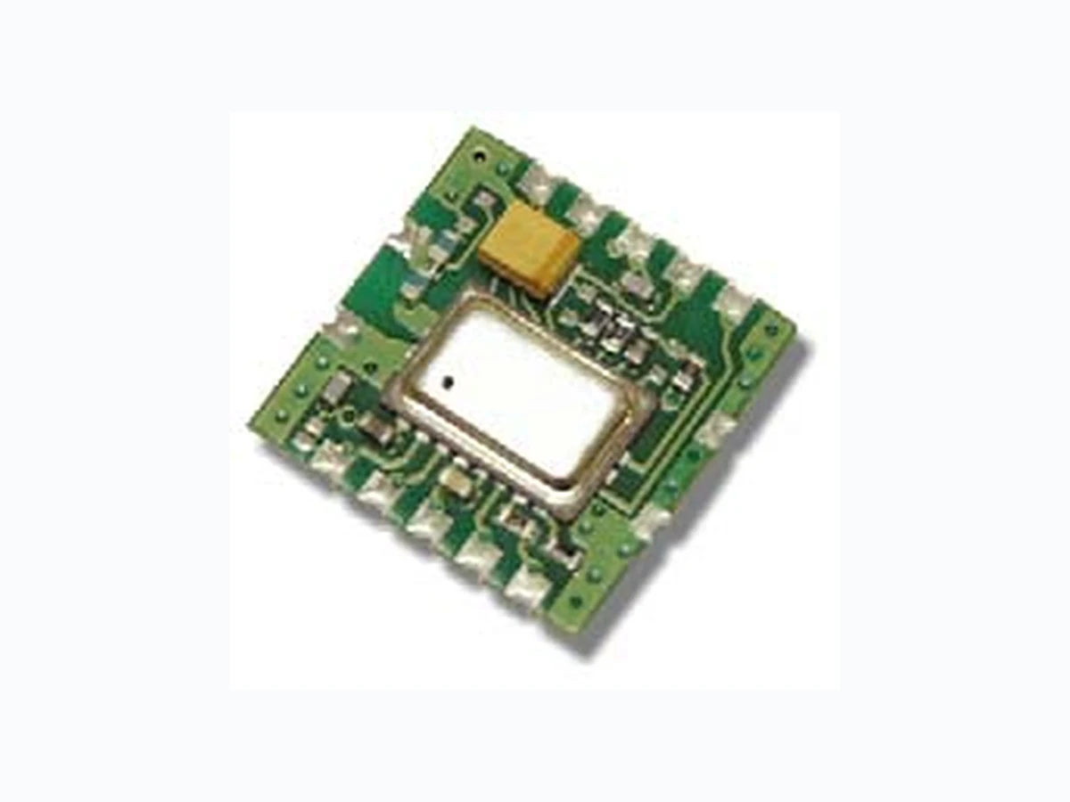
DR4001 MURATA
Document overview
- Manufacturer or author: Provided By www.digicamel.com(FREE DATASHEET DOWNLOAD SITE)
- PDF pages: 2
Technical content
www.RFM.com E-mail: info@rfm.com Page 1 of 2 ©2008 by RF Monolithics, Inc. DR4001 - 4/8/08 Characteristic Sym Notes Minimum Typical Maximum Units Operating Frequency fO 868.15 868.55 MHz Data Rate OOK 19.2 kbps ASK 115.2 Transmitter Performance (OOK @ 2.4 kbps) Peak Input Current, 3 Vdc Supply ITP 12 mA Peak Output Power PO 0.75 mW Turn On/Turn Off Time tON/tOFF 12/6 µs Power Supply Voltage Range VCC 2.7 3.5 Vdc Operating Ambient Temperature T A -20 +65 °C
- Designed for Short-Range Wireless Data Communications Supports up to 115.2 kbps Encoded Data Transmissions 3 V, Low Current Operation plus Sleep Mode Ready to Use OEM Module The DR4001 transmitter module is ideal for short-r ange wireless data applications where robust operation, small size and low power consumption are required. The DR4001 utilizes RFM’s TX6001 amplifier-sequenced hybrid (ASH) architecture to achieve this unique blend of characteristics. The transmitter includes provisions for on-off keyed (OOK) and ASK modulation. The transmitter employs SAW filtering to suppress output harmonics, facilitating compliance with ETSI 300 220 and similar regulations. The DR4001 includes the TX6001 plus all configuration components in a ready-to-use PCB assembly, excellent for prototyping and intermediate volume production runs. Absolute Maximum Ratings Rating Value Units Power Supply and All Input/Output Pins -0.3 to +4.0 V Non-Operating Case Temperature -50 to +100 °C Soldering Temperature (10 seconds) 230 °C
868.35 MHz
.70 .25 .20 .165 .70 .10 DR4000 Outline Drawing Dimensions in inches DR4001 Outline Drawing
www.RFM.com E-mail: info@rfm.com Page 2 of 2 ©2008 by RF Monolithics, Inc. DR4001 - 4/8/08 Pin Desciptions Pin Name Description 1V C C 5T X I N The TX IN pin is connected to the transmitter TXMOD pin throu gh a 4.7 K resistor on the circuit board. Additional series resis- tance will often be required between the modulation source and the TX IN pin, depending on the desired output power and peak modulation voltage (3.3 K typical for a peak modulation voltage of 3 volts). Saturated output power requires about 450 µA of drive current. Peak output power P O for a 3 Vdc supply is approximately: PO = 4.8*((VTXH - 0.9)/(RM + 4.7))2, where PO is in mW, peak modulation voltage VTXH is in volts and external modulation resis- tor RM is in kilohms This pin must be held low in the receive and sleep modes. Please refer to section 2.9 of the ASH Transceiver Designer's Guide for additional information. 6, 7 GND 8N C 9V C C This is the positive supply voltage pin for the module. The operati ng voltage range is 2.7 to 3.5 Vdc. It is also possible to u se Pin 1 as the Vcc input. Please refer to the Pin 1 description above. 10 GND This is the supply voltage return pin.
11 CTR1
CTR1 and CTR0 select the transmit modes. CTR1 high and CTR0 low place the unit in the ASK transmit mode. CTR1 low and CTR0 high place the unit in the OOK transmit mode. CTR1 and CTR0 both low place the unit in the power down (sleep) mode. CTR1 is a high-impedance input (CMOS compatible). An input voltage of 0 to 200 mV is interpreted as a logic low. An input voltage of Vcc - 200 mV or greater is interpreted as a logi c high. An input voltage greater than Vcc + 200 mV should not be applied to this pin. This pin must be held at a logic level; it cannot be left unconnected.
12 CTR0
(T/S) “T” =1 for transmission, “S” =0 for sleep mode 13 RFIO RFIO is the RF output pin. A matching circuit for a 50 ohm l oad (antenna) is implemented on the circuit board between this pin and the transceiver SAW filter transducer. 14 RF GND This pin is the RF ground (return) to be used in conjunction with the RFIO pin. For example, when connecting the module to an external antenna, the coaxial cable ground is connected this pin and the coaxial cable center conductor is connected to RFIO. Dat a I n
3 Vdc
3.3k DR4001 Application OOK Circuit Data In Appl i cat i on ASK Ci rcui t DR4000 T/S 12345 89101112 3.3k Application ASK Circuit DR4001