
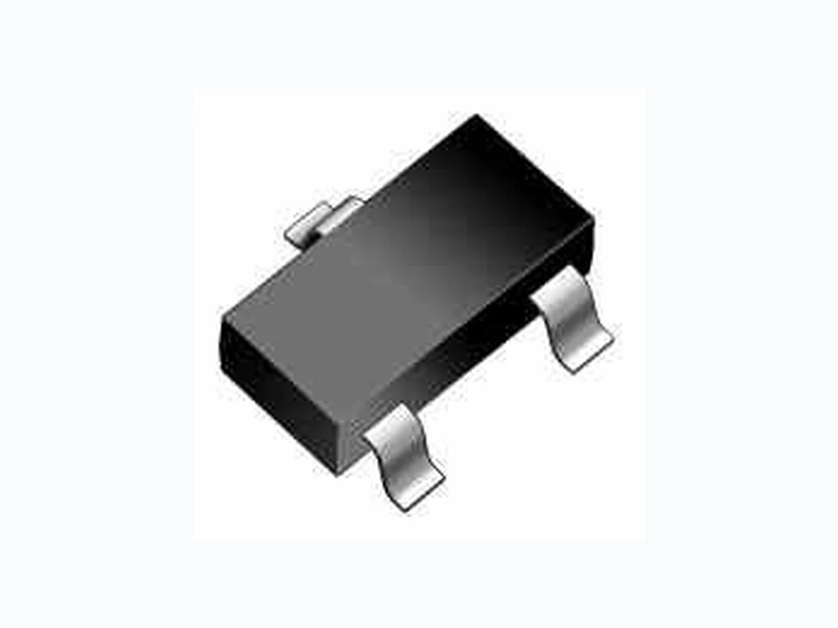
DMG3130LQ LEIDITECH
Document overview
- Manufacturer or author: Provided By www.digicamel.com(FREE DATASHEET DOWNLOAD SITE)
- PDF pages: 6
Technical content
Features
ID (at VGS=-10V) -5.0A RDS(ON) (atVGS=-10V) 50mΩ(Max) RDS(ON) (atVGS=-4.5V) 65mΩ(Max) RDS(ON) (atVGS=-2.5V) 90mΩ(Max) AbsoluteMaximumRatings T A=25°C unlessotherwisenoted Parameter Symbol Maximum Units Drain-SourceVoltage VDS -30 V Gate-SourceVoltage VGS ±12 V DrainCurrent-Continuous TC=25°C ID -5.0 A TC=100°C ID -3.5 A DrainCurrent – Pulsed IDM -20 A MaximumPower Dissipation PD 2.1 W JunctionandStorage TemperatureRange TJ,TSTG -55To 150 ℃ Thermal Characteristics Parameter Symbol Typ Max Unit ThermalResistancejunction-case RθJc 1.1 ℃ /W ThermalResistanceunction-to-Ambient RθJA 60 ℃ /W G D S G D S SOT23 Enhancement Mode Power MOSFET P-Channel Rev : www.leiditech.com 01.06.2018 1/6 DMG3130LQ DMG3130LQ
ElectricalCharacteristics(TJ=25 ℃ unlessotherwisenoted) Symbol Parameter Condition Min Typ Max Unit STATIC PARAMETERS BVDSS Drain-SourceBreakdown Voltage VGS=0VID=-250μA -30 V IDSS ZeroGate VoltageDrainCurrent VDS=-30V,VGS=0V 1 μA IGSS Gate-BodyLeakageCurrent VGS=±12V,VDS=0V ±100 nA VGS(th) Gate ThresholdVoltage VDS=VGS,ID=-250μA -0.5 -0.9 -1.5 V RDS(ON) Drain-Source On-State Resistance VGS=-10V, ID=-4.0A 41 50 mΩ VGS=-4.5V, ID=-3.5A 50 mΩ VGS=-2.5V, ID=-2.0A 60 90 mΩ DYNAMICPARAMETERS Clss Input Capacitance VDS=-15V,VGS=0V, F=1.0MHz 640 pF Coss OutputCapacitance 80 pF Crss ReverseTransferCapacitance 55 pF SWITCHINGPARAMETERS td(on) Turn-onDelayTime VDS=-15V,ID=-1A, VGS=-10V, RG=3Ω 6.5 nS tr Turn-onRiseTime 3.5 nS td(off) Turn-Off DelayTime 41 nS tf Turn-Off FallTime 9 nS Qg Total GateCharge VDS=-15V,ID=-4.0A, VGS=-10V 14 nC Qgs Gate-SourceCharge 1.5 nC Qgd Gate-DrainCharge 1.6 nC VSD DiodeForward Voltage VGS=0V,ISD=-1A 0.72 1.4 V Rg Gateresistance VGS=0V,V DS=0V, F=1MHz 7 Ω Note: 1. RepetitiveRating:Pulsedwidth limitedbymaximumjunctiontemperature. 2. Thedata testedbypulsed,pulsewidth ≦ 300us,dutycycle ≦ 2%. 3. Essentiallyindependentof operatingtemperature. Rev : www.leiditech.com 01.06.2018 2/6 DMG3130LQ
TYPICAL ELECTRICAL AND THERMAL CHARACTERISTICS 2 2 4 4 6 6 8 8 1 10 0 0 0 5 5 1 10 0 1 15 5 --VVG GS S(Vo (Vol lts ts) ) Q Qgg (n (nC C) ) F Fi ig gu ur re e 7 7: : G Ga ate te-C -Ch ha ar rg ge e C Ch ha ar ra ac cte ter ri is sti tic cs s 0 0 2 20 00 0 4 40 00 0 6 60 00 0 8 80 00 0 1 10 00 00 0 00 55 1100 1155 2200 2255 C Ca ap pa ac ci ita tan nc ce e (p (pF F) ) -V -VDDS S(Vo (Vol lts ts) ) F Fi ig gu ur re e 8 8: : C Ca ap pa ac ci ita tan nc ce e C Ch ha ar ra ac cte ter ri is sti tic cs s C Ci iss ss C Co oss ss C Cr rss ss V VD DS S= =-1 -15 5V V I ID D= =-4 -4A A 1 1 1 10 0 1 10 00 0 1 10 00 00 0 1 10 00 00 00 0 Po Pow we er r (W (W) ) Pu Pul ls se e W Wi id dth th (s (s) ) F Fi ig gu ur re e 1 10 0: : Si Sin ng gl le e Pu Pul ls se e Po Pow we er r R Ra ati tin ng g J Ju un nc cti tio on n-to -to- - A Am mb bi ie en nt t (N (No ote te F F) ) T TA A= =2 25 5° °C C 0 0. .0 0 0 0. .1 1 1 1. .0 0 1 10 0. .0 0 1 10 00 0. .0 0 0 0. .0 01 1 0 0. .1 1 1 1 1 10 0 1 10 00 0 --I ID D( (A Am mp ps s) ) - -V VD DS S( (V Vo ol lt ts s) ) F Fi ig gu ur re e 9 9: : M Ma ax xi im mu um m F Fo or rw wa ar rd d B Bi ia as se ed d S Sa af fe e O Op pe er ra at ti in ng g A Ar re ea a ( (N No ot te e F F) ) 1 10 0µ µs s 1 10 0s s 11mm ss D DC C RR DD S(OS(ONN )) lliimm iitteedd T TJ J(M (Ma ax x) )= =1 15 50 0° °C C T TA A= =2 25 5° °C C 1 10 00 0µ µs s 1 10 0m ms s 0.001 0.01 0.1 ZθθθθJA Normalized Transient Thermal Resistance Pulse Width (s) Figure 11: Normalized Maximum Transient Thermal Impedance (Note F) Single Pulse D=T on/T TJ,PK=TA+PDM .ZθJA.RθJA Ton T PD In descending order R θJA=125°C/W Rev : www.leiditech.com 01.06.2018 4/6 DMG3130LQ
G Ga at te e C Ch ha ar rg ge e T Te es st t C Ci ir rc cu ui it t & & W Wa av ve ef fo or rm m - - ++ - - + + - -1 10 0V V V Vd dd d V Vg gs s I Id d Vgs Rg DUT VD C V Vg gs s V Vd ds s Id Vgs U Un nc cl la am mp pe ed d I In nd du uc ct ti iv ve e S Sw wi it tc ch hi in ng g ( (U UI IS S) ) T Te es st t C Ci ir rc cu ui it t & & W Wa av ve ef fo or rm ms s V Vd ds s L L - - 2 2 EE A A R R = = 1 1/ /2 2 L LI IA AR R B BV VD DS SS S IAR Ig V gs VD C DU T L Vg s Isd Diode Recovery Test Circuit & Waveforms Vd s - Vd s + dI/dt RM rr Vd dVdd Q = - Idt t rr -Isd -Vds F V VD DC C D DU UT T V Vd dd d V Vg gs s V Vd ds s V Vg gs s R RL L R Rg g R Re es si is st ti iv ve e S Sw wi it tc ch hi in ng g T Te es st t C Ci ir rc cu ui it t & & W Wa av ve ef fo or rm ms s - - V Vg gs s V Vd ds s t t t t t t t t t t t t 9 90 0% % 1 10 0% % r r d d( (o of ff f) )f f o of ff f d d( (o on n) ) Rev : www.leiditech.com 01.06.2018 5/6 DMG3130LQ
Symbol Dimensions In Millimeters Dimensions In Inches Max Min Max Min A 1.150 0.900 0.045 0.035 A1 0.100 0.000 0.004 0.000 A2 1.050 0.900 0.041 0.035 b 0.500 0.300 0.020 0.012 c 0.150 0.080 0.006 0.003 D 3.000 2.800 0.118 0.110 E 1.400 1.200 0.055 0.047 E1 2.550 2.250 0.100 0.089 e 0.95 TYP. 0.037 TYP. e1 2.000 1.800 0.079 0.071 L 0.55 REF. 0.022 REF. L1 0.500 0.300 0.020 0.012 L2 0.25 TYP. 0.01 TYP. θ 8° 0° 8° 0° SOT23 PACKAGE INFORMATION Shanghai Leiditech Electronic Co.,Ltd Email: sale1@leiditech.com Tel : +86- 021 50828806 Fax : +86- 021 50477059 Rev : www.leiditech.com 01.06.2018 6/6 DMG3130LQ