

 Download PDF
DF64 HIROSE
Document overview
- PDF pages: 6
Technical content
Page 1
(UL pending)
Y
X
±0.5mm
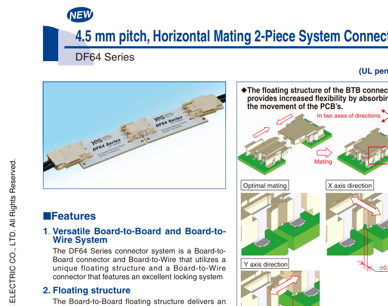
increased connection range together with a wide effective mating length and width. The unique stress-free contact structure was designed to
MAX 2mm
absorb movement and misalignment between serial
Figure 1
PCBs and ensure a continuous connection. (Please refer to Figure 1)
Movement tolerance range for the X axis: ±0.5 mm Movement tolerance range for the Y axis: MAX 2 mm
3. Reliable contact design
(B-to-B connection)
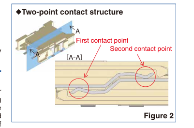
Our two-point contact structure provides a highly reliable contact system. (Please refer to Figure 2)
4. Stress free side-locking system for
Board-to-Wire connections
The BTW side-locking structure provides a clear tactile click to confirm completion of the mating process and also allows for a visual check on the side locks. The structure endures wiring stress and prevents the wires from being pulled out of
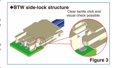
alignment. (Please refer to Figure 3)
5. 350V voltage capacity
Its unique mating structure secures a creepage distance of no less than 3.2 mm between the contacts and produces a 350 V voltage capacity.
6. PCB layout simplification
The DF64 connector system shares one common receptacle. This helps to simplify the PCB layout by accepting the BTB header and the BTW cable plug.
7. Resistant to high heat
These connectors can operate in temperatures of up to 105ç
2013.11
Page 2
■Product Specifi cations
| Ratings | Current Rating (Note 1) | BtoB | BtoW | Operating Temperature Range: -55 ~ to 105℃ (Note 2) Operating Humidity Range : 20 to 80% (Note 3) | ||
| 5A | AWG#18 | AWG#20 | AWG#22 | |||
| 5A | 4A | 3A | ||||
| Voltage Rating | AC/DC 350V | Storage Temperature Range: -10 to 60℃ (Note 4) Storage Humidity Range : 40 - 70% (Note 4) | ||||
| Item | Specifications | Conditions |
|---|---|---|
| 1. Insulation resistance | No less than 1,000 Mø | Measured at DC 500 V |
| 2. Withstand voltage | No fl ashover or breakdown | AC 1, 500 V is applied for one minute. |
| 3. Contact resistance | 30 Mø max | Measured at no more than DC 6 V, 100 mA (DC or 1,000 Hz) |
| 4. Vibration Resistance | No electrical discontinuity of 1µs or greater | Frequency 10-55 Hz, half amplitude 0.75 mm, 10 cycles in each of three directions(axes) |
| 5. Shock Resistance | No electrical discontinuity outage of 1µs or greater | Accelerated velocity: 490 m/s2, for 11 ms, half-sine in 3 directions, 3 times for each of the three directions (axes) |
| 6. Moisture- resistance | ■ Contact resistance 30 Mø max ■ Insulation resistance 1,000 Mø minimum | Temperature: 40 ±2ç; humidity: 90 to 95%, left as it is for 96 hours |
| 7. Temperature cycles | ■Contact resistance 30 Mø max ■Insulation resistance 1,000 Mø minimum | -55ç for 30 minutes → 5 to 35ç for 2 to 3 minutes →105ç for 30 minutes → 5 to 35ç for 2 to 3 minutes) in 5 cycles |
| 8. Durability | ■Contact resistance 30 Mø max | ■Number of matings/unmatings 10 mating cycles |
| 9. Resistance to solder heat | The resin components will not become deformed or loose performance due to deformities | Refl ow: according to the Recommended Temperature Profi le Hand soldering: temperature of soldering iron at 350ç±10ç for 3 seconds |
(Note 1) This is the maximum current rating while all pins are powered or used as all power lines. (Note 2) Includes the temperature rise of power lines. (Note 3) Use without condensation on parts. (Note 4) The storage condition refers to long-term storage of the product on the shelf before assembly. Please use the operating temperature for temporary storage such as pre-assembly and during shipping.
■Materials
| Product | Part | Materials | Finish | UL spec. |
|---|---|---|---|---|
| Receptacle | Insulator | LCP | Beige | UL94V-0 |
| Contact | Copper alloy | Tin-plating | − | |
| Reinforcing metal fi ttings | Brass | Tin-plating | − | |
| Header | Insulator | LCP | Beige | UL94V-0 |
| Contact | Copper alloy | Tin-plating | − | |
| Reinforcing metal fi ttings | Brass | Tin-plating | − | |
| Crimp case | Insulator | LCP | Beige | UL94V-0 |
| Crimp contact | Contact | Phosphorous Bronze | Tin-plating | − |
■Product Number Structure
Refer to the charts below for determining specifi c part number characteristics. Please select connectors listed in this catalog when placing orders and be sure to check the latest delivery specifi cations at the time of ordering the product.
- Connector
DF 64 - \* S - 4.5 H
❶ ❷ ❸ ❹
❺ ❻
DF 64 - \* P - 4.5 H
| ❶Series Name: DF | ❺Pitch : 4.5 mm |
| ❷Series No.: 64 | ❻Wiring type H: SMT Right Angle Type C: crimp housing |
| ❸Number of contacts: 2, 3 | |
| ❹Connector type S: receptacle P: plug |
❶ ❷ ❸ ❹
❺ ❻
DF 64 - \* P - 4.5 C
❶ ❷ ❸ ❹
❺ ❻
- Contact
DF 64 - 1822 PCF
❶ Applicable wire size
❷ Packaging style PCF: In-line plug plug contact, on reel
1822 : 18 – 22 AWG
❶ ❷
PC: In-line plug contact, loose piece
Page 3
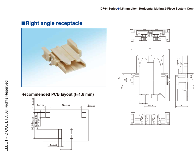
P=4.5±0.05
| Part Number. | HRS No. | No. of Contacts | A |
|---|---|---|---|
| DF64-2S-4.5H | 667-1002-9-00 | 2 | 14.4 |
| DF64-3S-4.5H | Under development | 3 | 18.9 |
B 11.8 16.3
(Note) This product is sold 500 connectors per reel. Please order by full reel quantities.
- Tape and Reel dimensions
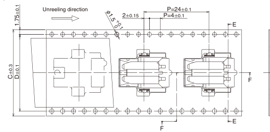
E-E
F-F
| Part Number | HRS No. | No. of Contacts | C |
|---|---|---|---|
| DF64-2S-4.5H | 667-1002-9-00 | 2 | 32 |
| DF64-3S-4.5H | Under development | 3 | 44 |
D 28.4 40.4
Page 4
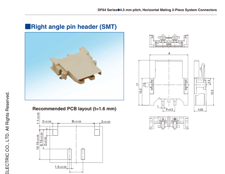
| Product No. | HRS No. | No. of Contacts A |
| DF64-2P-4.5H | 667-1001-6-00 | 2 14.4 |
| DF64-3P-4.5H | Under development | 3 18.9 |
B 11.8 16.3
(Note) This product is sold 500 connectors per reel. Please order by full reel quantities.
- Tape and Reel dimensions
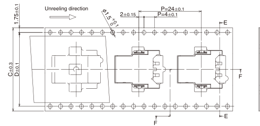
E-E
F-F
| Product No. | HRS No. | No. of Contacts C |
| DF64-2P-4.5H | 667-1001-6-00 | 2 32 |
| DF64-3P-4.5H | Under development | 3 44 |
D 28.4 40.4
Page 5
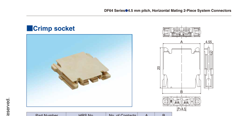
| Part Number | HRS No. | No. of Contacts | A |
|---|---|---|---|
| DF64-2P-4.5C | 667-1003-1-00 | 2 | 18.4 |
| DF64-3P-4.5C | Under development | 3 | 22.9 |
B [Specifi cation Number] 19.0 None: 1 package contains 23.5
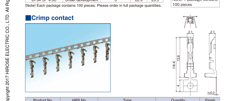
| Product No. | HRS No. | Type Quan | tity Finish |
|---|---|---|---|
| DF64-1822PCF | 667-1004-4-00 | Reel contact (Note 1) 1 reel = 5,0 | 00 pieces Tin-plating 100 pieces |
| DF64-1822PC | Under development | Loose piece contact (Note 2) 1 package = |
(Note 1) This product is sold 5,000 pieces per reel. Please order by full reel quantities. (Note 2) Each package contains 100 pieces. Please order in full package quantities.
- Applicable wire (Tinned, annealed copper wire)
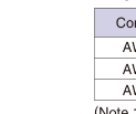
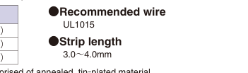
| Conductor size (Core structure) | Jacket Diameter |
| AWG (34 pieces/Ø 0.18 mm) | UL1015(Ø2.9mm) |
| AWG (21 pieces/Ø 0.18 mm) | UL1015(Ø2.6mm) |
| AWG (17 pieces/Ø 0.16 mm) | UL1015(Ø2.4mm) |
(Note 1) Applicable wires will have conductors that are comprised of annealed, tin-plated material. (Note 2) Please contact your local Hirose sales rep if you plan on using wires other than those listed above.
□Applicable crimping tool
| Item | Part Number | HRS No. | Applicable co |
|---|---|---|---|
| Applicator | AP105-DF64-1822 | CL901-4633-9-00 | DF64-1822P |
| Press body | CM-105 | CL901-0005-4-00 | − |
| Hand tool | HT801/DF64-1822 | Under development | DF64-1822 |
| Extraction tool | DF62/RE-MD | CL902-4645-4-00 | DF64-1822P DF64-1822 |
(Note 1) Please conduct crimping work according to the "Crimping work standards" and "Crimping condition table". (Note 2) Hirose does not cover damage created by the use of unapproved Hirose Tools. Please contact your local Hirose Sales for clarifi cation. (Note 3) Hand tools do not have replaceable dies. (Note 4) Approved wire is limited to UL1015; 18, 20, 22 AWG.
Page 6
□ Precautionary notes
| 1. Recommended Temperature Profi le (Compatible with lead-free soldering) | [Applicable Conditions] 1. Peak temperature 2. Heating unit: no less than 220℃ for no more than 60 seconds 3. Preheating unit: 150 to 180℃ for 90 to 120 seconds 4. Number of times: 2 times max. * Measurement is conducted at the contact lead part Please check the mounting conditions before use. Conditions such as solder paste types, manufacturer, PCB size and any other soldering materials may alter the performance of such materials. (Note 1) T his temperature profi le is a recommended value only; please contact your Hirose Sales Rep for more information |
|---|---|
| 2. Recommended hand soldering conditions | Temperature of soldering iron: 350±10ç, soldering time: no more than 3 seconds |
| 3. Recommended screen thickness, aperture ratio (pattern surface ratio) | Thickness: 0.1 mm, aperture ratio: 100% |
| 4. Warping of the Board | A maximum of 0.02 mm at the center of connector, as measured from either end of the connector |
| 5. Cleaning Conditions | IPA cleaning is allowed. (Cleaning is not recommended because cleaning may change the push/pull feeling etc. Please contact your local Hirose representative prior to the use of any cleaning agents. ) |
| 6. Important Notes | ■ When inserting the crimp contact into the crimp socket, do not insert it at a slanted angle to maintain the reliability of its performance. ■ Please use caution when mating/unmating this connector if it has not been mounted onto the PCB, doing so could deform or damage the contacts. ■ Do not pull on the wires of this connector as this may cause damage to the connector. ■ During the hand soldering process, make sure to not apply too much fl ux. Doing so may cause a solder wicking problem. ■ This product may experience some differences in color from one production lot to another. This color difference does not infl uence the performance of the connector. |

6-3,Nakagawa Chuoh-2-Chome,Tsuzuki-Ku,Yokohama-Shi 224-8540,JAPAN TEL: +81-45-620-3526 Fax: +81-45-591-3726 http://www.hirose.com http://www.hirose-connectors.com
The characteristics and the specifications contained herein are for reference purpose. Please refer to the latest customer drawings prior to use. The contents of this catalog are current as of date of 11/2013. Contents are subject to change without notice for the purpose of improvements.