


 Download PDF
DEM-DAI1604 BURR-BROWN
Document overview
- PDF pages: 11
Technical content
Page 1
SBAU012
Page 2
GENERAL DISCUSSION
POWER SUPPLIES
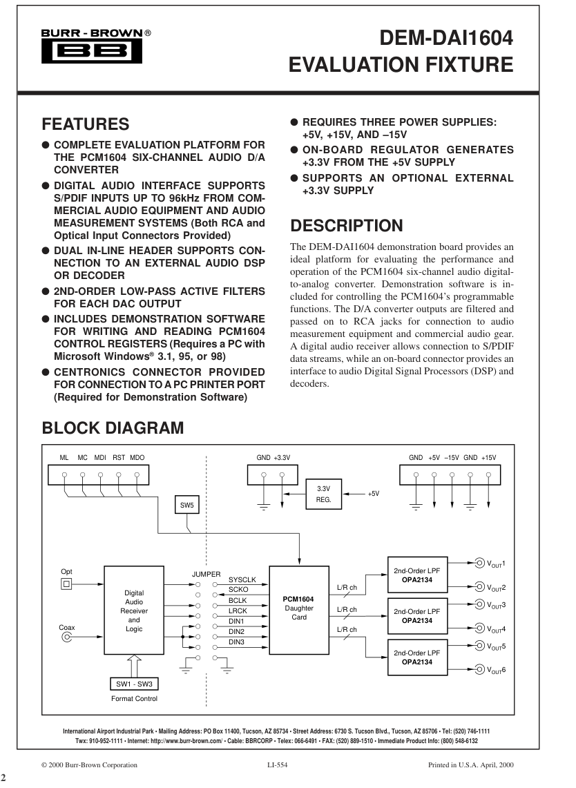
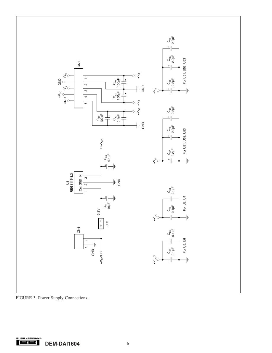
The DEM-DAI1604 requires three external supplies: a +5V supply (VCC) is required for the PCM1604; a digital audio receiver (U3); and associated logic circuitry (U3, U4). An on-board regulator (Burr-Brown REG1117-3.3) is used to generate +3.3V from VCC, which is required by the PCM1604 and associated buffers (U5, U6). The output of the regulator can be disabled by a jumper (JP3) and an external +3.3V supply may then be provided at connector CN4. The op amps used for the low-pass active filters (U50 through U52 ) require positive and negative power supplies. The +VS supply is typically +15V, with a maximum value of +18V and a minimum value of +5V. The –VS supply is
typically –15V, with a minimum value of –18V and a maximum value of –5V. The power supplies used for VCC, +VS, and –VS should be well regulated and filtered. Switching power supplies may be used, but linear regulated supplies are recommended for optimal performance. All supplies should be rated for a minimum of 500mA of output current.
DIGITAL AUDIO INTERFACE
The digital audio interface is provided by a Crystal CS8414 digital audio receiver (U3). The interface is used to receive a stereo, linear PCM, S/PDIF data stream from either an electrical or optical source. The electrical input is furnished by an RCA connector (PJ1), while the optical input is provided by a Toshiba TOSLINK optical receiver (OPT). S/PDIF streams are available from industry standard audio test systems (Audio Precision, Rhode & Schwarz), as well as commercial audio equipment (DVD, CD, and DAT players). The CS8414 outputs a stereo data stream at it’s SDATA pin. This may be used by any or all of the PCM1604’s three data inputs, DIN1 through DIN3. Jumper block JP2 is used to
connect the CS8414 data output to the desired PCM1604 data input pins.
PCM1604 DAUGHTER CARD
The PCM1604 package is soldered directly to a small printed circuit board, referred to as the “daughter card.” The daughter card includes four male connectors which plug into four corresponding female connectors on the DEM- DAI1604 board. The daughter card arrangement is used to provide the best possible dynamic performance, while al- lowing the PCM1604 to be easily interchanged with future multi-channel D/A products.
DAC OUTPUT FILTERS
Three dual op amps (Burr-Brown OPA2134 ) are included to provide 2nd-Order Butterworth low-pass filters for the DAC outputs. These filters are required to attenuate the out-of- band noise generated by the PCM1604’s delta-sigma D/A converters.
PC PRINTER PORT INTERFACE
A Centronics connector is included so that the DEM-DAI1604 may be connected to a PC printer port. The demonstration software included with the DEM-DAI1604 uses this connection to write and read the PCM1604’s internal registers through the MDO, MDI, MC, and ML pins.
CONNECTORS
CN1 is the main power supply connector. Connections for VCC, +VS, –VS, and power supply grounds are provided. CN2 is the zero flag connector. Connector pins ZFLGA and ZFLG1 through ZFLG6 correspond directly to the zero flag output pins of the PCM1604. Alternatively, the zero flag outputs may be used as general purpose logic outputs. CN3 is a Centronics connector used to interface the DEM- DAI1604 to a PC printer port. The +5V logic signals from the printer port are buffered by U6. CN4 is used to connect an optional external +3.3V power supply to the DEM-DAI1604. Typically, this connector is not used since an on-board regulator IC (U8) is used to generate the +3.3V supply. If an external +3.3V supply is
used, remove the jumper at JP3. CN10 through CN13 provide the connection to the PCM1604 daughter board. Figure 1 shows the electrical connections for CN10 through CN13. Figure 4 shows the daughter card schematic. The mapping between the daughter card connectors and CN10 through CN13 is shown in Table I.
| DEM-DAI1604 CONNECTOR | DAUGHTER CARD CONNECTOR |
| CN10 CN11 CN12 CN13 | CN001 CN002 CN003 CN004 |
TABLE I. Daughter Card Connector Mapping.
OPT is the optical receiver input to the CS8414 digital audio receiver. PJ1 is the RCA connector used for shielded cable input to the CS8414 digital audio receiver. PJ2 is the audio output connector corresponding to the PCM1604’s VOUT1 output. PJ3 is the audio output connector corresponding to the PCM1604’s VOUT2 output. PJ4 is the audio output connector corresponding to the PCM1604’s VOUT3 output. PJ5 is the audio output connector corresponding to the PCM1604’s VOUT4 output. PJ6 is the audio output connector corresponding to the PCM1604’s VOUT5 output. PJ7 is the audio output connector corresponding to the PCM1604’s VOUT6 output.
Page 3
SWITCHES
Switches SW1 through SW3 are used to select the audio data output format for the CS8414. Table II shows the output format selections that are used with the PCM1604.
| SW1 | SW2 | SW3 | DATA FORMAT |
| L L H H | L H L H | L L H L | 16-24 Bit Left-Justified, MSB-First(1) 16-24 Bit I2S(2) 16-bit Standard Right-Justified, MSB-First(2) 18-bit Standard Right-Justified, MSB-First(2) |
| NOTE: (1) Jumper JP1 must be set to the INV position when using this format. (2) Jumper JP1 must be set to the NML position when using this format. | |||
TABLE II. Digital Audio Receiver Output Data Format Settings.
| Switch SW5 is used to set the state of the reset (RST) pin of the PCM1604. Table III shows the reset selections. CKS0 and CKS1 are unused and should be set to ‘L’. | |
| RST | MODE OF OPERATION |
| L H | Normal Reset(1) |
| NOTE: (1) The RST pin of the PCM1604 is active LOW. Due to the demo board design, the ‘H’ selection closes the switch and connects RST to ground. The ‘L’ selection opens the switch and the RST pin is set to logic ‘1’ by an internal pull-up resistor. | |
TABLE III. Reset (RST) Operation.
JUMPERS
Jumper JP1 is used to select a non-inverted (NML) or inverted (INV) bit clock for the PCM1604. Table IV shows the proper settings for JP1 for the four input data formats shown in Table II.
| DATA FORMAT | JP1 SELECTION |
| 16 - 24-Bit Left-Justified, MSB-First 16 - 24-Bit I2S 16-Bit, Standard Right-Justified, MSB-First 18-Bit, Standard Right-Justified, MSB-First | INV NML NML NML |
TABLE IV. JP1 Jumper Selection for Audio Data Formats.
Jumper block JP2 is used to connect the digital audio receiver output data and clocks to the PCM1604 daughter card. The jumpers may be removed from JP2 to allow connection to an audio DSP or decoder. Figure 1 shows the electrical connections for JP2. Note that pins DIN1 through DIN3 include 10kΩ pull-down resistors, which may be used to set the data inputs to logic ‘0’ for testing zero detection functions and output cross talk performance. Jumper JP3 is used to enable or disable the on-board +3.3V regulator output. When the jumper is installed, the regulator is used as the +3.3V supply. When it is removed, an external supply, connected at CN4, may be used to supply the +3.3V.
SCHEMATICS
Schematics for the DEM-DAI1604 are shown in Figures 1 through 4. Figure 1 shows the digital audio receiver, associated logic, and digital I/O connectors. Figure 2 shows the DAC low pass filters, while Figure 3 illustrates the power supply connections. Figure 4 shows the PCM1604 daughter card circuitry and connectors.
Page 4
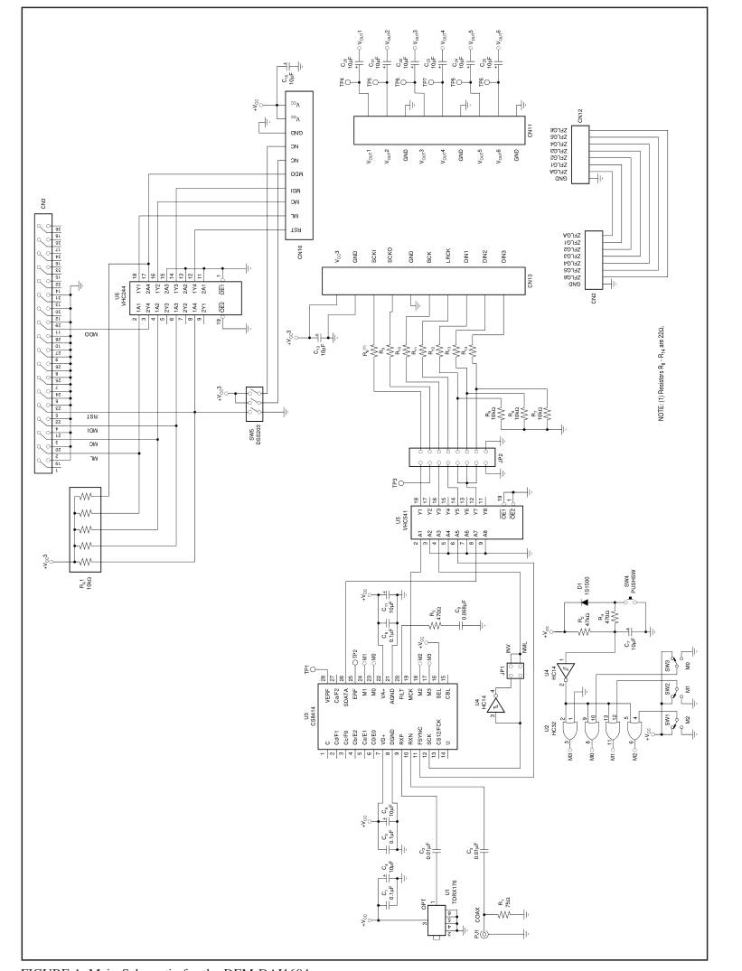
FIGURE 1. Main Schematic for the DEM-DAI1604.
Page 5
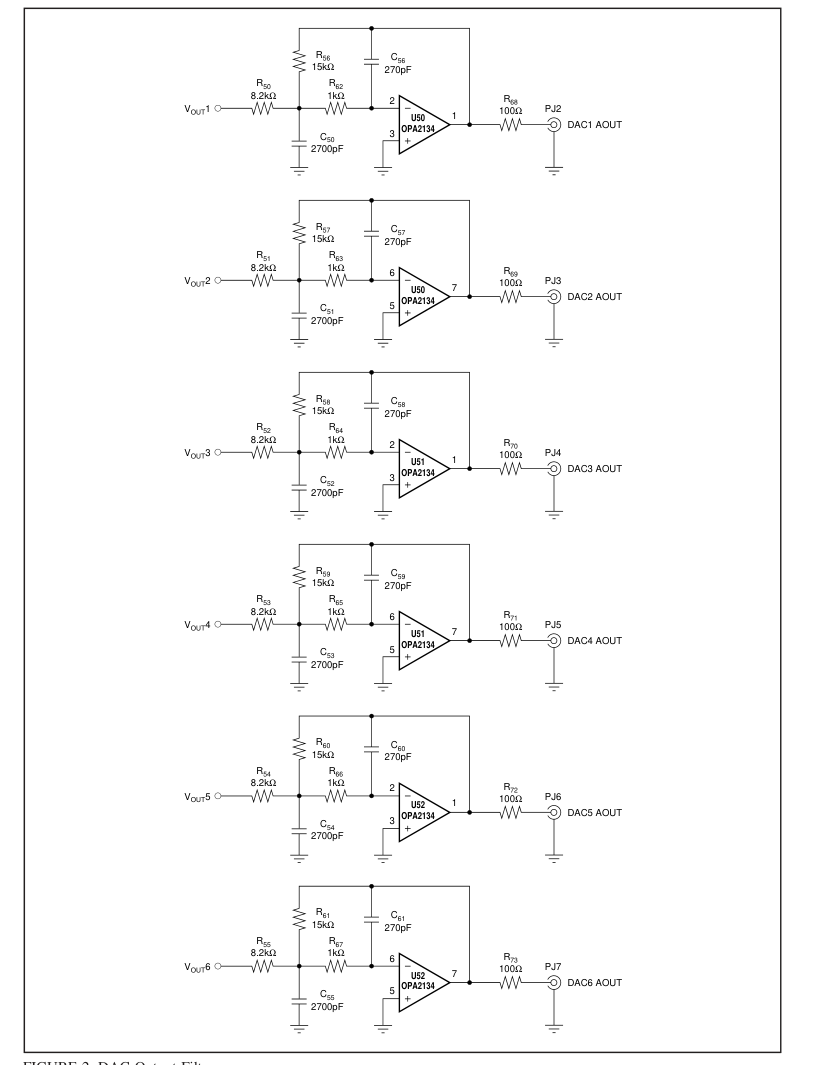
FIGURE 2. DAC Output Filters.
Page 6
Page 7
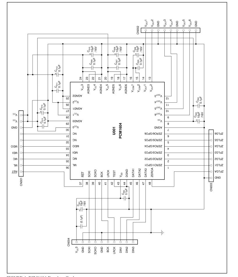
FIGURE 4. PCM1604 Daughter Card.
Page 8
DEMONSTRATION SOFTWARE
Software is provided with the DEM-DAI1604 to allow programming of the PCM1600’s internal registers. The software will operate on computers running Microsoft Windows 3.1, 95 or 98. The demo software requires that the PC printer port be connected to CN3 of the DEM-DAI1604 using a standard printer cable. Installation The demo software is distributed on a 3.5 inch floppy disk. On the disk, there is a single folder named “Dem1604.” This folder contains the application and all support files. To install the software on your computer, first create a new folder on your hard drive with an appropriate name (e.g., DEM1604, PCM1604, etc.). Then open the “Dem1604” folder on the installation floppy and copy all the files in it to
your new folder. Open the configuration settings file named “Dem1604” with a text editor, such as Notepad. When the file is opened, find the following line:
PCMIFADR = &h378
The &h378 indicates the printer port address that the demo software will use to communicate with the DEM-DAI1604. This address must be set to &h378, &h278, or &h3BC. Most PCs use &H378 as the default printer port address. If your printer port is not located at &h378, edit the address to match your computer’s port address. Using the Demo Software Double click on the application file named “Dem1604.” A window will appear on your screen, as shown in Figure 5. There are two menus near the top of the window, named Execute and Window.
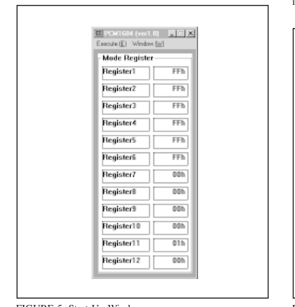
FIGURE 5. Start Up Window.
The Execute menu includes three selections: Initialize, Re- set, and Exit. Selecting Initialize will instruct the program to write all of the PCM1604’s internal registers with the default values. Selecting Reset will instruct the program to rewrite the PCM1604’s internal registers with the data currently selected in the application windows. Selecting Exit will close the application. The Window menu includes four selections: Attenuation, Operational Control, Function Control, and Register Read. The following sections provide an explanation of each window.
HOLD and PASS Each window has a button near the top. It’s labeled either HOLD or PASS. The current setting is toggled by clicking on the button. When set to HOLD, the settings in a window can be changed, but they will not be written to the register(s) until the OK button (which appears at the bottom of the window) is pressed. When set to PASS, setting changes made in a window are immediately written to the corresponding register(s). Attenuation Window The Attenuation window is used to set the digital attenuation registers internal to the PCM1604 and is shown in Figure 6. There is an attenuator for each of the six output channels, and each attenuator has its own independent register to
control its attenuation level. In the Attenuation window, there is a slider for each attenuator register. Use the slider handle or the arrows at each end of the slider to adjust the attenuation level. The left and right arrow keys on the keyboard can also be used to adjust the level. To the right of each slider is a status display showing the current register setting (in decimal) and the corresponding attenuation level in decibels (dB) relative to the input signal level.
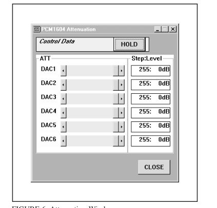
FIGURE 6. Attenuation Window.
Page 9
Although the Attenuation window is used to set the level of the attenuation registers, the actual attenuators inside the PCM1604 will not be updated unless the attenuation load control, ATLD (in the Operational Control window) is set to LOAD. While ATLD is set to OFF, the attenuation registers are written to, but the attenuators are not updated. When ATLD is switched from OFF to LOAD, all attenuators will be updated simultaneously. Operational Control Window The Operational Control window (labeled DAC Operation) is used to program the soft mute (MUT1-6), DAC operation (DAC1-6), attenuation load (ATLD), attenuation rate (ATTS), and infinite zero detect mute (IZD) functions. The mute,
DAC operation, and infinite zero mute functions are set using check boxes, as shown in Figure 7. The labels associated with the check boxes change from ON to OFF as the settings are toggled. The attenuation load and rate functions utilize pull-down menus to set ATLD to Disable or Enable, and ATTS to 2/fS or 4/fS. For more information regarding these functions, please refer to the PCM1604 Product Data Sheet.
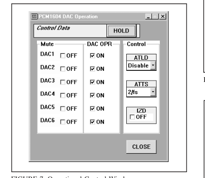
FIGURE 7. Operational Control Window.
Function Control Window The Function window hosts the remainder of the PCM1604 control functions. All functions are programmed using pulldown menus, as shown in Figure 8. Functions that can be programmed by this window include:
- SCLKO Output Enable (CLKE) and Rate (CLKD) Controls
- De-Emphasis Controls (DM12, DM34, DM56) and Sample Rate Selection (DEM)
- Audio Data Format (I/F FORMAT)
- Digital Filter Roll-Off (ROLL-OFF)
- Output Phase (Normal or Inverted)
- Oversampling (64fs or 128fs) These functions are described in detail in the PCM1604 Product Data Sheet.
Register Read Window The PCM1604 serial control interface includes register read capability. The Register Read window (or panel) allows the user to read the value of all PCM1604 registers by pressing a single button. The panel is shown in Figure 9. The Register Read panel provides a means to check for proper communications between the PC printer port and the DEM-DAI1604 by allowing the user to verify register write operations.
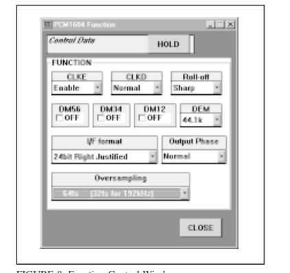
FIGURE 8. Function Control Window.
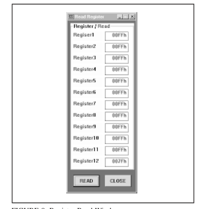
FIGURE 9. Register Read Window.
Page 10
GPO CONTROL WINDOW
The PCM1604 allows the user to select the function of the ZERO1 through ZERO6 output pins. By default, these pins operate as zero flag outputs for VOUT1 through VOUT6 respectively. Control Register 11 allows the user to select an alternate function for these pins. The ZERO1 through ZERO6 pins may be used as general-purpose outputs, or GPO1 through GPO6. When configured as GPO pins, Control Register 12 is utilized to set the output logic level for each pin.
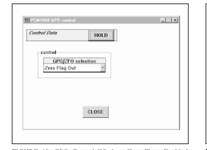
FIGURE 10. GPO Control Window, Zero Flags Enabled
(Default).
. The GPO Control window provides a simple interface for utilizing the PCM1604’s GPO function. Figure 10 shows the default setting of the GPO Control window, where the ZERO1 through ZERO6 output pins are used as zero flags. Figure 11 shows the alternate function, where ZERO1 through ZERO6 are configured as general-purpose logic outputs GPO1 through GPO6. Check boxes are used to set the outputs to the ON (logic 1) or OFF (logic 0) states. The GPO capability is useful for controlling external mute switches, or other digitally-controlled analog circuit functions.
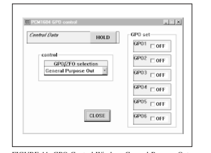
FIGURE 11. GPO Control Window, General Purpose Out-
puts Enabled.
Page 11
IMPORTANT NOTICE
Texas Instruments and its subsidiaries (TI) reserve the right to make changes to their products or to discontinue any product or service without notice, and advise customers to obtain the latest version of relevant information to verify, before placing orders, that information being relied on is current and complete. All products are sold subject to the terms and conditions of sale supplied at the time of order acknowledgment, including those pertaining to warranty, patent infringement, and limitation of liability.
TI warrants performance of its semiconductor products to the specifications applicable at the time of sale in accordance with TI’s standard warranty. Testing and other quality control techniques are utilized to the extent TI deems necessary to support this warranty. Specific testing of all parameters of each device is not necessarily performed, except those mandated by government requirements.
Customers are responsible for their applications using TI components.
In order to minimize risks associated with the customer’s applications, adequate design and operating safeguards must be provided by the customer to minimize inherent or procedural hazards.
TI assumes no liability for applications assistance or customer product design. TI does not warrant or represent that any license, either express or implied, is granted under any patent right, copyright, mask work right, or other intellectual property right of TI covering or relating to any combination, machine, or process in which such semiconductor products or services might be or are used. TI’s publication of information regarding any third party’s products or services does not constitute TI’s approval, warranty or endorsement thereof.
Copyright 2000, Texas Instruments Incorporated