


 Download PDF
DCP010505BP BURR-BROWN
Document overview
- PDF pages: 8
Technical content
Page 1
Page 2
SPECIFICATIONS
At TA = +25°C, unless otherwise specified.
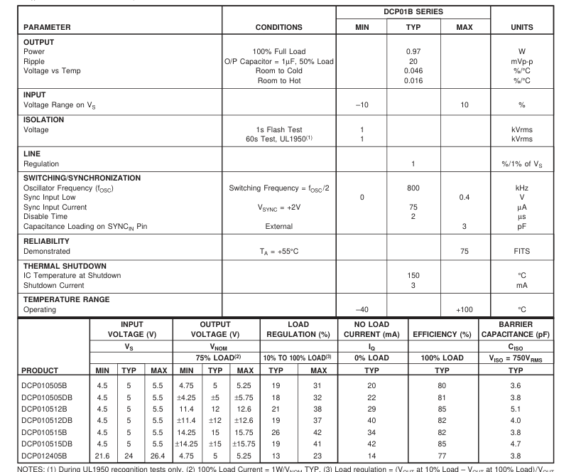
at 75% Load.
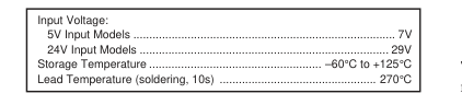
ABSOLUTE MAXIMUM RATINGS
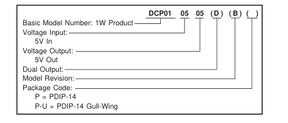
ORDERING INFORMATION
ELECTROSTATIC
DISCHARGE SENSITIVITY
This integrated circuit can be damaged by ESD. Burr-Brown
recommends that all integrated circuits be handled with
appropriate precautions. Failure to observe proper handling
and installation procedures can cause damage. ESD damage can range from subtle performance degrada-
tion to complete device failure. Precision integrated circuits
may be more susceptible to damage because very small
parametric changes could cause the device not to meet its
published specifications.
Page 3
PIN CONFIGURATION (Single-DIP and Gull-Wing)
PIN CONFIGURATION (Dual-DIP and Gull-Wing)
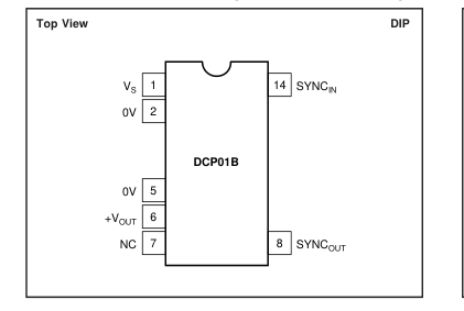
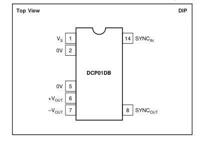
PIN DEFINITION (Single-DIP)
PIN DEFINITION (Dual-DIP)

PACKAGE/ORDERING INFORMATION
| PRODUCT | PACKAGE | PACKAGE DRAWING NUMBER | SPECIFIED TEMPERATURE RANGE | PACKAGE MARKING | ORDERING NUMBER(1) | TRANSPORT MEDIA |
| Single DCP010505BP DCP010505BP-U DCP010512BP DCP010512BP-U DCP010515BP DCP010515BP-U DCP012405BP DCP012405BP-U Dual DCP010505DBP DCP010505DBP-U DCP010512DBP DCP010512DBP-U DCP010515DBP DCP010515DBP-U | DIP-14 DIP-14 Gull-Wing DIP-14 DIP-14 Gull-Wing DIP-14 DIP-14 Gull-Wing DIP-14 DIP-14 Gull-Wing DIP-14 DIP-14 Gull-Wing DIP-14 DIP-14 Gull-Wing DIP-14 DIP-14 Gull-Wing | 010-1 010-2 010-1 010-2 010-1 010-2 010-1 010-2 010-1 010-2 010-1 010-2 010-1 010-2 | –40°C to +100°C –40°C to +100°C –40°C to +100°C –40°C to +100°C –40°C to +100°C –40°C to +100°C –40°C to +100°C –40°C to +100°C –40°C to +100°C –40°C to +100°C –40°C to +100°C –40°C to +100°C –40°C to +100°C –40°C to +100°C | DCP010505BP DCP010505BP-U DCP010512BP DCP010512BP-U DCP010515BP DCP010515BP-U DCP012405BP DCP012405BP-U DCP010505DBP DCP010505DBP-U DCP010512DBP DCP010512DBP-U DCP010515DBP DCP010515DBP-U | DCP010505BP DCP010505BP-U/700 DCP010512BP DCP010512BP-U/700 DCP010515BP DCP010515BP-U/700 DCP012405BP DCP012405BP-U/700 DCP010505DBP DCP010505DBP-U/700 DCP010512DBP DCP010512DBP-U/700 DCP010515DBP DCP010515DBP-U/700 | Rails Tape and Reel Rails Tape and Reel Rails Tape and Reel Rails Tape and Reel Rails Tape and Reel Rails Tape and Reel Rails Tape and Reel |
NOTE: (1) Models with a slash (/) are available only in Tape and Reel in the quantities indicated (e.g., /700 indicates 700 devices per reel). Ordering 700 pieces of “DCP010505BP-U/700” will get a single 700-piece Tape and Reel.
The information provided herein is believed to be reliable; however, BURR-BROWN assumes no responsibility for inaccuracies or omissions. BURR-BROWN assumes no responsibility for the use of this information, and all use of such information shall be entirely at the user’s own risk. Prices and specifications are subject to change without notice. No patent rights or licenses to any of the circuits described herein are implied or granted to any third party. BURR-BROWN does not authorize or warrant any BURR-BROWN product for use in life support devices and/or systems.
Page 4
TYPICAL PERFORMANCE CURVES
At TA = +25°C, unless otherwise noted.
DCP010505B OUTPUT RIPPLE vs LOAD (20MHz BW)
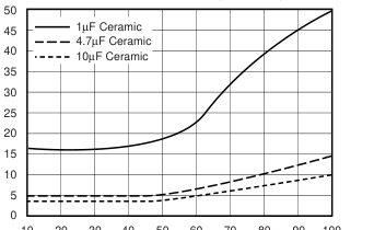
10 20 30 40 50 60 70 80 90 100
Load (%)
DCP010505B VOUT vs LOAD
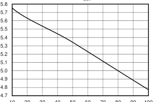
10 20 30 40 50 60 70 80 90 100
Load (%)
DCP010505DB VOUT vs LOAD
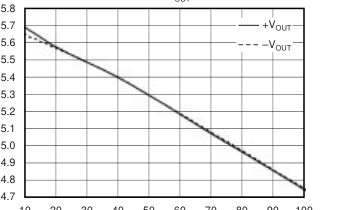
10 20 30 40 50 60 70 80 90 100
Load (%)
DCP010505B VOUT vs VS
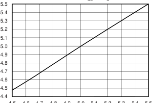
4.5 4.6 4.7 4.8 4.9 5.0 5.1 5.2 5.3 5.4 5.5
VS (V)
DCP010505B EFFICIENCY vs LOAD
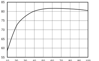
10 20 30 40 50 60 70 80 90 100
Load (%)
DCP010505DB EFFICIENCY vs LOAD
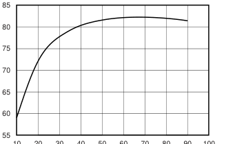
10 20 30 40 50 60 70 80 90 100
Load (%)
Page 5
TYPICAL PERFORMANCE CURVES (Cont.)
At TA = +25°C, unless otherwise noted.
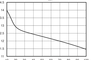
DCP010512B VOUT vs LOAD
10 20 30 40 50 60 70 80 90 100
Load (%)
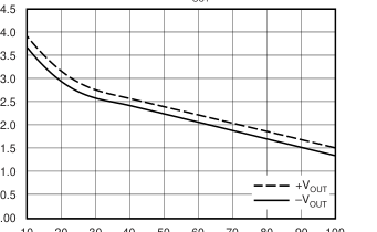
DCP010512DB VOUT vs LOAD
10.00 10 20 30 40 50 60 70 80 90 100
Load (%)
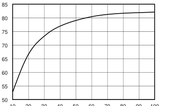
DCP010515B EFFICIENCY vs LOAD
10 20 30 40 50 60 70 80 90 100
Load (%)
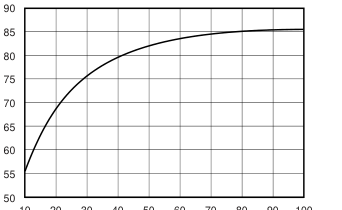
DCP010512B EFFICIENCY vs LOAD
10 20 30 40 50 60 70 80 90 100
Load (%)
DCP010512DB EFFICIENCY vs LOAD
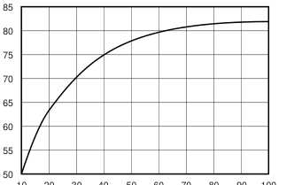
10 20 30 40 50 60 70 80 90 100
Load (%)
DCP010515B VOUT vs LOAD
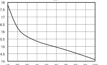
10 20 30 40 50 60 70 80 90 100
Load (%)
Page 6
TYPICAL PERFORMANCE CURVES (Cont.)
At TA = +25°C, unless otherwise noted.
DCP010515DB VOUT vs LOAD
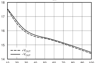
10 20 30 40 50 60 70 80 90 100
Load (%)
DCP012405B VOUT vs LOAD
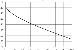
10 20 30 40 50 60 70 80 100
Load (%)
DCP010505B CONDUCTED EMISSIONS (125% Load)
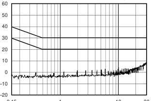
0.15
1
10 30
Frequency (MHz)
DCP010515DB EFFICIENCY vs LOAD
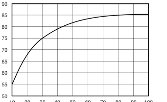
10 20 30 40 50 60 70 80 90 100
Load (%)
DCP012405B EFFICIENCY vs LOAD
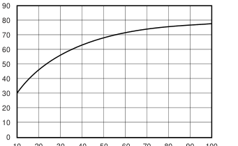
10 20 30 40 50 60 70 80 90 100
Load (%)
DCP010505B CONDUCTED EMISSIONS (8% Load)
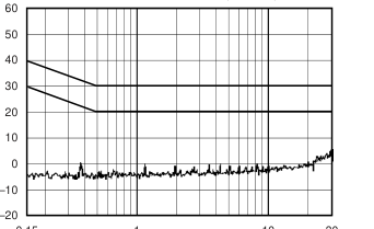
0.15
1
10 30
Frequency (MHz)
Page 7
FUNCTIONAL DESCRIPTION
OVERVIEW
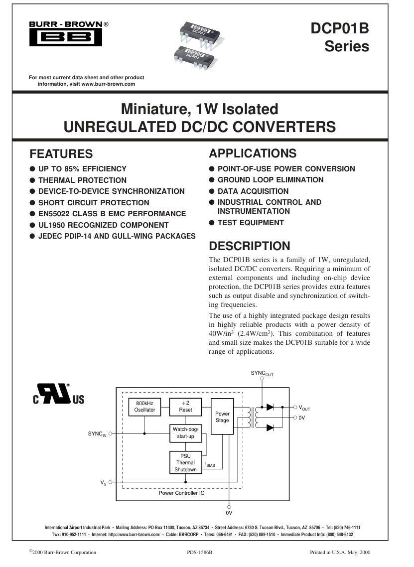
The DCP01B offers up to 1W of unregulated output power with a typical efficiency of up to 85%. This is achieved through highly integrated packaging technology and the implementation of a custom power stage and control IC. The circuit design utilizes an advanced BiCMOS/DMOS process.
POWER STAGE
This uses a push-pull, center-tapped topology switching at 400kHz (divide by 2 from 800kHz oscillator).
OSCILLATOR AND WATCHDOG
The onboard 800kHz oscillator generates the switching frequency via a divide by 2 circuit. The oscillator can be synchronized to other DCP01B circuits or an external source, and is used to minimize system noise. A watchdog circuit checks the operation of the oscillator circuit. The oscillator can be stopped by pulling the SYNC pin LOW. The output pins will be tri-stated. This will occur in 2µs.
THERMAL SHUTDOWN
The DCP01B is protected by a thermal shutdown circuit. If the on-chip temperature exceeds 150°C, the device will shut down. Once the temperature falls below 150°C, normal operation will resume.
SYNCHRONIZATION
In the event that more than one DC/DC converter is needed onboard, beat frequencies and other electrical interference can be generated. This is due to the small variations in switching frequencies between the DC/DC converters. The DCP01B overcomes this by allowing devices to be synchronized to one another. Up to eight devices can be synchronized by connecting the SYNCIN pins together, taking care to minimize the capacitance of tracking. Stray capacitance (> 3pF) will have the effect of reducing the switching frequency, or even stopping the oscillator circuit.
If synchronized devices are used, it should be noted that, at start up, all devices will draw maximum current simultaneously. This can cause the input voltage to dip and should it dip below the minimum input voltage (4.5V), the devices may not start up. A 2.2µF capacitor should be connected close to the input pins. If more than eight devices are to be synchronized, it is recommended that the SYNCIN pins are driven by an external device. Details are contained in a separate applications bulletin (AB-153).
CONSTRUCTION
The DCP01B’s basic construction is the same as standard ICs. There is no substrate within the molded package. The DCP01B is constructed using an IC, rectifier diodes, and a wound magnetic toroid on a leadframe. As there is no solder within the package, the DCP01B does not require any special PCB assembly processing. This results in an isolated DC/DC converter with inherently high reliability.
ADDITIONAL FUNCTIONS
DISABLE/ENABLE
The DCP01B can be disabled or enabled by driving the SYNC pin using an open drain CMOS gate. If the SYNCIN pin is pulled low, the DCP01B will be disabled. The disable time depends upon the external loading; the internal disable function is implemented in 2µs. Removal of the pull down will cause the DCP01B to be enabled. Capacitive loading on the SYNCIN pin should be minimized in order to prevent a reduction in the oscillator frequency.
DECOUPLING
Ripple Reduction The high switching frequency of 400kHz allows simple filtering. To reduce ripple, it is recommended that at least a 1µF capacitor is used on VOUT. Dual outputs should both be decoupled to pin 5. A 2.2µF low ESR capacitor on the input of the 5V in versions, and a 0.47µF low ESR cap on the 24V DCP01B in versions is recommended.
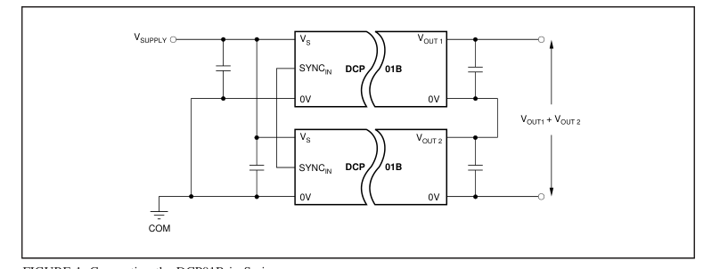
FIGURE 1. Connecting the DCP01B in Series.
Page 8
Connecting the DCP01B in Series Multiple DCP01B isolated 1W DC/DC converters can be connected in series to provide nonstandard voltage rails. This is possible by utilizing the floating outputs provided by the DCP01B’s galvanic isolation. Connect the positive VOUT from one DCP01B to the negative VOUT (0V) of another (see Figure 1). If the SYNCIN pins are tied together, the self-synchronization feature of the DCP01B will prevent beat frequencies on the voltage rails. The SYNCIN feature of the DCP01B allows easy series connection without external filtering, minimizing cost. The outputs on dual output DCP01B versions can also be connected in series to provide two times the magnitude of
VOUT as shown in Figure 2. For example, a dual 15V DCP01B could be connected to provide a 30V rail. Connecting the DCP01B in Parallel If the output power from one DCP01B is not sufficient, it is possible to parallel the outputs of multiple DCP01Bs, as shown in Figure 3. Again, the SYNCIN feature allows easy synchronization to prevent power-rail beat frequencies at no additional filtering cost.
PCB LAYOUT
Ripple and Noise Careful consideration should be given to the layout of the PCB in order that the best results can be obtained.
The DCP01B is a switching power supply and as such can place high peak current demands on the input supply. In order to avoid the supply falling momentarily during the fast switching pulses ground and power planes should be used to track the power to the input of DCP01B. If this is not possible then the supplies must be connected in a star formation with the tracks made as wide as possible. If the SYNCIN pin is being used then the tracking between device SYNCIN pins should be short to avoid stray capacitance. If the SYNCIN pin is not being used it is advisable to place a guard ring, (connected to input ground) around this pin to avoid any noise pick up.
The output should be taken from the device using ground and power planes, this will ensure minimum losses. A good quality low ESR capacitor placed as close as practicable across the input will reduce reflected ripple and ensure a smooth start up. A good quality low ESR capacitor placed as close as practicable across the rectifier output terminal and output ground will give the best ripple and noise performance.
THERMAL MANAGEMENT
Due to the high power density of this device it is advisable to provide ground planes on the input and output.
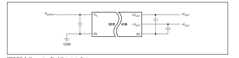
FIGURE 2. Connecting Dual Outputs in Series.
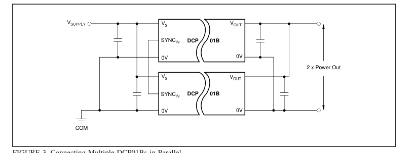
FIGURE 3. Connecting Multiple DCP01Bs in Parallel.