

 Download PDF
DBW WALL
Document overview
- PDF pages: 4
Technical content
Page 1
APPLICATIONS
FEATURES
- Telecom/Datacom
- High Efficiency up to 88%
- Wireless Networks
- RoHS Directive Compliant
- Measurement Equipment
- Fixed Switching Frequency
- Industry Control Systems
- Six-Sided Continuous Shield
- Semiconductor Equipment
- Standard 2” x 2” x 0.4” Package
- Options: Negative Remote ON/OFF
- 4:1 Ultra Wide Input Voltage Range
- ISO9001 Certified Manufacturing Facilities
UL
- UL60950-1, EN60950-1, and IEC60950-1 Licensed
TUV
- CE Mark Meets 2006/95/EC, 93/68/EEC, and 2004/108/EC
CB
CE MARK
DESCRIPTION
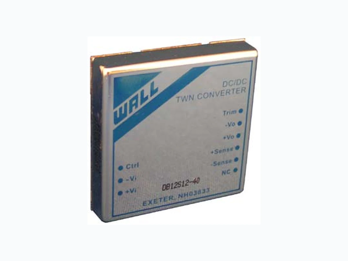
The DBW series of DC/DC converters offers 40 Watts of output power in a 2 x 2 x 0.4 inch package. The DBW series has a 4:1 ultra wide input range of 9-36VDC or 18-75VDC. This series also offers single and dual output models. Some features include 1600VDC isolation, positive or negative remote on/off, and six-sided shielding. All models are short circuit, over voltage, over load, and over temperature protected. Heatsinks are also available, please call factory for ordering details.
SPECIFICATIONS: DBW Series
All specifications apply @ 25°C ambient unless otherwise noted
INPUT SPECIFICATIONS
Input Voltage Range ............ 24V nominal input ........................ 9 - 36VDC
48V nominal input ...................... 18 - 75VDC
Input Filter ....................................................................................... Pi Type Input Surge Voltage (100ms max) ............... 24V input ...................50VDC
48V input .................100VDC
Input Reflected Ripple Current (nominal Vin and FL) ...................20mAp-p Start Up Time (nominal Vin and constant resistive load) Power Up.............................................................................20ms, max. Remote ON/OFF .................................................................20ms, max. Start-Up Voltage .................. 24V nominal input ................................9VDC
48V nominal input ..............................18VDC
Shutdown Voltage................ 24V nominal input ................................8VDC
48V nominal input ..............................16VDC
Remote ON/OFF (See Note 10) Positive Logic ................. DC-DC ON................Open or 3V < Vr < 12V
DC-DC OFF .............Short or 0V < Vr < 1.2V
Negative Logic................ DC-DC ON...............Short or 0V < Vr < 1.2V
DC-DC OFF ..............Open or 3V < Vr < 12V
Input Current of Remote Control Pin (nominal Vin) ..........-0.5mA~+0.5mA Remote Off State Input Current ........... 24V nominal input................10mA
48V nominal input..................5mA
OUTPUT SPECIFICATIONS
Output Voltage ..............................................................................see table Voltage Accuracy (nom Vin and full load)........................................... ±1% Voltage Adjustability (See Note 7) ..................................................... ±10% Output Current ..............................................................................see table Output Power ....................................................................... 40 watts, max. Line Regulation (LL to HL at FL)....................................................... ±0.2% Load Regulation (See Note 8) ..................... Single Output............. ±0.5%
(min. load to full load)
Dual Output ................... ±1%
Load Cross Regulation (See Note 9)........... Dual Output ................... ±5% Minimum Load (See Note 6) .........................................................see table Ripple/Noise (See Note 4) ............................................................see table Transient Response Recovery Time................................................. 250µs (25% load step change)
PROTECTION SPECIFICATIONS
Over Voltage Protection ...................................3.3V Output.................3.9V (Zener diode clamp)
5V Output....................6.2V 12V Output...................15V 15V Output...................18V ±12V Output...............±15V ±15V Output...............±18V
Over Load Protection (% of FL at nominal input) ...................... 150%, max. Short Circuit Protection......................................Hiccup, automatic recovery Over Temperature Protection......................................................110°C, typ.
GENERAL SPECIFICATIONS
Efficiency ........................................................................................see table Switching Frequency ................................................................300KHz, typ. Isolation Voltage Input to Output..................................................................1600VDC, min. Input to Case ....................................................................1600VDC, min. Output to Case..................................................................1600VDC, min. Case Grounding .......................connect case to -Vin with decoupling Y cap Isolation Resistance .....................................................................109Ω, min.
Isolation Capacitance ............................................................ 2500pF, max.
ENVIRONMENTAL SPECIFICATIONS
Operating Ambient Temperature............. -40°C to +50°C (without derating)
+50°C to +105°C (with derating)
Storage Temperature ..........................................................-55°C ~ +125°C Maximum Case Temperature........................................................... +105°C Relative Humidity...................................................................5% to 95% RH Temperature Coefficient.................................................. ±0.02% / °C, max. Thermal Impedance (See Note 11) Without Heat-Sink..............................................................9.2°C / Watt With Heat-Sink...................................................................7.6°C / Watt Thermal Shock ..................................................................... MIL-STD-810F
Vibration ................................................................................MIL-STD-810F MTBF (See Note 1) ........Bellcore TR-NWT-000332............ 1.105 x 10⁶ hrs
MIL-STD-217F ............................. 1.511 x 10⁵ hrs
Page 1 of 4
Page 2
Due to advances in technology, specifications subject to change without notice
MODEL SELECTION CHART
| Model Number | Input Range | Output Voltage | Output Current | Output(4) Ripple & Noise | Input Current | Efficiency(4) | Max Capacitive Load(5) | ||
|---|---|---|---|---|---|---|---|---|---|
| Min. Load(6) | Full Load | No Load(3) | Full Load(2) | ||||||
| DBW24S3.3-33 | 24VDC (9 – 36 VDC) | 3.3 VDC | 0mA | 10,000mA | 50mVp-p | 80mA | 1677mA | 86% | 25,750μF |
| DBW24S5-40 | 5 VDC | 0mA | 8000mA | 50mVp-p | 100mA | 2008mA | 87% | 13,600μF | |
| DBW24S12-40 | 12 VDC | 50mA | 3333mA | 75mVp-p | 50mA | 2008mA | 87% | 2360μF | |
| DBW24S15-40 | 15 VDC | 50mA | 2666mA | 75mVp-p | 50mA | 2008mA | 87% | 1510μF | |
| DBW24D12-40 | ±12 VDC | ±65mA | ±1667mA | 120mVp-p | 60mA | 2032mA | 86% | ±1200μF | |
| DBW24D15-40 | ±15 VDC | ±50mA | ±1333mA | 150mVp-p | 70mA | 2032mA | 86% | ±750μF | |
| DBW48S3.3-33 | 48VDC (18 – 75 VDC) | 3.3 VDC | 0mA | 10,000mA | 50mVp-p | 60mA | 838mA | 86% | 25,750μF |
| DBW48S5-40 | 5 VDC | 0mA | 8000mA | 50mVp-p | 65mA | 992mA | 88% | 13,600μF | |
| DBW48S12-40 | 12 VDC | 50mA | 3333mA | 75mVp-p | 30mA | 1004mA | 87% | 2360μF | |
| DBW48S15-40 | 15 VDC | 50mA | 2666mA | 75mVp-p | 30mA | 1004mA | 87% | 1510μF | |
| DBW48D12-40 | ±12 VDC | ±65mA | ±1667mA | 120mVp-p | 30mA | 1016mA | 86% | ±1200μF | |
| DBW48D15-40 | ±15 VDC | ±60mA | ±1333mA | 150mVp-p | 30mA | 1016mA | 86% | ±750μF | |
NOTES
- BELLCORE TR-NWT-000332. Case I: 50% Stress, Temperature at 40ºC. MIL-STD-217F Notice2 @ Ta=25°C, Full Load (Ground, Benign, controlled environment). 2. Maximum value at nominal input voltage and full load. 3. Typical Value at nominal input voltage and no load. 4. Typical Value at nominal input voltage and full load. 5. Test by minimum Vin and constant resistive load. 6. The output requires a minimum loading on the output to maintain specified regulations. Operation under no-load conditions will not damage these devices, however they may not meet all listed specifications. 7. For single output models: maximum output deviation is 10% inclusive of remote sense and trim. If remote sense is not being used the
+SENSE should be connected to the +OUTPUT and the -SENSE should be connected to the –OUTPUT. 8. Load regulation for dual output: Minimum load to 100% load balanced on all outputs. 9. Cross regulation for dual output: asymmetrical load 25% / 100% full load. 10. The ON/OFF control function: There are positive (standard) and negative logic (option). The pin voltage is referenced to negative input. To order negative logic ON/OFF control add the suffix “R” to the part number (Ex: DBW48S5-40R). 11. Heat sink is optional. Please call factory for ordering details. 12. The DBW series can meet EN55022 Class A with an external capacitor in parallel with the input pins.
Recommended: 24Vin: N/A.
48Vin: 2.2µF/100V \* 2 PCS 1812 MLCC.
- An external input filter capacitor is required if the module has to meet EN61000-4-4, EN61000-4-5. The filter capacitor suggested is Nippon chemi-con KY series, 220µF/100V, ESR 48mΩ.
Page 2 of 4
Page 3
DERATING CURVES & EFFICIENCY GRAPHS
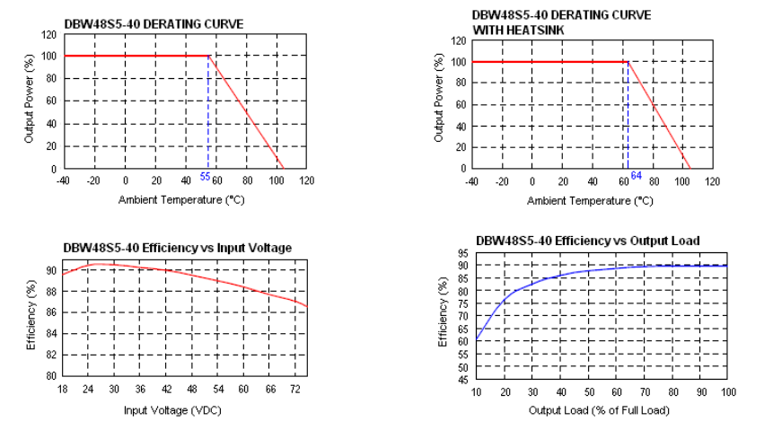
Figure 2
Figure 1
Recommended Filter for EN55022 Class B Compliance
Recommended EN55022 Class B Filter Circuit Layout
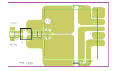
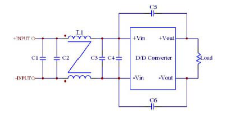
The components used in the above figure are as follows:
| C1 | C2 | C3 | C4 | C5 & C6 | L1 | |
| DBW24Sxx-xx | 4.7µF/50V 1812MLCC | N/A | 4.7µF/50V 1812MLCC | N/A | 1000pF/2KV MLCC | 450µH Common Choke PMT-048 |
| DBW48Sxx-xx | 2.2µF/100V 1812 MLCC | 2.2µF/100V 1812 MLCC | 2.2µF/100V 1812 MLCC | 2.2µF/100V 1812 MLCC | 1000pF/2KV MLCC | 830µH Common Choke PMT-053 |
Page 3 of 4
Page 4
MECHANICAL DRAWING
Unit: inches (mm)
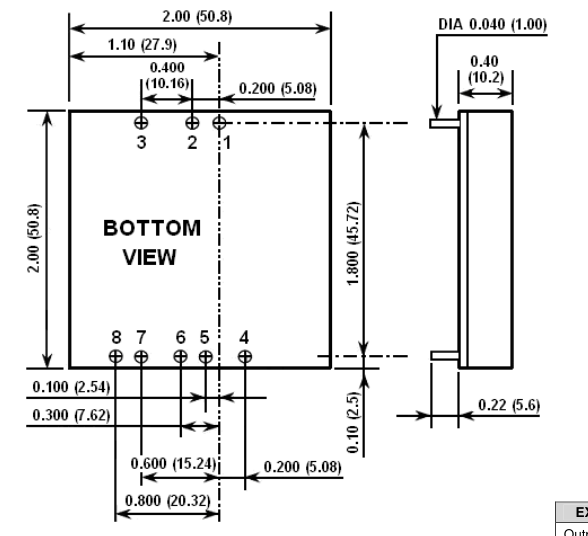
| PIN CONNECTION | ||
| PIN | SINGLE | DUAL |
| 1 | +Input | +Input |
| 2 | -Input | -Input |
| 3 | CTRL | CTRL |
| 4 | -Sense | +Output |
| 5 | +Sense | COM |
| 6 | +Output | COM |
| 7 | -Output | -Output |
| 8 | Trim | Trim |
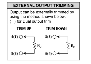
Notes 1. Tolerance: X.XX±0.02 (X.X±0.5) X.XXX±0.01 (X.XX±0.25) 2. Pin pitch tolerance: ±0.01 (0.25) 3. Pin dimension tolerance: ±0.004 (0.1)
Page 4 of 4