
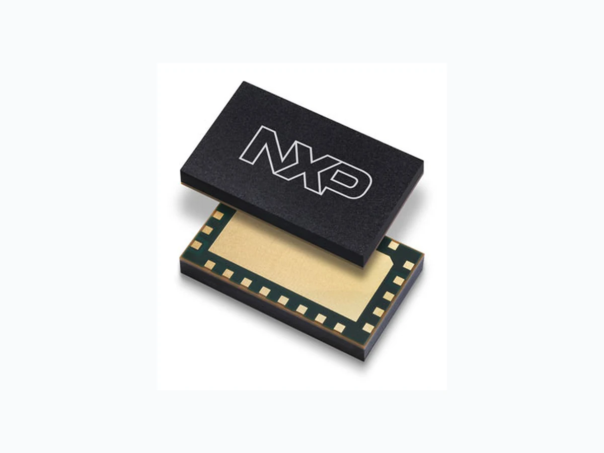
A5M36TG140 NXP
Document overview
- Manufacturer or author: NXP Semiconductors
- PDF pages: 17
Technical content
Features
- 2−stage module solution that includes an LDMOS integrated circuit as a driver and a GaN final stage amplifier
- Advanced high performance in−package Doherty
- Fully matched (50 ohm input/output, DC blocked)
- Designed for low complexity digital linearization systems
- Reduced memory effects for improved linearized error vector magnitude Data Sheet: Technical Data A5M36TG140 Airfast Power Amplifier Module Rev. 1 — January 2023 3300–3800 MHz, 32 dB, 9 W Avg. AIRFAST POWER AMPLIFIER MODULE A5M36TG140 10 mm /C01216 mm Module NXP reserves the right to change the detail specifications as may be required to permit improvements in the design of its products.
Figure 1. Pin Connections Note: Exposed backside of the package is DC and RF ground.
- V DP2 and VDC2 are DC coupled internal to the package and must be powered by a single DC power supply.
Table 1. Functional Pin Description
3 VDP2 Peaking Drain Supply, Stage 2
4 VDP1 Peaking Drain Supply, Stage 1
5 RFin RF Input
6 VGP2 Peaking Gate Supply, Stage 2
7 VGP1 Peaking Gate Supply, Stage 1
8 VGC1 Carrier Gate Supply, Stage 1
9 VGC2 Carrier Gate Supply, Stage 2
10 VDC1 Carrier Drain Supply, Stage 1
11 VDC2 Carrier Drain Supply, Stage 2
17 RFout RF Output
Figure 2. Functional Electrical Routing Diagram
Table 2. Maximum Ratings Table 3. Lifetime Table 4. Thermal Characteristics Table 5. ESD Protection Characteristics Table 6. Moisture Sensitivity Level
- R θCHC (FEA) must be used for purposes related to reliability and limitations on maximum channel temperature. MTTF may be estimated
by the expression MTTF (hours) = 10[A + B/(T + 273)], where T is the channel temperature in degrees Celsius, A = –11.6 and B = 9129.
- Simulated maximum FEA channel−to−case thermal resistance: 10.7°C/W, PD = 9.4 W.
Table 7. Electrical Characteristics (TA = 25°C unless otherwise noted)
- Carrier side and Peaking side are tied together for these measurements.
Table 7. Electrical Characteristics (TA = 25°C unless otherwise noted) (continued) ISBW of 400 MHz at 55 Vdc, 3 dB Input Overdrive from 9 W Avg. Table 8. Ordering Information
- Part input and output matched to 50 ohms.
- ATE is a socketed test environment.
- Increase V GP2 (peaking side) until IDQP2 = 35 mA current is attained, and then subtract 1.3 V for final VGP2 bias voltage.
- All data measured in fixture with device soldered in NXP reference circuit.
GP2 (peaking side) until IDQP2 = 35 mA current is attained, and then subtract 1.0 V for final VGP2 bias voltage.
- Gain flatness = Max(G(f Low to fHigh)) – Min(G(fLow to fHigh))
Data Sheet: Technical Data 7 / 17 A5M36TG140 Airfast Power Amplifier Module, Rev. 1, January 2023 Correct Biasing Sequence Turn ON: Bias ON the GaN final stage first 1. Set gate voltage V GC2 and VGP2 to –5 V. 2. Set drain voltage V DC2 and VDP2 to nominal supply voltage (+48 V). 3. Increase V GP2 (peaking side) until IDQP2 = 35 mA current is attained, and then subtract 1.0 V for final VGP2 bias voltage. 4. Increase V GC2 (carrier side) until IDQC2 current is attained. Bias ON the LDMOS driver stage second 5. Set drain voltage V DC1 and VDP1 to nominal supply voltage (+5 V). 6. Increase V GC1 (carrier side) until IDQC1 current is attained. 7. Increase V GP1 (peaking side) until IDQP1 current is attained. 8. Apply RF input power to desired level. Turn OFF: Bias OFF the GaN final stage first 1. Disable RF input power. 2. Adjust gate voltage VGC2 and VGP2 to –5 V. 3. Adjust drain voltage VDC2 and VDP2 to 0 V. Allow adequate time for drain voltage to reduce to 0 V from external drain capacitors. 4. Disable V GC2 and VGP2. Bias OFF the LDMOS driver stage second 5. Adjust gate voltage VGC1 and VGP1 to 0 V. 6. Adjust drain voltage VDC1 and VDP1 to 0 V.
Figure 3. A5M36TG140 Reference Circuit Component Layout Table 9. A5M36TG140 Reference Circuit Component Designations and Values Note: Component numbers C5, C8 and R7 are intentionally omitted.
Figure 4. Product Marking
Data Sheet: Technical Data 10 / 17 A5M36TG140 Airfast Power Amplifier Module, Rev. 1, January 2023
Package Information
Data Sheet: Technical Data 11 / 17 A5M36TG140 Airfast Power Amplifier Module, Rev. 1, January 2023
Data Sheet: Technical Data 12 / 17 A5M36TG140 Airfast Power Amplifier Module, Rev. 1, January 2023
Data Sheet: Technical Data 13 / 17 A5M36TG140 Airfast Power Amplifier Module, Rev. 1, January 2023
Data Sheet: Technical Data 14 / 17 A5M36TG140 Airfast Power Amplifier Module, Rev. 1, January 2023
Data Sheet: Technical Data 15 / 17 A5M36TG140 Airfast Power Amplifier Module, Rev. 1, January 2023
Data Sheet: Technical Data 16 / 17 A5M36TG140 Airfast Power Amplifier Module, Rev. 1, January 2023 Product Documentation and Tools Refer to the following resources to aid your design process. Application Notes
- AN1955: Thermal Measurement Methodology of RF Power Amplifiers Development Tools
- Printed Circuit Boards Failure Analysis At this time, because of the physical characteristics of the part, failure analysis is limited to electrical signature analysis. In cases where NXP is contractually obligated to perform failure analysis (FA) services, full FA may be performed by third party vendors with moderate success. For updates contact your local NXP Sales Office.
Revision History
The following table summarizes revisions to this document. Revision Date Description 0 Oct. 2022 • Initial release of data sheet 1 Jan. 2023 • Maximum Ratings table, Maximum Forward Gate Current value: updated to reflect device periphery, p. 4
- Thermal Characteristics table, Thermal Resistance Channel−to−Case: updated to include both typical and maximum FEA simulated values, p. 4
- Typical Performance table, 1−carrier 20 MHz LTE, ALT2: updated Typ value to reflect test data, p. 6
- Typical Performance table, Pulsed CW, 10% Duty Cycle Typ values: updated to reflect test data, p. 6
Data Sheet: Technical Data 17 / 17 A5M36TG140 Airfast Power Amplifier Module, Rev. 1, January 2023 Information in this document is provided solely to enable system and software implementers to use NXP products. There are no express or implied copyright licenses granted hereunder to design or fabricate any integrated circuits based on the information in this document. NXP reserves the right to make changes without further notice to any products herein. NXP makes no warranty, representation, or guarantee regarding the suitability of its products for any particular purpose, nor does NXP assume any liability arising out of the application or use of any product or circuit, and specifically disclaims any and all liability, including without limitation consequential or incidental damages. “Typical” parameters that may be provided in NXP data sheets and/or specifications can and do vary in different applications, and actual performance may vary over time. All operating parameters, including “typicals,” must be validated for each customer application by customer’s technical experts. NXP does not convey any license under its patent rights nor the rights of others. NXP sells products pursuant to standard terms and conditions o f sale, which can be found at the following address: nxp.com/SalesTermsandConditions. NXP , the NXP logo and Airfast are trademarks of NXP B.V. All other product or service names are the property of their respective owners. How to Reach Us Home Page: nxp.com Web Support: nxp.com/support /C0069 NXP B.V. 2022–2023 All rights reserved. For more information, please visit: http://www.nxp.com For sales office addresses, please send an email to: salesaddresses@nxp.com Date of release: January 2023 Document identifier: A5M36TG140