
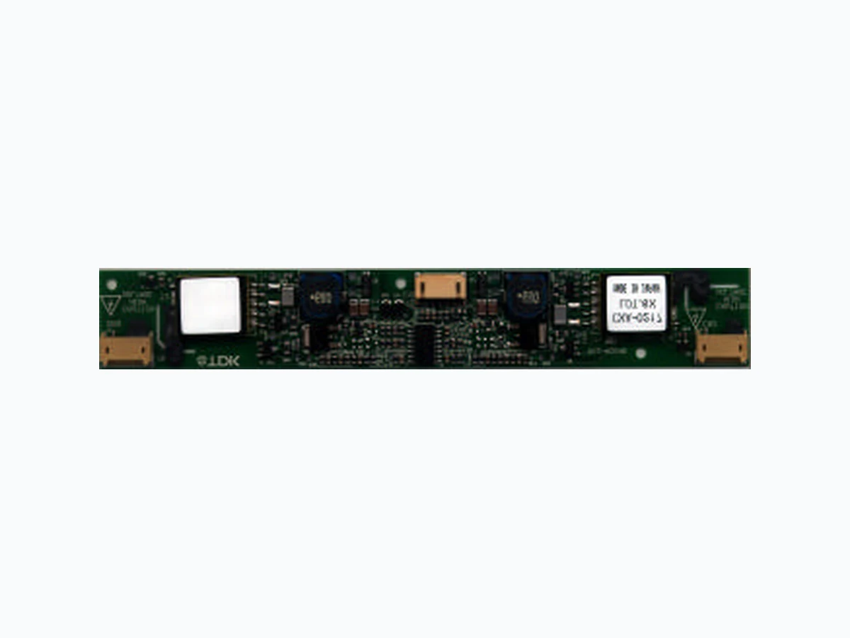
CXA-0217 POWER-SYSTEMS
Document overview
- Manufacturer or author: Provided By www.digicamel.com(FREE DATASHEET DOWNLOAD SITE)
- PDF pages: 4
Technical content
CXA-0217 (CXA -P1212-VJL) (7W DUAL OUTPUTS WITH DIMMING FUNCTION) DC-AC INVERTER UNIT (PRELIMINARY INFORMATION) Power Systems – The Power Solution Web: www.Power-Systems.de Address: Dörnet 8 ; 74360 Ilsfeld -Auenstein / Germany Email: Info@Power-Systems.de Tel. : + 49 / 70 62 / 67 59 - 6 Fax: + 49 / 70 62 / 67 59 - 80 All specification are subject to change without notice. Page ( 1 / 4 ) VER, 16 December 2002 DESCRIPTION : This DC to AC Inverter was developed for large size LCD panel as Multiple Media, Replacement of CRT Monitor and other general Purpose. APPLICABLE LCD: 11 to 14 inches Double lamps type Lamp Voltage 660V Lamp Current 6mA FEATURES : Current Feedback Circuit High Efficiency Low noise with voltage resonant circuit Regulated output current Output Current Feedback Circuit for each Lamp 8mm Low Profile. TEMPERATURE & HUMDITY : Operating Temperature Range 0 °C ~ +70 °C Storage Temperature Range -30 °C ~ +85 °C Humidity 95 %RH max DIMENSIONS : 8 max 180.0 ± 0,5 25.0 ± 0.3 Unit : mm Weight : 30 (g) typ. 3-φ 3±0.2 CN1 18 ± 0.2 146.5 ±0.2 2 3 CN3 CN2 No. Part Discription Qty. Material Note
1 PCB 1 UL94V-0 (FR-4 or CEM-3) t=1mm
2 Connector CN1 1 S5B-PH-SM3 JST
3 Connector CN2 1 SM02(8.0)B-BHS-1 JST 4 Connector CN3 1 SM02(8.0)B-BHS-1 JST
CXA-0217 (CXA -P1212-VJL) (7W DUAL OUTPUTS WITH DIMMING FUNCTION) DC-AC INVERTER UNIT (PRELIMINARY INFORMATION) Power Systems – The Power Solution Web: www.Power-Systems.de Address: Dörnet 8 ; 74360 Ilsfeld -Auenstein / Germany Email: Info@Power-Systems.de Tel. : + 49 / 70 62 / 67 59 - 6 Fax: + 49 / 70 62 / 67 59 - 80 All specification are subject to change without notice. Page ( 2 / 4 ) VER, 16 December 2002 ELECTRICAL CHARACTERISTICS : Pin No. Symbols Ratings CN 1-1 Vin 9.6-14.4V CN 1-2 GND 0V CN 1-3 Vbr 0~3,4V CN 1-4 - N.C. CN 1-5 Vrmt Input 5V 0~0.4V: OFF 5,0~7,0: ON Input Side CN1: Pin No. Symbols Ratings CN 2-1 V HIGH1 660 Vrms CN 2-2 N.C. - CN 2-3 V LOW1 (2V) Pin No. Symbols Ratings CN 3-1 V HIGH2 660 Vrms CN 3-2 N.C. - CN 3-3 V LOW2 (2V) Output Side CN2: Output Side CN3: Vin (V) Vrmt (V) Vbr (V) Ta (°C) RL1 (K W ) / RL2 (KW ) Min. Typ. Max. 12±2.4 76~114 5.3 6.0 6.7 12±2.4 - 0.76 1.3 12±1.2 - 0.76 1.2 12±2.4 12±1.2 12±2.4 12±1.2 12±2.4 1.65 2.0 2.45 12±1.2 1.7 2.0 2.4 CN1-3 Impedance - 11 kW Insulation Resistance 100 MW Dielectric Strength 1 kVrmsBetween Input and PCB not pattern. Trip current 10mA for 1min. 52 58 64 1400 1500 2000∞ 250 Between CN1-2 and CN1-3 Impedance Between Input and PCB not pattern DC500V 0~3.4 0~3.4 Unit Output Current Iout1/2 mArms Items Symbols Conditions Specification 0~705~7 Input Current Iin A DC76~114 Frequency F kHz95 Open Circuit Voltage Vopen Vrms - - 3.4Dimming Function Iout1/2 mArms 0,00 0,85 1,70 2,55 3,40 Vbr (VDC) Iout (mArms) DIMMING CHARACTERISTICS ( Reference )
CXA-0217 (CXA -P1212-VJL) (7W DUAL OUTPUTS WITH DIMMING FUNCTION) DC-AC INVERTER UNIT (PRELIMINARY INFORMATION) Power Systems – The Power Solution Web: www.Power-Systems.de Address: Dörnet 8 ; 74360 Ilsfeld -Auenstein / Germany Email: Info@Power-Systems.de Tel. : + 49 / 70 62 / 67 59 - 6 Fax: + 49 / 70 62 / 67 59 - 80 All specification are subject to change without notice. Page ( 3 / 4 ) VER, 16 December 2002 APPLICATION ( for example ) Voltage Dimming Type Resistor Dimming Type None Dimming Type CN2-1(Iout1) CN3-3(Iout-ret) CN1-1(Vin) CN1-2(GND) CN1-5(Vrmt) CN1-3(Vbr) CN1-4(NC) Vin 9.6~\14.4V Vrmt Vbr 0~5V SW Active On CCFL1 RL1 CCFL2 RL2 CN2-3(Iout-ret) CN3-1(Iout2) Vin 9.6~\14.4V Vrmt Vbr SW Active On 10kΩ CN2-1(Iout1) CN3-3(Iout-ret) CN1-1(Vin) CN1-2(GND) CN1-5(Vrmt) CN1-3(Vbr) CN1-4(NC) CCFL1 RL1 CCFL2 RL2 CN2-3(Iout-ret) CN3-1(Iout2) Vin 9.6~\`14.4V CN2-1(Iout1) CN3-3(Iout-ret) CN1-1(Vin) CN1-2(GND) CN1-5(Vrmt) CN1-3(Vbr) CN1-4(NC) CCFL1 RL1 CCFL2 RL2 CN2-3(Iout-ret) CN3-1(Iout2) 1kΩ TEST CIRCUIT
CXA-0217 (CXA -P1212-VJL) (7W DUAL OUTPUTS WITH DIMMING FUNCTION) DC-AC INVERTER UNIT (PRELIMINARY INFORMATION) Power Systems – The Power Solution Web: www.Power-Systems.de Address: Dörnet 8 ; 74360 Ilsfeld -Auenstein / Germany Email: Info@Power-Systems.de Tel. : + 49 / 70 62 / 67 59 - 6 Fax: + 49 / 70 62 / 67 59 - 80 All specification are subject to change without notice. Page ( 4 / 4 ) VER, 16 December 2002 Note 1. For circuit connection, please prefer to test circuit diagram. Note 2. Please use minimum of 2mm clearance (all directions) between inverter high voltage area and any conductors. Please refer to mechanical drawing for marking of high voltage area. Note 3. Open voltage (strike voltage ) is measured across the transformer secondary winding at no load as the reading at the output connector would be less than the actual value Note 4. If the start up voltage falls below Cold Cathode Tube strike voltage , the CCFL will not light up easily specially at lower ambient temperature. Please review mounting instruction to avoid any abnormal operation due to coupling/leakage capacitance of inverter high voltage area to any surrounding conductor . Note 5. Please check your lamp characteristic for minimum operational current and set the limit point in your design to avoid flickering and/or abnormal operation . Note 6. For proper operation of circuit protection (FUSE or IC PROTECTOR), please use minimum of 2A capacity for input power supply. Note 7. A start up sequence of Vrmt is the sametime of Vin turning on or after Note 8. CN1-3 has brightness and remote functions. These functions are operated by voltage of Vbr as below: Luminance is max. at Vbr = 0V; Luminance is min. at Vbr = 3.4V Vbr ≥ 4.75V ⇒ No operation (Vrmt = 5~7V)