
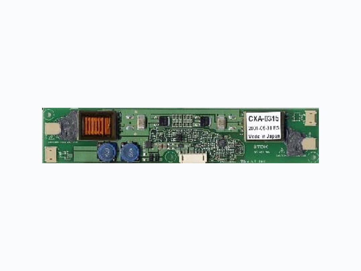
CXA-0315 POWER-SYSTEMS
Document overview
- Manufacturer or author: Provided By www.digicamel.com(FREE DATASHEET DOWNLOAD SITE)
- PDF pages: 2
Technical content
CXA-0315 (21W QUAD OUTPUTS WITH DIMMING FUNCTION) DC-AC INVERTER UNIT Power Systems – The Power Solution Web: www.Power-Systems.de Address: Dörnet 8 ; 74360 Ilsfeld-Auenstein / Germany Email: Info@Power-Systems.de Tel. : + 49 / 70 62 / 67 59 - 6 Fax: + 49 / 70 62 / 67 59 - 80 All specification are subject to change without notice. Page (1 / 2) VER, 16 Juni 2003 DESCRIPTION : This DC to AC Inverter was developed for many other low LCD Backlight power supply as low profile applications, either for LCD Monitor or Industrial PC. APPLIC AB LE LCD : 15 to 17inch quad lamp type Lamp Voltage 700V Lamp Current 7.5mA Lamp Start Up Voltage 1800Vrms FEATURES : PWM dimming type. Current Feedback Circuit High Efficiency Regulated output current TEMPERA TURE & HUMDITY : Operating Temperature Range 0 °C ~ +60°C Storage Temperature Range -30 °C ~ +85°C Humidity 95 %RH max DIMENSIONS : Unit : mm Weight : 44 (g) typ. C XA-0315 060 2 M AD E IN JAPANCN 3 CN5 CN2 CN 4 CN1 T0 1T02 80 ± 0.3 93 ± 0.3 37 ± 0.5 180 ± 0. 5 3.5 ± 0.5 3.5 ± 0.5 28 ± 0.3 3 - Ø3.0 ± 0.2 8.5max High Voltage generation area 60mmHigh Voltage generation area 60mm 4 4 Vlow3 / Vlow4 Vlow1 / Vlow2 Vhigh3 / Vhigh4 Vhigh1 / Vhigh2 0 ~ 5.5V CN1-1 CN1-2 CN1-3 CN1-4 (JST)4 Connector CN4,5 SM02(4.0)B-BHS2 Pin CN1-5 CN1-6 CN1-7 Symbol Vin GND Vrmt Vbr NC Note 0 V CN1 : S7B-PH-SM3 (JST) No. Part Description PWB Connector CN1 Connector CN2,3 Note UL94V-0 t=1.0mm S7B-PH-SM3 SM02B-BHSS-1 Qty. 2 (JST) (JST) CN2,CN4 : SM02B-BHSS-1 (JST) CN2-1 / CN2-2 CN3-1 / CN3-2 Pin Symbol Note 700Vrms (7.5mArms) 700Vrms (7.5mArms) CN3.CN5 : SM02(4.0)B-BHS (JST) CN4-1 / CN4-2 CN5-1 / CN5-2 Pin Symbol Note (2V) (2V)0 ~ 0.4V : OFF 2.5V ~ Vin : ON 10.8 ~ 13.2V
CXA-0315 (21W QUAD OUTPUTS WITH DIMMING FUNCTION) DC-AC INVERTER UNIT Power Systems – The Power Solution Web: www.Power-Systems.de Address: Dörnet 8 ; 74360 Ilsfeld-Auenstein / Germany Email: Info@Power-Systems.de Tel. : + 49 / 70 62 / 67 59 - 6 Fax: + 49 / 70 62 / 67 59 - 80 All specification are subject to change without notice. Page (2 / 2) VER, 16 Juni 2003 RL1 ~ 4 (k )Ω ELECTRICAL CHARACTERISTICS : Output Current Input Current1 Frequency Open Voltage Parameters Symbol Conditions Vin (V) Unit Specifications Iout Iin1 FL Vopen 6.5 7.5 8.5 mArms kHz Vrms typ.min. max. 22 . 5 40 45 50 1700 1800 - TEST CIRCUIT : Adc 345 12 ± 1.2 12 ± 1.2 -1 - mAdcInput Current2 Iin2 Note 2 : Open circuit on all lamps for more than 3 seconds, will shut the inverter down 77 . 5812 ± 1.2 V (V) 5 ± 0.25 5 ± 0.25 5 ± 0.25 5 ± 0.25 5 ± 0.25 0 ± 0.25 5 ± 0.25 0 ~ 60 0 ~ 60 0 ~ 60 0 ~ 60 0 ~ 60 Ta ( )°C 0 ~ 60 23 ± 5 12 ± 1.2 12 ± 1.2 12 ± 1.2 12 ± 1.2 Vbr (V) Duty(High)* 65 ± 0.5% Vbr=0V:Brightness MAX Iin Vopen SW1Vr mt 0/5V CN1-1.2 Vin CN1-3.4 GND CN1-6 NC Q6 T1 8,9 1000: 1 PROBE CN1-7 Vrmt CN1-5 Vbr Vbr 0 / 5V a b C20 C21 CN3-1 V high3 CN5-1 Vlow3CN3-2 V high4 CN5-2 Vlow4 C18 C19 CN4-1 Vlow1 SW2 SW3 RL 1 Iout1 RL 2 Iout2 CN2-1 Vhigh1 CN2-2 Vhigh2 CN4-2 Vlow2 RL 4 Iout4 RL3 Io ut3 SW5 SW4 T2 8,9 V A A V A Vin 10.8~13.2V * High (=5V) 65% , Low (=0V) 35% Freq = 270 Hz Note 1 : Please keep minimum of 2mm clearance (all directions) between inverter high voltage area as marked on mechanical drawing and any conductors. SW1 a b Operation of unit Operation Non operation Non operationOpen Open Close Operation of shutdown Operation Non operation SW2~ SW5