


 Download PDF
CX74038 SKYWORKS
Document overview
- PDF pages: 12
Technical content
Page 1

DATA SHEET
CX74038: 2.6 GHz/800 MHz Dual Fractional-N/lnteger-N
Frequency Synthesizer
Applications
- Multi-slot GSM/DCS
- PCS/W-CDMA
- Portable communication systems
- Dual-mode cellular telephone systems
- Spread spectrum receivers
- Wireless LAN systems
- Wireless routers and WLL systems
- SATCOM receivers
Features
- Maximum operating frequency: 2.6 GHz
- Maximum IF synthesizer frequency: 800 MHz
- Supply voltage as low as 2.6 V
- Fast frequency settling time with fractional-N operation
- Internal fractional spur reduction
- Programmable charge pump currents
- Digital lock detector
- Power saving at lower frequency
- TSSOP (20-pin, 6.5 x 4.4 x 1.0 mm) package
Description
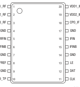
The Skyworks CX74038 is a complete, low-power 2.6 GHz/800 MHz dual frequency synthesizer. The device provides both Radio Frequency (RF) channels and Intermediate Frequency (IF) channels. Fractional-N operation offers low phase noise, fast settling time, and low spurious tones for RF channels. A standard integer-N division is used for IF channels. The three-wire serial interface provides programmable control of the frequency synthesizer to support dual-conversion transceivers. The 20-pin Thin Shrink Small Outline Package (TSSOP) device package and pin configuration are shown in Figure 1. A functional block diagram of the CX74038 is shown in Figure 2.
VDD1_RF
VDD2_RF
CPO_RF
C1452
Figure 1. CX74038 Pinout – 20-Pin TSSOP
(Top View)
Page 2
GND VDD2_RF VDD1_RF GND CPO_RF GND
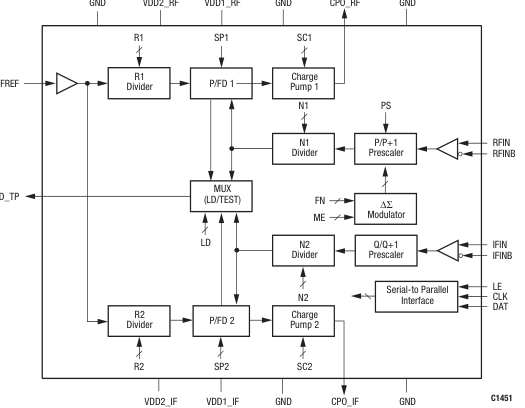
Figure 2. CX74038 Frequency Synthesizer Block Diagram
Technical Description
The CX74038 is a fractional-N frequency synthesizer using a ∆Σ modulation technique. The fractional-N implementation provides low in-band noise by having a low division ratio and fast frequency settling time. In addition, the CX74038 provides arbitrarily fine frequency resolution with digital words, so that the frequency synthesizer can be used to compensate for crystal frequency drift in the RF transceiver.
∆Σ Modulator Fractional spurs are the primary limitation of conventional fractional-N synthesizers. The CX74038 ∆Σ technique improves the synthesizer performance by randomizing the spurs using internal dithering.
Serial Interface The serial interface is a versatile three-wire interface consisting of three pins: the serial clock (CLK), serial input (DAT), and Latch Enable (LE). This interface enables the CX74038 to operate in a system where one or multiple masters and slaves are present. For more information, refer to the Synthesizer Register Programming section of this document.
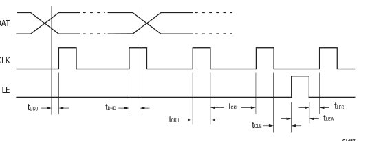
As shown in Figure 3, LE is set low before the rising edge of the first clock (CLK) pulse and is held low until after the last (22nd) clock pulse, at which time LE is set high. The data word is transferred to the correct device register when LE is high (there are four internal registers selected by the D1 and D0 bits of the 22-bit data/address word. See Figure 4). If the LE signal does not go high, the data does not get transferred to the register. Between each 22-bit data/address word transfer, LE must be pulsed to make the transfer to the specific device register. Data/address transfer is MSB first. LE must not go high when CLK is high; otherwise, the data word
is not transferred to the register. LE must only go high after CLK has gone low. After the transfer of the last 22-bit data/address word, the LE signal can be left in a high state. It does not have to be returned to a low state unless another data/address word transfer is required. It is not necessary to write all four data/address words to the synthesizer to make a change in programming. For example, if a change to the Lock Detect (LD) pin operation is desired, only word 00 has to be changed.
Page 3
C1457
Figure 3. CX74038 Serial Data Input Timing Diagram (MSB First)
MSB
LSB

C1456
Figure 4. CX74038 Serial Data Word Format
Registers The CX74038 includes four 22-bit registers that can be programmed independently in any order. Bits D0 and D1 represent the register addresses. For more information on registers, addresses, and format, refer to the Synthesizer Register Programming section of this document. A dithering disable function is accessible via word 00, data bits 21 and 20. When the RF synthesizer is programmed for fractional divide values, these bits should be programmed to 1 0 (dithering enable). However, when the RF synthesizer is programmed to output a frequency which is a whole integer multiple of the comparison frequency, the synthesizer should be programmed for dithering disabled (bits set to 11). This improves the phase noise
when operating on integer-N boundaries. These data bits must be programmed after power-up, otherwise erroneous device operation may occur. Refer to the Synthesizer Register Programming section of this document for bit definitions.
Voltage Controlled Oscillator (VCO) Prescalers The VCO prescalers, P/P+1 and Q/Q+1, provide low noise signal conditioning of the VCO signals. They translate from an off-chip, single-ended or differential signal to an on-chip differential signal. By changing the PS bit, the RF synthesizer has the option to use either the 8/9 or the 16/17 prescaler depending on the desired
operational frequency. The maximum frequency is 2.6 GHz for the 16/17 prescaler and 1.4 GHz for the 8/9 prescaler. The IF synthesizer has a fixed 16/17 prescaler with a maximum frequency of 800 MHz.
RF and IF Dividers The CX74038 provides programmable dividers that control the prescaler and supply the divided VCO signals to the charge pump phase detectors. Programmable ratios on the RF fractional-N synthesizer ranging from 256 to 212 are possible with the 16/17 prescaler, and from 64 to 211 with the 8/9 prescaler. The IF integer-N synthesizer has a programmable divide ratio ranging from 256 to 217.
Reference Frequency Dividers The reference signal can be divided by a ratio of 1 to 7 for the RF reference divider (R1) and from 1 to 8192 for the IF reference divider (R2). The input frequency for the reference signal can be as high as 50 MHz.
Phase Detectors and Charge Pumps The CX74038 uses a separate charge pump phase detector for each synthesizer. The IF and RF Phase/Frequency Detector (PFD)
Page 4
can have a programmable charge pump current from 0.4 mA to 1.6 mA and 120 µA to 480 µA, respectively. For optimum performance, the divided reference frequency presented at the phase detector input must not exceed 9 MHz using the RF 16/17 prescaler synthesizer mode, 15 MHz using the RF 8/9 prescaler, or 2 MHz for the IF synthesizer mode. The comparison frequency is also limited by the desired frequency divided by the minimum divide ratio. The charge-pump can be programmed to high impedance (Hi-Z) state for open-loop VCO modulation use.
Lock Detection The output of the IF/RF dividers (R1, N1, R2, N2) and lock detectors for both synthesizers can be multiplexed to the LD pin. When programmed for lock detection, the CX74038 provides an active low output to indicate the out-of-lock condition. When locked, the LD pin is high.
Power Down The CX74038 supports a number of power-down modes through the serial interface. Both IF and RF synthesizer blocks can be powered down, powered up individually, or both powered up using the EN bits (see the Synthesizer Register Programming section of this document). The CX74038 is enabled at power up by default.
Synthesizer Register Programming IF Integer-N Synthesizer. The N2 17-bit divider ratio is calculated using the following equation:
FREF IF = N2 -------------
R2
As with all integer-N synthesizers, the minimum step size is related to the divided reference frequency, FREF. RF Fractional-N Synthesizer. The N1 divider ratio is calculated using the following equation:
FREF RF = ------------- N1Total R1
where: N1Total = N1 + 3.5 + FN + ME
FN sets the fractional-N modulo up to 256 modulo, as calculated by:
1 1 1
1
----- -----
-----
2-- FN = + + + ... + D2
D9 D8
D7 22 23
28
where: Dn represents the bit locations within the register field. The fractional modulo can be extended up to 221 using the modulo extender (ME), if required, as shown by the following equation:
1 1 1
1
ME = ----- + ------- + ------- + ... + --------
D21 D20 D19
D9
29 210 211
221
Because the way the ∆Σ modulator is implemented in the CX74038, the number 3.5 must be added to the division number to obtain the final division ratio. If the integer field of the N divider shows a non-integer number, the desired frequency or the division fraction portion needs to be adjusted. Sample calculations for two fractional-N applications are shown in Figure 5.
Electrical and Mechanical Specifications
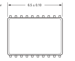
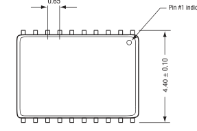
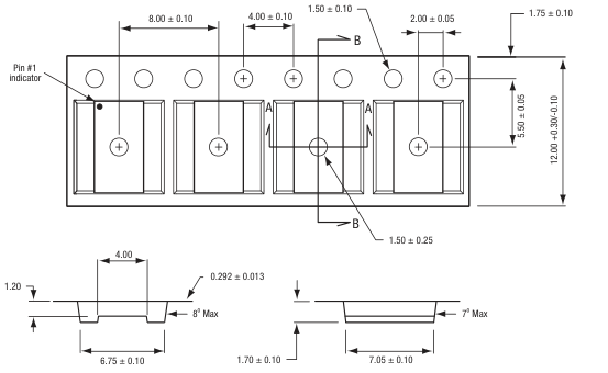
Signal pin assignments and functional pin descriptions are specified in Table 1. The absolute maximum ratings of the CX74038 are provided in Table 2. The recommended operating conditions are specified in Table 3 and electrical characteristics are provided in Table 4. Table 5 provides the register descriptions. Package dimensions for the CX74038 are shown in Figure 6 and tape and reel dimensions for the 20-pin TSSOP package are shown in Figure 7.
Electrostatic Discharge Information
The CX74038 is an electrostatic sensitive device. Observe precautions when handling.
Page 5
Case 1: To achieve a desired FVCO_RF frequency of 2440.2 MHz using a crystal frequency of 24 MHz with operation of the synthesizer in RF mode using the 16/17 prescaler (PS = 1). R1 is set to divide by 3 to achieve a comparison frequency of 8 MHz, since the maximum internal reference frequency is 9 MHz. Divide the operating frequency by the internal reference frequency to determine the value of NTotal:
NTotal = 2440.2 MHz 8 MHz
= 305.025
Subtract 3.5 from NTotal and remove the fractional portion of the result to determine N1:
305.025 – 3.5 = 301.525
N1 = 301 (decimal)
Fractional portion = 0.525 (decimal)
N1 = 000100101101 (binary) D21 -----------D10 Register Address 112
Multiply the fractional portion of N1 by 256 and remove the fractional portion of the result to determine FN:
0.525 × 256 = 134.4
FN = 134 (decimal)
FN = 10000110 (binary) D9 -------D2 Register Address 112
Divide FN by 256 to determine the actual fractional portion:
134 = 0.5234375 256
Subtract this result from the fractional portion of N1:
0.525 – 0.5234375 = 0.0015625
Multiply this result by 2097152 (the 21-bit ∆Σ modulator value 221) and remove the fractional portion to determine the ME:
0.0015625 × 2097152 = 3276.8
ME = 3276 (decimal)
ME = 0110011001100 (binary) D21 --------------D9 Register Address 012
In this example, N1 is greater than 256, the minimum divide ratio for the 16/17 prescaler.
C1454
Figure 5. Fractional-N Applications: Sample Calculation (1 of 2)
Page 6
Case 2: To achieve a desired FVCO_RF frequency of 1400 MHz using a crystal frequency of 13 MHz with operation of the synthesizer in RF mode using the 8/9 prescaler (PS = 0). The crystal frequency does not need to be divided further, since the maximum comparison frequency is 15 MHz. Divide the operating frequency by the internal reference frequency to determine the value of NTotal:
NTotal = 1400 MHz 13 MHz
=107.6923076
Subtract 3.5 from NTotal and remove the fractional portion of the result to determine N1:
107.6923076 – 3.5 = 104.1923076
N1 = 104 (decimal)
Fractional portion = 0.1923076 (decimal)
N1 = 000001101000 (binary) D21 ------------D10 Register Address 112
Multiply the fractional portion of N1 by 256 and remove the fractional portion of the result to determine FN:
0.1923076 × 256 = 49.230746
FN = 49 (decimal)
FN = 00110001 (binary) D9 -------D2 Register Address 112
Divide FN by 256 to determine the actual fractional portion:
49 = 0.1914962 256
Subtract this result from the fractional portion of N1:
0.1923076 – 0.1914062 = 0.0009014
Multiply this result by 2097152 (the 21-bit ∆Σ modulator value 221) and remove the fractional portion to determine the ME:
0.0009014 × 2097152 = 1890.3728
ME = 1890 (decimal)
ME = 0011101100010 (binary) D21 --------------D9 Register Address 012
In this example, N1 is greater than 64, the minimum divide ratio for the 8/9 prescaler.
C1455
Figure 5. Fractional-N Applications: Sample Calculation (2 of 2)
Page 7
Table 1. CX74038 Signal Descriptions
| Pin # | Pin Name | I/O | Description | Pin # | Pin Name | I/O | Description |
|---|---|---|---|---|---|---|---|
| 1 | VDD1_RF | — | Power supply for RF digital circuits | 11 | CLK | I | Serial interface clock input |
| 2 | VDD2_RF | — | Power supply for RF analog circuits | 12 | DAT | I | Serial interface data input |
| 3 | CPO_RF | O | RF charge pump output | 13 | LE | I | Serial interface Latch Enable input |
| 4 | GND | — | Ground | 14 | GND | — | Ground |
| 5 | RFIN | I | RF prescaler input | 15 | IFINB | I | IF prescaler complementary input |
| 6 | RFINB | I | RF prescaler complementary input | 16 | IFIN | I | IF prescaler input |
| 7 | GND | — | Ground | 17 | GND | — | Ground |
| 8 | FREF | I | Reference divider input | 18 | CPO_IF | O | IF charge pump output |
| 9 | GND | — | Ground | 19 | VDD2_IF | — | Power supply for IF analog circuits |
| 10 | LD_TP | O | Multiplexed output from lock detectors and dividers | 20 | VDD1_IF | — | Power supply for IF digital circuits |
Table 2. Absolute Maximum Ratings
| Parameter | Minimum | Maximum | Units |
|---|---|---|---|
| Power supply with GND = 0 V | –0.3 | +3.6 | V |
| Voltage on any pin | GND | V | |
| Storage temperature | –65 | +150 | °C |
Note: Exposure to maximum rating conditions for extended periods may reduce device reliability. There is no damage to device with only one parameter set at the limit and all other parameters set at or below their nominal values.
Table 3. Recommended Operating Conditions
| Parameter | Min | Max | Units |
|---|---|---|---|
| Power supply | 2.6 | 3.6 | V |
| Operating junction temperature | –40 | +100 | °C |
| Operating ambient temperature | –40 | +85 | °C |
Page 8
Table 4. Electrical Characteristics (VDD = 2.7 V, TA = 25 °C, unless otherwise noted)
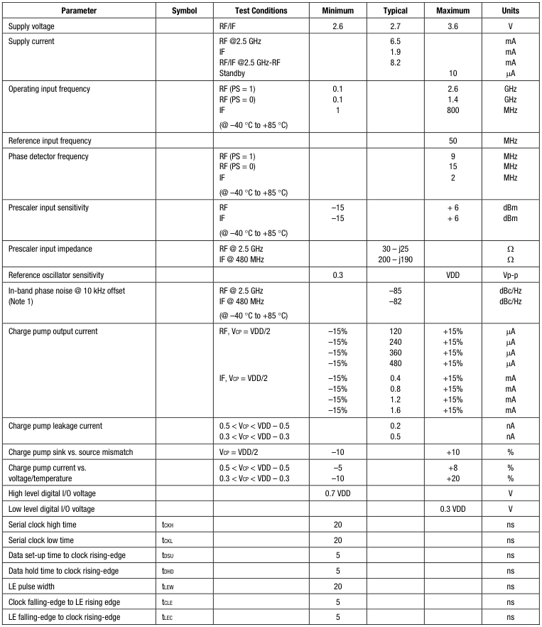
Note 1: RF output frequency = 2.5 GHz, comparison frequency = 8 MHz, loop bandwidth = 35 kHz, and charge pump current = 480 mA. IF output frequency = 480 MHz, comparison frequency = 200 kHz, loop bandwidth = 10 kHz, and charge pump current = 1.6 mA.
Page 9
Table 5. CX74038 Register Descriptions (1 of 2)
| Symbol | Function | Description |
|---|---|---|
| Register Word Address 00 | ||
| Address bits [1:0] | 00 | |
| SC2 | IF synthesizer charge-pump output current [3:2] | Bits [3:2] select the IF synthesizer charge pump output current: bit 3 bit 2 0 0 Selects 0.4 mA charge pump output current 0 1 Selects 0.8 mA charge pump output current 1 0 Selects 1.2 mA charge pump output current 1 1 Selects 1.6 mA charge pump output current |
| LD | Test mode [6:4] | Bits [6:4] set the test mode: bit 6 bit 5 bit 4 0 0 0 multiplexes Ndiv output of IF SX to LD output 0 0 1 multiplexes Rdiv output of IF SX to LD output 0 1 0 multiplexes lock detect output of IF SX to LD output 0 1 1 multiplexes ANDed lock detect of both SX to LD output 1 0 0 multiplexes Ndiv output of RF SX to LD output 1 0 1 multiplexes Rdiv output of RF SX to LD output 1 1 0 multiplexes lock detect output of RF SX to LD output 1 1 1 Hi-Zs the charge-pump output of RF SX |
| R2 | IF synthesizer reference divider [19:7] | Bits [19:7] set the IF synthesizer 13-bit reference divider ratio |
| RF synthesizer fractional-N mode selection [21:20] (Note 1) | Bits [21:20] set the RF synthesizer fractional-N mode: bit 21 bit 20 0 0 Reserved 0 1 Reserved 1 0 Fractional-N mode with dithering 1 1 Fractional-N mode without dithering | |
| Register Word Address 01 | ||
| Address bits [1:0] | 01 | |
| SP1 | RF synthesizer phase detector output polarity [2] | Bit [2] sets the polarity of the RF synthesizer phase detector output: 0 Sets phase detector output for negative VCO gain 1 Sets phase detector output for positive VCO gain |
| SC1 | RF synthesizer charge-pump output current [4:3] | Bits [4:3] set the RF synthesizer charge pump output current: bit 4 bit 3 0 0 Selects 120 µA charge pump output current 0 1 Selects 240 µA charge pump output current 1 0 Selects 360 µA charge pump output current 1 1 Selects 480 µA charge pump output current |
| PS | RF synthesizer prescaler selection [5] | Bit [5] selects the RF synthesizer prescaler: 0 Select 8/9 prescaler 1 Select 16/17 prescaler |
| R1 | RF synthesizer reference divider [8:6] | Bits [8:6] set the RF synthesizer’s 3-bit reference divider ratio |
| ME | RF synthesizer modulo extender [21:9] | Bits [21:9] extend the RF synthesizer’s fractional modulo up to 2,097,152 (optional) |
Page 10
Table 5. CX74038 Register Descriptions (2 of 2)
| Symbol | Function | Description |
|---|---|---|
| Register Word Address 10 | ||
| Address bits [1:0] | 10 | |
| SP2 | IF synthesizer phase detector output polarity [2] | Bit [2] sets the IF synthesizer phase detector output: 0 Sets phase detector output for negative VCO gain 1 Sets phase detector output for positive VCO gain |
| EN | Enable mode [4:3] | Bits [4:3] enable the RF and/or IF synthesizers: bit 4 bit 3 0 0 Enables both RF SX and IF SX 0 1 Enables only RF SX 1 0 Enables only IF SX 1 1 Sets power-down mode for both RF/IF SX |
| N2 | IF synthesizer main divider [21:5] | Bits [21:5] set the IF synthesizer 17-bit main divider ratio |
| Register Word Address 11 | ||
| Address bits [1:0] | 11 | |
| FN | RF synthesizer fractional-N division [9:2] | Bits [9:2] set the RF synthesizer’s fractional-N program up to 256 modulo |
| N1 | RF synthesizer main divider [21:10] | Bits [21:10] set the RF synthesizer’s 12-bit main divider ratio with a 16/17 prescaler, or an 11-bit main divider ratio with 8/9 prescaler |
Note 1: These bits must be programmed after power is applied to the device. Failure to do so may result in erroneous device operation.
Page 11
0.65
Top View
Bottom View
1.00 +0.05/–0.20

1.00 Ref
Side View
End View
All measurements are in millimeters
C003
Figure 6. CX74038 20-Pin TSSOP Package Dimensions
A
B
Notes: 1. Carrier tape material: black conductive polystyrene 2. Cover tape material: transparent conductive PSA 3. Cover tape size: 9.3 mm width
C879
- All measurements are in millimeters
Figure 7. CX74038 20-Pin TSSOP Tape and Reel Dimensions
Page 12
Ordering Information
| Model Name | Manufacturing Part Number | Evaluation Kit Part Number |
|---|---|---|
| CX74038 2.6 GHz/800 MHz Frequency Synthesizer | CX74038-12 | PH00-D222 |
Copyright © 2002, 2003, 2004, 2005 Skyworks Solutions, Inc. All Rights Reserved.
Information in this document is provided in connection with Skyworks Solutions, Inc. (“Skyworks”) products. These materials are provided by Skyworks as a service to its customers and may be used for informational purposes only by the customer. Skyworks assumes no responsibility for errors or omissions in these materials. Skyworks may make changes to its documentation, products, specifications and product descriptions at any time, without notice. Skyworks makes no commitment to update the information and shall have no responsibility whatsoever for conflicts, incompatibilities, or other difficulties arising from future changes to its documentation, products, specifications and product descriptions.
No license, express or implied, by estoppel or otherwise, to any intellectual property rights is granted by or under this document. Except as may be provided in Skyworks’ Terms and Conditions of Sale for such products, Skyworks assumes no liability whatsoever in association with its documentation, products, specifications and product descriptions.
THESE MATERIALS ARE PROVIDED “AS IS” WITHOUT WARRANTY OF ANY KIND, EITHER EXPRESS OR IMPLIED OR OTHERWISE, RELATING TO SALE AND/OR USE OF SKYWORKS PRODUCTS INCLUDING WARRANTIES RELATING TO FITNESS FOR A PARTICULAR PURPOSE, MERCHANTABILITY, PERFORMANCE, QUALITY OR NON-INFRINGEMENT OF ANY PATENT, COPYRIGHT OR OTHER INTELLECTUAL PROPERTY RIGHT. SKYWORKS FURTHER DOES NOT WARRANT THE ACCURACY OR COMPLETENESS OF THE INFORMATION, TEXT, GRAPHICS OR OTHER ITEMS CONTAINED WITHIN THESE MATERIALS. SKYWORKS SHALL NOT BE LIABLE FOR ANY DAMAGES, INCLUDING SPECIAL, INDIRECT, INCIDENTAL, OR CONSEQUENTIAL DAMAGES, INCLUDING WITHOUT LIMITATION, LOST REVENUES OR LOST PROFITS THAT MAY RESULT FROM THE USE OF THESE MATERIALS WHETHER OR NOT THE RECIPIENT OF MATERIALS HAS BEEN ADVISED OF THE POSSIBILITY OF SUCH
DAMAGE.
Skyworks products are not intended for use in medical, lifesaving or life-sustaining applications. Skyworks’ customers using or selling Skyworks products for use in such applications do so at their own risk and agree to fully indemnify Skyworks for any damages resulting from such improper use or sale.
The following are trademarks of Skyworks Solutions, Inc.: Skyworks®, the Skyworks logo, and Breakthrough Simplicity®. Product names or services listed in this publication are for identification purposes only, and may be trademarks of Skyworks or other third parties. Third-party brands and names are the property of their respective owners. Additional information, posted at www.skyworksinc.com, is incorporated by reference.