


 Download PDF
CX74005 SKYWORKS
Document overview
- PDF pages: 14
Technical content
Page 1

VGA + I/Q Demodulator Rx ASIC for Portable Phone Applications
The CX74005 Application-Specific Integrated Circuit (ASIC) is a Variable Gain Amplifier (VGA) and I/Q demodulator, intended for use in Code Division Multiple Access (CDMA) portable phones in both cellular and Personal Communications System (PCS) bands. As a trimode IC, it can be used in CDMA mode or Advanced Mobile Phone System (AMPS) mode.
The device incorporates a VGA and the In-Phase and Quadrature (I/Q) demodulator stages. The intermediate frequencies (IF) are combined through separate buffers at the input of the VGA depending on the selected mode. The VGA has a gain control range greater than 90 dB.
There are two Very High Frequency (VHF) oscillators that operate with external tank circuits. They provide signals to the Local Oscillator (LO) for the I/Q demodulator in the cellular and PCS bands.
The noise figure, gain, and third order Input Intercept Point (IIP3) of the CX74005 are optimized to meet the system requirements for AMPS and CDMA modes as per TIA/EIA-98-B, ANSI J-STD-018 (PCS), CDMA2000. Employing silicon bipolar technology, the ASIC is designed for high performance, a high level of integration and low cost.
The device package and pinout are shown in Figure 1. A block diagram of the CX74005 is shown in Figure 2.
Features
- Supports CDMA/AMPS/PCS1900 modes
- Three battery cell operation (2.7 V < VCC < 3.3 V).
- IF inputs and I/Q outputs
- On-chip 100 to 640 MHz oscillators
- Low power operation: <25 mA
- 32-pin Land Grid Array (LGA) 5 x 5 mm package
Applications
- Tri-mode handsets
- CDMA and AMPS modes in the cellular band: − AMPS − CDMA-US − CDMA-Japan
- CDMA mode in the PCS band: − PCS-US − PCS-Korea
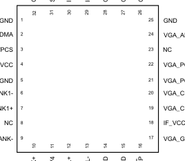
FM/CDMA
VGA_AMPS
CELL/PCS
VCO_VCC
VGA_PCS_IN+
VCO_GND
VGA_PCS_IN-
CELL_TANK1-
VGA_CDMA_IN+
CELL_TANK1+
VGA_CDMA_IN-
PCS_TANK-
CNXT044
Figure 1. Rx ASIC Pinout – 32-Pin LGA Package
(Top View)
Data Sheet
Doc. No. 101252A
Page 2
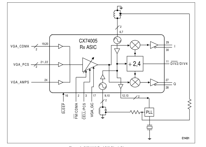
Figure 2. CX74005 Rx ASIC Block Diagram
Technical Description
Variable Gain Amplifier (VGA). The high dynamic range required by CDMA handsets is achieved by the VGA, which is common to all modes. The VGA has a minimum dynamic range of 90 dB with a control voltage of 0.5 to 2.5 volts. The appropriate signal path is switched internal to the device. This eliminates off-chip switching needed to operate this common VGA in cellular AMPS, CDMA, and PCS modes.
I/Q Demodulator. The local oscillator signals are generated on- chip. The I/Q demodulator is internally connected to the VGA output. It is designed to have a very low amplitude and phase imbalance. The I and Q outputs are differential. The DC offsets between the differential outputs and between I and Q channels are designed to be extremely low to facilitate compatibility with baseband interfaces.
VHF Oscillators. There are two on-chip oscillators, one for the cellular and one for the PCS bands. These Voltage Controlled Oscillators (VCOs) work with external tank circuits and varactor diodes. The outputs of the differential oscillators are buffered and the output is used to drive the prescaler of an external Phase Locked Loop (PLL). The VCOs typically operate at twice the IF frequency and can operate at up to four times the IF frequency.
The local oscillators for the I/Q demodulators are derived by an on-chip frequency divider. The logic signal to select the divider
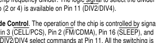
done internally. The supply voltage should be present at all the VCC pins for normal operation. The signals needed to select each mode is shown in Table 1.
Electrical and Mechanical Specifications
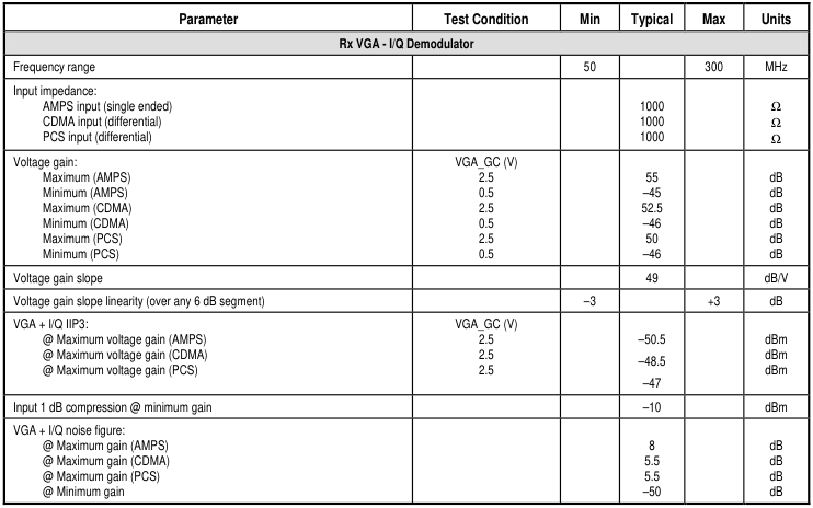
Signal pin assignments and functional pin descriptions are described in Table 2. The absolute maximum ratings of the CX74005 are provided in Table 3. The recommended operating conditions are specified in Table 4. Electrical specifications are provided in Table 5.
Typical performance characteristics are illustrated in Figures 3 through 32. Figure 33 provides the package dimensions for the 32-pin LGA and tape and reel dimensions are shown in Figure 34.
Page 3
ESD Sensitivity
The CX74005 is a Class 1 device. The following extreme Electrostatic Discharge (ESD) precautions are required according to the Human Body Model (HBM):
- Protective outer garments.
- Handle device in ESD safeguarded work area.
- Transport device in ESD shielded containers.
- Monitor and test all ESD protection equipment. The HBM ESD withstand threshold value, with respect to ground, is ±1.5 kV. The HBM ESD withstand threshold value, with respect to VDD (the positive power supply terminal) is also ±1.5 kV.
Table 1. Mode Control Select Signal Switching
| Pin | AMPS | CDMA | PCS |
| 3 (CELL/PCS) | 0 | 0 | 1 |
| 2 (FM/CDMA) | 0 | 1 | x |
| 16 (SLEEP) | 1 | 1 | 1 |
| Key: 0 = Low 1 = High x = N/A Note: DIV 2 is used in the evaluation board. | |||
Page 4
Table 2. CX74005 Pin Assignments and Signal Descriptions
| Pin # | Name | Description |
|---|---|---|
| 1 | GND | Ground |
| 2 | FM/CDMA | Cellular band mode select: 0 = AMPS, 1 = CDMA |
| 3 | CELL/PCS | Band select: 0 = Cellular; 1 = PCS |
| 4 | VCO_VCC | Voltage supply pin to the VCO buffers. A bypass capacitor should be placed close to the device from pin 4 to pin 5. The trace should be short and connected immediately to the ground plane for best performance. |
| 5 | VCO_GND | Ground return from the VCO buffers. |
| 6 | CELL_TANK1– | Differential tank connection for the cellular band VCO. Care should be taken during the layout of the external tank circuit to prevent parasitic oscillations. |
| 7 | CELL_TANK_1+ | Differential tank connection for the cellular band VCO. Care should be taken during the layout of the external tank circuit to prevent parasitic oscillations. |
| 8 | NC | No connection |
| 9 | PCS_TANK– | Differential tank connection for the PCS band VCO. Care should be taken during the layout of the external tank circuit to prevent parasitic oscillations. |
| 10 | PCS_TANK+ | Differential tank connection for the PCS band VCO. Care should be taken during the layout of the external tank circuit to prevent parasitic oscillations. |
| 11 | DIV2/DIV4 | Selects the divide ratio of the VCO to the LO port of the I/Q demodulator: 0 = divide by 2, 1 = divide by 4. |
| 12 | PLL+ | Differential buffered VCO output |
| 13 | PLL– | Differential buffered VCO output |
| 14 | GND | Ground |
| 15 | IF_GND | Ground |
| 16 | SLEEP | Activates sleep mode: 0 = Sleep, 1 = Enable |
| 17 | VGA_GC | The VGA gain control signal. A DC control voltage should be applied to this pin to vary the gain of the VGA. |
| 18 | IF_VCC | Voltage supply to VGA and I/Q demodulator stages. Supply should be well regulated and bypassed to prevent modulation of the signal by the supply ripple. |
| 19 | VGA_CDMA_IN– | CDMA differential VGA input |
| 20 | VGA_CDMA_IN+ | CDMA differential VGA input |
| 21 | VGA_PCS_IN- | PCS differential VGA input. |
| 22 | VGA_PCS_IN+ | PCS differential VGA input. |
| 23 | GND | Ground |
| 24 | VGA_AMPS | AMPS VGA input |
| 25 | GND | Ground |
| 26 | GND | Ground |
| 27 | Q– | Q channel differential output |
| 28 | Q+ | Q channel differential output |
| 29 | I– | I channel differential output |
| 30 | I+ | I channel differential output |
| 31 | GND | Ground |
| 32 | GND | Ground |
Page 5
Table 3. Absolute Maximum Ratings
| Parameter | Minimum | Maximum | Units |
|---|---|---|---|
| Supply voltage (VCC) | –0.3 | +5.5 | V |
| Input voltage range | –0.3 | VCC | V |
| Power dissipation | 600 | mW | |
| Ambient operating temperature | –30 | +80 | °C |
| Storage temperature | –40 | +125 | °C |
Table 4. Recommended Operating Conditions
| Parameter | Minimum | Typical | Maximum | Units |
|---|---|---|---|---|
| Supply voltage (VCC) | 2.7 | 3.0 | 3.3 | V |
| Operating temperature | –30 | +25 | +80 | °C |
| Impedance of logic inputs | 50 | kΩ | ||
| Logic 0 | 0.0 | 0.5 | V | |
| Logic 1 | VCC – 0.5 | VCC | V |
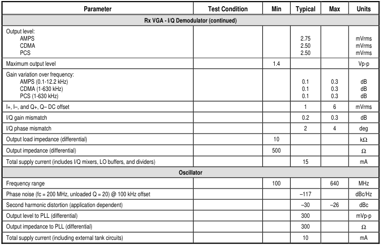
Table 5. CX74005 Rx ASIC Electrical Specifications (1 of 2)
(TA = 25°°°° C, VCC = 3.0 V)
Page 6
Table 5. CX74005 Rx ASIC Electrical Specifications (2 of 2)
(TA = 25°°°° C, VCC = 3.0 V)
Page 7
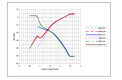
Figure 3. AMPS IIP3 and OIP3 vs. Control Voltage @ 25 C
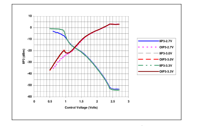
Figure 5. AMPS IIP3 and OIP3 @ –30 ˚C
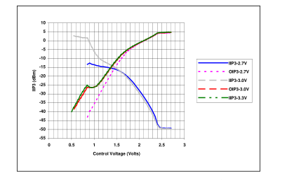
Figure 7. AMPS IIP3 and OIP3 vs. Control Voltage @ 85 C
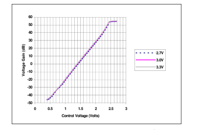
Figure 4. AMPS VGA vs. Control Voltage @ 25 ˚C
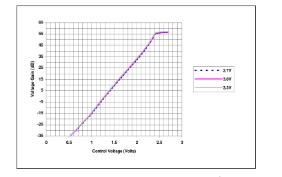
Figure 6. AMPS VGA vs. Control Voltage @ –30 ˚C
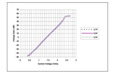
Figure 8. AMPS VGA vs. Control Voltage @ 85 °C
Page 8
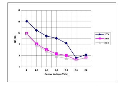
Figure 9. AMPS Noise Figure vs. Control Voltage @ 25 °C
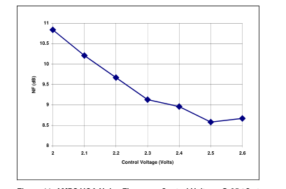
Figure 11. AMPS VGA Noise Figure vs. Control Voltage @ 85 °C at
VCC=3 Volts
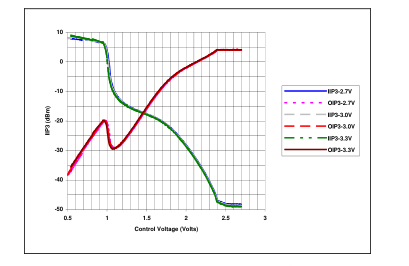
Figure 13. CDMA IIP3 vs. Control Voltage @ 25 °C
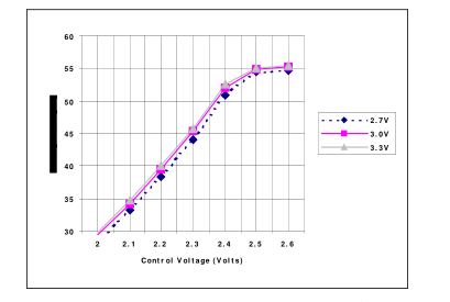
Figure 10. AMPS Gain Noise Figure vs. Control Voltage @ 25 °C
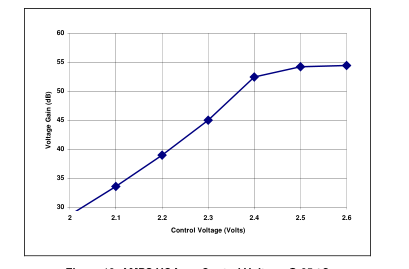
Figure 12. AMPS VGA vs. Control Voltage @ 85 °C
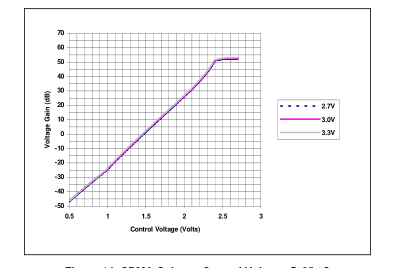
Figure 14. CDMA Gain vs. Control Voltage @ 25 °C
Page 9
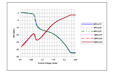
Figure 15. CDMA IIP3 and OIP3 vs. Control Voltage @ –30 °C
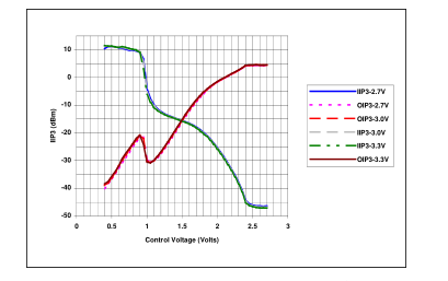
Figure 17. CDMA IIP3 and OIP3 vs. Control Voltage @ 85 °C
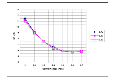
Figure 19. CDMA Noise Figure vs. Control Voltage @ 25 °C
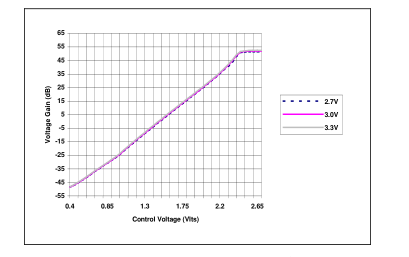
Figure 16. CDMA VGA vs. Control Voltage @ –30 °C
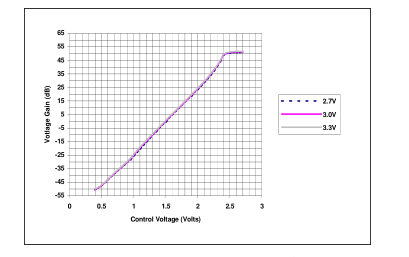
Figure 18. CDMA VGA vs. Control Voltage @ 85 °C
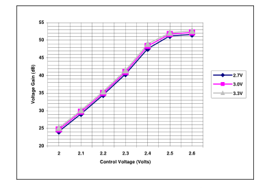
Figure 20. CDMA VGA vs. Control Voltage @ 25 °C
Page 10
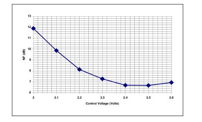
Figure 21. CDMA VGA Noise Figure vs. Control Voltage @ 85 °C
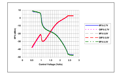
Figure 23. PCS IIP3 and OIP3 vs. Control Voltage @ 25 °C7
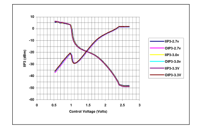
Figure 25. PCS IIP3 vs. Control Voltage @ –30 °C
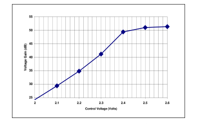
Figure 22. CDMA VGA vs. Control Voltage @ 85 °C
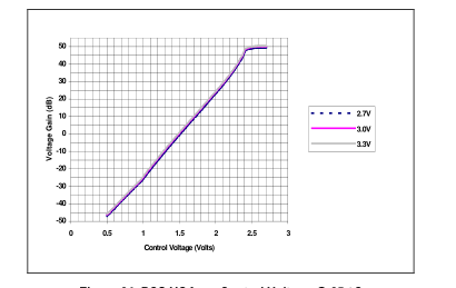
Figure 24. PCS VGA vs. Control Voltage @ 25 °C
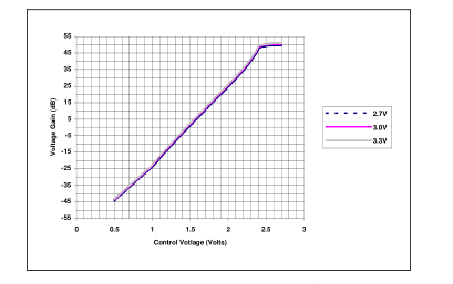
Figure 26. PCS VGA vs. Control Voltage @ –30 °C
Page 11
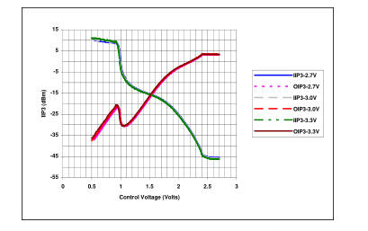
Figure 27. PCS IIP3 and OIP3 vs. Control Voltage @ 85 °C
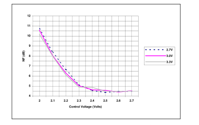
Figure 29. PCS Noise Figure vs. Control Voltage @ 25 °C
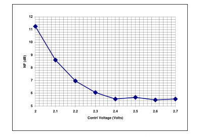
Figure 31. PCS VGA vs. Control Voltage @ 85 °C
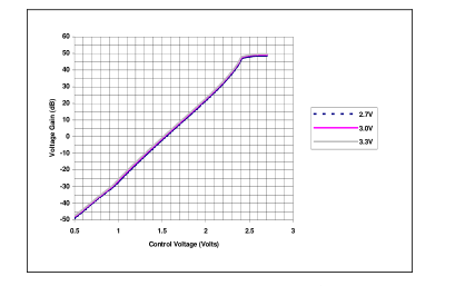
Figure 28. PCS VGA vs. Control Voltage @ 85 °C
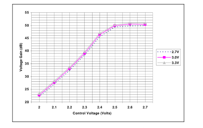
Figure 30. PCS VGA vs. Control Voltage @ 25 °C
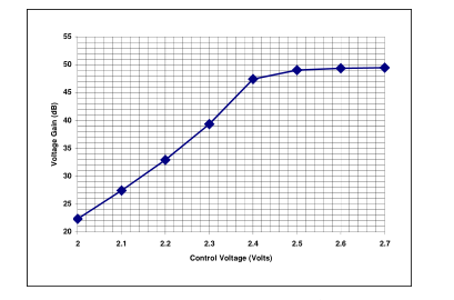
Figure 32. PCS VGA vs. Control Voltage @ 85 °C
Page 12
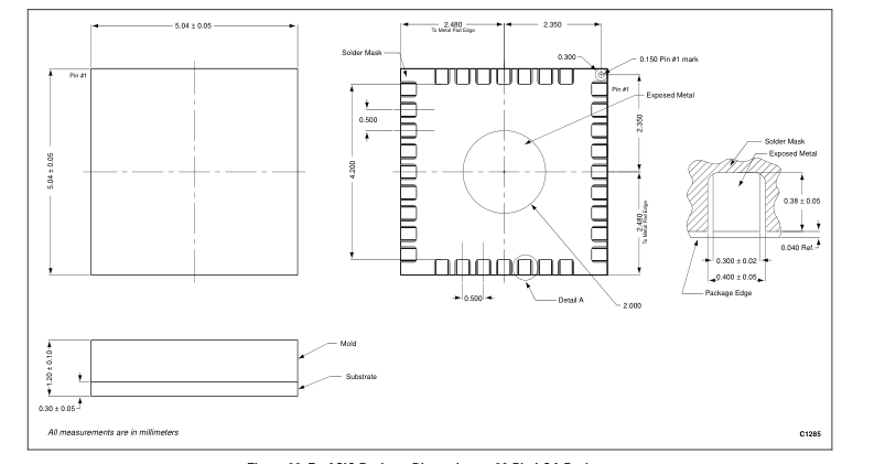
Figure 33. Rx ASIC Package Dimensions – 32-Pin LGA Package
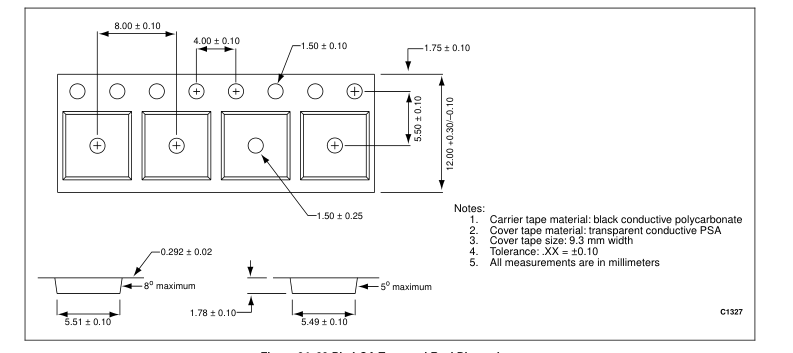
Figure 34. 32-Pin LGA Tape and Reel Dimensions
Page 13
Ordering Information
| Model Name | Manufacturing Part Number | Product Revision |
|---|---|---|
| Rx ASIC | CX74005 |
© 2001, 2002, Skyworks Solutions, Inc. All Rights Reserved. Information in this document is provided in connection with Skyworks Solutions, Inc. ("Skyworks") products. These materials are provided by Skyworks as a service to its customers and may be used for informational purposes only. Skyworks assumes no responsibility for errors or omissions in these materials. Skyworks may make changes to its products, specifications and product descriptions at any time, without notice. Skyworks makes no commitment to update the information and shall have no responsibility whatsoever for conflicts, incompatibilities, or other difficulties arising from future changes to its products and product descriptions.
No license, express or implied, by estoppel or otherwise, to any intellectual property rights is granted by this document. Except as may be provided in Skyworks’ Terms and Conditions of Sale for such products, Skyworks assumes no liability whatsoever. THESE MATERIALS ARE PROVIDED "AS IS" WITHOUT WARRANTY OF ANY KIND, EITHER EXPRESS OR IMPLIED, RELATING TO SALE AND/OR USE OF SKYWORKS™ PRODUCTS INCLUDING WARRANTIES RELATING TO FITNESS FOR A PARTICULAR PURPOSE, MERCHANTABILITY, PERFORMANCE, QUALITY OR NON-INFRINGEMENT OF ANY PATENT, COPYRIGHT OR OTHER INTELLECTUAL PROPERTY RIGHT. SKYWORKS FURTHER DOES NOT WARRANT THE ACCURACY OR COMPLETENESS OF THE INFORMATION, TEXT, GRAPHICS OR OTHER ITEMS CONTAINED WITHIN THESE MATERIALS. SKYWORKS SHALL
NOT BE LIABLE FOR ANY SPECIAL, INDIRECT, INCIDENTAL, OR CONSEQUENTIAL DAMAGES, INCLUDING WITHOUT LIMITATION, LOST REVENUES OR LOST PROFITS THAT MAY RESULT FROM THE USE OF THESE MATERIALS. Skyworks™ products are not intended for use in medical, lifesaving or life-sustaining applications. Skyworks’ customers using or selling Skyworks™ products for use in such applications do so at their own risk and agree to fully indemnify Skyworks for any damages resulting from such improper use or sale. The following are trademarks of Skyworks Solutions, Inc.: Skyworks™, the Skyworks symbol, and “Breakthrough Simplicity”™. Product names or services listed in this
publication are for identification purposes only, and may be trademarks of third parties. Third-party brands and names are the property of their respective owners. Additional information, posted at www.skyworksinc.com, is incorporated by reference.
Page 14

General Information: Skyworks Solutions, Inc. 4311 Jamboree Rd. Newport Beach, CA 92660-3007 www.skyworksinc.com