
CT416 ALLEGRO
Document overview
- Manufacturer or author: Provided By www.digicamel.com(free datasheet download site)
- PDF pages: 33
Technical content
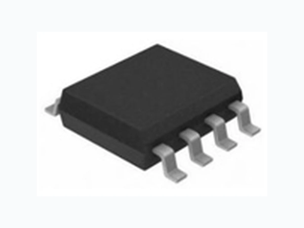
The CT416 is a high bandwidth and ultra-low noise integrated contact current sensor that uses Allegro patented XtremeSense™ TMR technology to enable high accuracy current measurements for many consumer, enterprise, and industrial applications. The device supports eight current ranges where the integrated current carrying conductor (CCC) will handle up to 65 A of current and generates a current measurement as a linear analog output voltage. The device achieves a total output error of about ±1.0% full-scale (FS). The device has a ~300 ns output response time while the current consumption is about 6.0 mA and is immune to common-mode fields. The CT416 has a filter function to reduce the noise on the output pin. The CT416 is offered in an industry-standard 8-lead SOIC package that is green and RoHS compliant. CT416-DS, Rev. 2 MCO-0001519
- Integrated contact current sensing for low to medium current ranges: XtremeSense™ TMR Current Sensor with Ultra-Low Noise and <1% Total Error PACKAGE: 8-LEAD SOIC Not to scale CT416 FEATURES AND BENEFITS DESCRIPTION November 2, 2023
- Solar/power inverters
- UPS, SMPS, and telecom power supplies
- Motor control
- Power utility meter
- Overcurrent fault protection
APPLICATIONS
- Integrated current carrying conductor (CCC)
- Linear analog output voltage
- Total error output: ±1.0% FS
- 1 MHz bandwidth
- Response time: ~300 ns
- UL/IEC 62368-1 and UL1577 certification □ Rated isolation voltage: 2.5 kVRMS □ Working voltage for basic isolation: 701 VRMS □ Working voltage for reinforced isolation: 344 VRMS
- IEC 61000-4-5 certified
- Low noise: 9.5 to 19.0 mARMS @ fBW = 100 kHz
- Supply voltage: 3.0 to 3.6 V
- Filter function to reduce noise on output pin
- Immunity to common mode fields: –40 dB
- AEC-Q100 grade 1
- 8-lead SOIC package □ 0 to 20 A □ ±20 A □ 0 to 30 A □ ±30 A □ 0 to 50 A □ ±50 A □ 0 to 65 A □ ±65 A Figure 1: CT416 Functional Block Diagram for 8-lead SOIC Package
XtremeSense™ TMR Current Sensor with Ultra-Low Noise and <1% Total ErrorCT416 Allegro MicroSystems
955 Perimeter Road
Manchester, NH 03103-3353 U.S.A. www.allegromicro.com SELECTION GUIDE Part Number Current Range (IPMAX) (A) Sensitivity (mV/A) Operating Temperature Range (°C) Package Packing CT416-HSN820MR ±20 50 –40 to 125 8-lead SOIC 4.89 mm × 6.00 mm × 1.62 mm Tape and Reel CT416-HSN830MR ±30 33.3 CT416-HSN850MR ±50 20 CT416-HSN865MR ±65 15.4 CT416-HSN820DR 20 100 CT416-HSN830DR 30 66.7 CT416-HSN850DR 50 40 CT416-HSN865DR 65 30.8 AEC-Q100 GRADE 1 CT416-ASN820MR ±20 50 Grade 1 –40 to 125 8-lead SOIC 4.89 mm × 6.00 mm × 1.62 mm Tape and Reel CT416-ASN830MR ±30 33.3 CT416-ASN850MR ±50 20 CT416-ASN865MR ±65 15.4 CT416-ASN820DR 20 100 CT416-ASN830DR 30 66.7 CT416-ASN850DR 50 40 CT416-ASN865DR 65 30.8 EVALUATION BOARD SELECTION GUIDE Part Number Current Range (A) Operating Temperature Range (°C) CTD416-20DC 0 to 20 –40 to 125 CTD416-20AC ±20 CTD416-30DC 0 to 30 CTD416-30AC ±30 CTD416-50DC 0 to 50 CTD416-50AC ±50 CTD416-65DC 0 to 65 CTD416-65AC ±65 Table of Contents
XtremeSense™ TMR Current Sensor with Ultra-Low Noise and <1% Total ErrorCT416 Allegro MicroSystems Manchester, NH 03103-3353 U.S.A. www.allegromicro.com ABSOLUTE MAXIMUM RATINGS [1] Characteristic Symbol Notes Rating Unit Supply Voltage Strength VCC –0.3 to 6.0 V Analog Input/Output Pins Maximum Voltage VI/O –0.3 to VCC + 0.3 [2] V Current Carrying Conductor Maximum Current ICCC(MAX) TA = 25°C 70 A Dielectric Surge Strength Test Voltage VSURGE IEC 61000-4-5: Tested ±5 Pulses at 2/60 seconds, 1.2 µs (rise) and 50 µs (width) 6.0 (min) kV Surge Strength Test Current ISURGE Tested ±5 Pulses at 3/60 seconds, 8.0 µs (rise) and 20 µs (width) 3.0 (min) kA Electrostatic Discharge Protection Level ESD Human Body Model (HBM) per JESD22-A114 ±2.0 kV Charged Device Model (CDM) per JESD22-C101 ±0.5 kV Junction Temperature TJ –40 to 150 °C Storage Temperature TSTG –65 to 155 °C Lead Soldering Temperature TL 10 seconds 260 °C [1] Stresses exceeding the absolute maximum ratings may damage the CT416 and may not function or be operable above the recommended operating conditions and stressing the parts to these levels is not recommended. In addition, extended exposure to stresses above the recommended operating conditions may affect device reliability. The absolute maximum ratings are stress ratings only. [2] The lower of VCC + 0.3 V or 6.0 V. THERMAL CHARACTERISTICS Characteristic Symbol Test Conditions Value Unit Junction-to-Ambient Thermal Resistance RθJA Junction-to-ambient thermal resistance is a function of application and board layout and is determined in accordance to JEDEC standard JESD51 for a four (4) layer 2s2p FR-4 printed circuit board (PCB) with 2 oz. of copper (Cu) and 4 oz. of copper (Cu) or more for 65 A. Special attention must be paid not to exceed junction temperature TJ(MAX) at a given ambient temperature TA. 25 °C/W Junction-to-Case Thermal Resistance RθJC 15 °C/W RECOMMENDED OPERATING CONDITIONS [1] Characteristic Symbol Notes Min. Typ. Max. Unit Supply Voltage Range VCC 3.0 3.3 3.6 V Output Voltage Range VOUT 0 – VCC V Output Current IOUT – – ±1.0 mA Operating Ambient Temperature TA Extended Industrial –40 25 125 °C Automotive –40 25 125 °C [1] The Recommended Operating Conditions table defines the conditions for actual operation of the CT416. Recommended operating conditions are specified to ensure optimal performance to the specifications. Allegro does not recommend exceeding them or designing to absolute maximum ratings.
XtremeSense™ TMR Current Sensor with Ultra-Low Noise and <1% Total ErrorCT416 Allegro MicroSystems Manchester, NH 03103-3353 U.S.A. www.allegromicro.com ISOLATION RATINGS Characteristic Symbol Notes Rating Unit Rated Isolation Voltage VISO Agency Tested per IEC 62368 [1] for 60 seconds. Production Tested at VISO for 1 second per IEC 62368. 2.5 kVRMS Agency Tested per UL1577 for 60 seconds. Production Tested at VISO for 1 second per UL1577. 2.5 kVRMS Working Voltage for Basic Isolation VWORK_ISO Tested per IEC 62368 [1].
991 VPK
701 VRMS
Working Voltage for Reinforced Isolation VWORK_RI Tested per IEC 62368 [1].
487 VPK
344 VRMS
Minimum distance along package body from IP pins to I/O pins. 4.96 mm Clearance Distance DCL Minimum distance through air from IP pins to I/O pins. 4.63 mm Distance Through Isolation DISO Minimum internal distance through isolation 110 µm Comparative Tracking Index CTI Material Group II 400 to 599 V [1] IEC 62368 is the succeeding standard to IEC 60950-1 (Edition 2) for isolation testing specifications and as such it will be compliant to the latter standard. APPLICATION DIAGRAM Figure 2: CT416 Application Block Diagram Table 1: Recommended External Components Component Description Vendor and Part Number Min. Typ. Max. Unit CBYP 1.0 µF, X5R or Better Murata GRM155C81A105KA12 – 1.0 – µF CFILTER Various, X5R or Better Murata – Figure 36 – pF
XtremeSense™ TMR Current Sensor with Ultra-Low Noise and <1% Total ErrorCT416 Allegro MicroSystems Manchester, NH 03103-3353 U.S.A. www.allegromicro.com Terminal List Number Name Function 1, 2 IP+ Input primary conductor (positive). 3, 4 IP- Output primary conductor (negative). 5 GND Ground. 6 FILTER Filter pin to improve noise performance by connecting an external capacitor to set the cutoff frequency. No connect if the FILTER pin is not used. 7 OUT Analog output voltage that represents the measured current. 8 VCC Supply voltage. PINOUT DIAGRAM AND TERMINAL LIST Figure 3: CT416 Pinout Diagram for 8-lead SOIC Package (Top-Down View)
XtremeSense™ TMR Current Sensor with Ultra-Low Noise and <1% Total ErrorCT416 Allegro MicroSystems Manchester, NH 03103-3353 U.S.A. www.allegromicro.com ELECTRICAL CHARACTERISTICS: Valid for VCC = 3.0 to 3.6 V, CBYP = 1.0 µF, and TA = –40°C to 125°C, typical values are VCC = 3.3 V and TA = 25°C, unless otherwise specified Characteristics Symbol Test Conditions Min. Typ. Max. Unit POWER SUPPLIES Supply Current ICC fBW = 1 MHz, no load, IP = 0 A – 6.0 9.0 mA OUT Maximum Drive Capability [1] IOUT OUT covers 10% to 90% of VCC span –1.0 – +1.0 mA OUT Capacitive Load [1] CL_OUT – – 100 pF OUT Resistive Load [1] RL_OUT – 100 – kΩ Primary Conductor Resistance [1] RIP – 0.5 – mΩ Power Supply Rejection Ratio [1] PSRR – 35 – dB Sensitivity Power Supply Rejection Ratio [1] SPSRR – 35 – dB Offset Power Supply Rejection Ratio [1] OPSRR – 40 – dB ANALOG OUTPUT (OUT) OUT Voltage Linear Range, Typical VOUT VSIG_AC = ±1.00 V, VSIG_DC = +2.00 V 0.65 – 2.65 V Output High Saturation Voltage VOUT_SAT VOUT, TA = 25°C VCC – 0.30 VCC – 0.25 – V Common Mode Field Rejection Ratio [1] CMFRR – –40 – dB – 0.5 – mA/G TIMINGS Power-On Time [1] tON VCC ≥ 2.50 V – 100 200 µs Rise Time [1] tRISE IP = IRANGE(MAX), TA = 25°C, CL = 100 pF – 200 – ns Response Time [1] tRESPONSE IP = IRANGE(MAX), TA = 25°C, CL = 100 pF – 300 – ns Propagation Delay [1] tDELAY IP = IRANGE(MAX), TA = 25°C, CL = 100 pF – 250 – ns PROTECTION Undervoltage Lockout VUVLO Rising VDD – 2.50 – V Falling VDD – 2.45 – V UVLO Hysteresis VUV_HYS – 50 – mV [1] Guaranteed by design and characterization; not tested in production.
XtremeSense™ TMR Current Sensor with Ultra-Low Noise and <1% Total ErrorCT416 Allegro MicroSystems Manchester, NH 03103-3353 U.S.A. www.allegromicro.com
ELECTRICAL CHARACTERISTICS
VCC = 3.3 V, TA = 25°C, and CBYP = 1.0 µF (unless otherwise specified) Figure 4: CT416 Supply Current vs. Temperature vs. Supply Voltage Figure 5: CT416 Startup Waveforms for VOQ = 1.65 V (AC Current)
XtremeSense™ TMR Current Sensor with Ultra-Low Noise and <1% Total ErrorCT416 Allegro MicroSystems Manchester, NH 03103-3353 U.S.A. www.allegromicro.com ELECTRICAL CHARACTERISTICS (continued) VCC = 3.3 V, TA = 25°C, and CBYP = 1.0 µF (unless otherwise specified) Figure 6: CT416 Bandwidth with CFILTER = 1.0 pF Figure 7: CT416 Response Time; IP = 30 APK and CL = 100 pF Figure 8: CT416 Rise Time; IP = 30 APK and CL = 100 pF Figure 9: CT416 Propagation Delay; IP = 30 APK and CL = 100 pF
XtremeSense™ TMR Current Sensor with Ultra-Low Noise and <1% Total ErrorCT416 Allegro MicroSystems Manchester, NH 03103-3353 U.S.A. www.allegromicro.com CT416-xSN820DR: 0 to 20 A – ELECTRICAL CHARACTERISTICS: Valid for VCC = 3.0 to 3.6 V, CBYP = 1.0 µF, and TA = –40°C to 125°C, typical values are VCC = 3.3 V and TA = 25°C, unless otherwise specified Characteristics Symbol Test Conditions Min. Typ. Max. Unit Current Range IRANGE 0 – 20 A Voltage Output Quiescent VOQ TA = 25°C, IP = 0 A 0.645 0.650 0.655 V Sensitivity S IRANGE(MIN) < IP < IRANGE(MAX) – 100 – mV/A Bandwidth [1] fBW Small Signal = –3 dB – 1.0 – MHz Noise [1] eN TA = 25°C, fBW = 100 kHz – 9.5 – mARMS OUT ACCURACY PERFORMANCE Total Output Error EOUT IP = IP(MAX) @ TA = 25°C – ±1.0 – % FS EOUT_H IP = IP(MAX) @ TA = 25°C to 125°C – ±1.0 ±2.5 % FS EOUT_C IP = IP(MAX) @ TA = –40°C to 25°C – ±1.0 ±3.0 % FS Non-Linearity Error [1] ELIN IP = IP(MAX), TA = –40°C to 125°C – ±0.1 – % FS Sensitivity Error [1] ESENS IP = IP(MAX), TA = –40°C to 125°C – ±0.2 – % FS Offset Voltage [1] VOFFSET IP = 0 A, TA = –40°C to 125°C – ±5.2 – mV – ±0.3 – % FS LIFETIME DRIFT Total Output Error Lifetime Drift [1] ETOT_DRIFT IP = IP(MAX) – ±1.0 – % FS [1] Guaranteed by design and characterization; not tested in production.
XtremeSense™ TMR Current Sensor with Ultra-Low Noise and <1% Total ErrorCT416 Allegro MicroSystems Manchester, NH 03103-3353 U.S.A. www.allegromicro.com ELECTRICAL CHARACTERISTICS FOR CT416-xSN820DR VCC = 3.3 V, TA = 25°C, and CBYP = 1.0 µF (unless otherwise specified) Figure 10: Total Output Error vs. Current vs. Temperature Figure 11: Noise Density vs. Frequency Figure 12: CT416 Current Derating Curve for 20 ADC
XtremeSense™ TMR Current Sensor with Ultra-Low Noise and <1% Total ErrorCT416 Allegro MicroSystems Manchester, NH 03103-3353 U.S.A. www.allegromicro.com CT416-xSN820MR: ±20 A – ELECTRICAL CHARACTERISTICS: Valid for VCC = 3.0 to 3.6 V, CBYP = 1.0 µF, and TA = –40°C to 125°C, typical values are VCC = 3.3 V and TA = 25°C, unless otherwise specified Characteristics Symbol Test Conditions Min. Typ. Max. Unit Current Range IRANGE –20 – 20 A Voltage Output Quiescent VOQ TA = 25°C, IP = 0 A 1.645 1.650 1.655 V Sensitivity S IRANGE(MIN) < IP < IRANGE(MAX) – 50 – mV/A Bandwidth [1] fBW Small Signal = –3 dB – 1.0 – MHz Noise [1] eN TA = 25°C, fBW = 100 kHz – 11.0 – mARMS OUT ACCURACY PERFORMANCE Total Output Error EOUT IP = IP(MAX) @ TA = 25°C – ±1.0 – % FS EOUT_H IP = IP(MAX) @ TA = 25°C to 125°C – ±1.0 ±2.5 % FS EOUT_C IP = IP(MAX) @ TA = –40°C to 25°C – ±1.0 ±3.0 % FS Non-Linearity Error [1] ELIN IP = IP(MAX), TA = –40°C to 125°C – ±0.1 – % FS Sensitivity Error [1] ESENS IP = IP(MAX), TA = –40°C to 125°C – ±0.3 – % FS Offset Voltage [1] VOFFSET IP = 0 A, TA = –40°C to 125°C – ±7.9 – mV – ±0.4 – % FS LIFETIME DRIFT Total Output Error Lifetime Drift [1] ETOT_DRIFT IP = IP(MAX) – ±1.0 – % FS [1] Guaranteed by design and characterization; not tested in production.
XtremeSense™ TMR Current Sensor with Ultra-Low Noise and <1% Total ErrorCT416 Allegro MicroSystems Manchester, NH 03103-3353 U.S.A. www.allegromicro.com ELECTRICAL CHARACTERISTICS FOR CT416-xSN820MR VCC = 3.3 V, TA = 25°C, and CBYP = 1.0 µF (unless otherwise specified) Figure 13: Total Output Error vs. Current vs. Temperature Figure 14: Noise Density vs. Frequency Figure 15: CT416 Current Derating Curve for 20 APK (14.1 ADC)
XtremeSense™ TMR Current Sensor with Ultra-Low Noise and <1% Total ErrorCT416 Allegro MicroSystems Manchester, NH 03103-3353 U.S.A. www.allegromicro.com CT416-xSN830DR: 0 to 30 A – ELECTRICAL CHARACTERISTICS: Valid for VCC = 3.0 to 3.6 V, CBYP = 1.0 µF, and TA = –40°C to 125°C, typical values are VCC = 3.3 V and TA = 25°C, unless otherwise specified Characteristics Symbol Test Conditions Min. Typ. Max. Unit Current Range IRANGE 0 – 30 A Voltage Output Quiescent VOQ TA = 25°C, IP = 0 A 0.645 0.650 0.655 V Sensitivity S IRANGE(MIN) < IP < IRANGE(MAX) – 66.7 – mV/A Bandwidth [1] fBW Small Signal = –3 dB, CFILTER = 5 pF – 1.0 – MHz Noise [1] eN TA = 25°C, fBW = 100 kHz – 10.0 – mARMS OUT ACCURACY PERFORMANCE Total Output Error EOUT IP = IP(MAX) @ TA = 25°C – ±1.0 – % FS EOUT_H IP = IP(MAX) @ TA = 25°C to 125°C – ±1.0 ±2.5 % FS EOUT_C IP = IP(MAX) @ TA = –40°C to 25°C – ±1.0 ±3.0 % FS Non-Linearity Error [1] ELIN IP = IP(MAX), TA = –40°C to 125°C – ±0.1 – % FS Sensitivity Error [1] ESENS IP = IP(MAX), TA = –40°C to 125°C – ±0.3 – % FS Offset Voltage [1] VOFFSET IP = 0 A, TA = –40°C to 125°C – ±4.4 – mV – ±0.2 – % FS LIFETIME DRIFT Total Output Error Lifetime Drift [1] ETOT_DRIFT IP = IP(MAX) – ±1.0 – % FS [1] Guaranteed by design and characterization; not tested in production.
XtremeSense™ TMR Current Sensor with Ultra-Low Noise and <1% Total ErrorCT416 Allegro MicroSystems Manchester, NH 03103-3353 U.S.A. www.allegromicro.com ELECTRICAL CHARACTERISTICS FOR CT416-xSN830DR VCC = 3.3 V, TA = 25°C, and CBYP = 1.0 µF (unless otherwise specified) Figure 16: Total Output Error vs. Current vs. Temperature Figure 17: Noise Density vs. Frequency Figure 18: CT416 Current Derating Curve for 30 ADC
XtremeSense™ TMR Current Sensor with Ultra-Low Noise and <1% Total ErrorCT416 Allegro MicroSystems Manchester, NH 03103-3353 U.S.A. www.allegromicro.com CT416-xSN830MR: ±30 A – ELECTRICAL CHARACTERISTICS: Valid for VCC = 3.0 to 3.6 V, CBYP = 1.0 µF, and TA = –40°C to 125°C, typical values are VCC = 3.3 V and TA = 25°C, unless otherwise specified Characteristics Symbol Test Conditions Min. Typ. Max. Unit Current Range IRANGE –30 – 30 A Voltage Output Quiescent VOQ TA = 25°C, IP = 0 A 1.645 1.650 1.655 V Sensitivity S IRANGE(MIN) < IP < IRANGE(MAX) – 33.3 – mV/A Bandwidth [1] fBW Small Signal = –3 dB, CFILTER = 5 pF – 1.0 – MHz Noise [1] eN TA = 25°C, fBW = 100 kHz – 12.5 – mARMS OUT ACCURACY PERFORMANCE Total Output Error EOUT IP = IP(MAX) @ TA = 25°C – ±1.0 – % FS EOUT_H IP = IP(MAX) @ TA = 25°C to 125°C – ±1.0 ±2.5 % FS EOUT_C IP = IP(MAX) @ TA = –40°C to 25°C – ±1.0 ±3.0 % FS Non-Linearity Error [1] ELIN IP = IP(MAX), TA = –40°C to 125°C – ±0.1 – % FS Sensitivity Error [1] ESENS IP = IP(MAX), TA = –40°C to 125°C – ±0.3 – % FS Offset Voltage [1] VOFFSET IP = 0 A, TA = –40°C to 125°C – ±6.6 – mV – ±0.3 – % FS LIFETIME DRIFT Total Output Error Lifetime Drift [1] ETOT_DRIFT IP = IP(MAX) – ±1.0 – % FS [1] Guaranteed by design and characterization; not tested in production.
XtremeSense™ TMR Current Sensor with Ultra-Low Noise and <1% Total ErrorCT416 Allegro MicroSystems Manchester, NH 03103-3353 U.S.A. www.allegromicro.com ELECTRICAL CHARACTERISTICS FOR CT416-xSN830MR VCC = 3.3 V, TA = 25°C, and CBYP = 1.0 µF (unless otherwise specified) Figure 19: Total Output Error vs. Current vs. Temperature Figure 20: Noise Density vs. Frequency Figure 21: CT416 Current Derating Curve for 30 APK (21.2 ADC)
XtremeSense™ TMR Current Sensor with Ultra-Low Noise and <1% Total ErrorCT416 Allegro MicroSystems Manchester, NH 03103-3353 U.S.A. www.allegromicro.com CT416-xSN850DR: 0 to 50 A – ELECTRICAL CHARACTERISTICS: Valid for VCC = 3.0 to 3.6 V, CBYP = 1.0 µF, and TA = –40°C to 125°C, typical values are VCC = 3.3 V and TA = 25°C, unless otherwise specified Characteristics Symbol Test Conditions Min. Typ. Max. Unit Current Range IRANGE 0 – 50 A Voltage Output Quiescent VOQ TA = 25°C, IP = 0 A 0.645 0.650 0.655 V Sensitivity S IRANGE(MIN) < IP < IRANGE(MAX) – 40 – mV/A Bandwidth [1] fBW Small Signal = –3 dB – 1.0 – MHz Noise [1] eN TA = 25°C, fBW = 100 kHz – 11.0 – mARMS OUT ACCURACY PERFORMANCE Total Output Error EOUT IP = IP(MAX) @ TA = 25°C – ±1.0 – % FS EOUT_H IP = IP(MAX) @ TA = 25°C to 125°C – ±1.0 ±2.5 % FS EOUT_C IP = IP(MAX) @ TA = –40°C to 25°C – ±1.0 ±3.0 % FS Non-Linearity Error [1] ELIN IP = IP(MAX), TA = –40°C to 125°C – ±0.2 – % FS Sensitivity Error [1] ESENS IP = IP(MAX), TA = –40°C to 125°C – ±0.7 – % FS Offset Voltage [1] VOFFSET IP = 0 A, TA = –40°C to 125°C – ±8.8 – mV – ±0.4 – % FS LIFETIME DRIFT Total Output Error Lifetime Drift [1] ETOT_DRIFT IP = IP(MAX) – ±1.0 – % FS [1] Guaranteed by design and characterization; not tested in production.
XtremeSense™ TMR Current Sensor with Ultra-Low Noise and <1% Total ErrorCT416 Allegro MicroSystems Manchester, NH 03103-3353 U.S.A. www.allegromicro.com ELECTRICAL CHARACTERISTICS FOR CT416-xSN850DR VCC = 3.3 V, TA = 25°C, and CBYP = 1.0 µF (unless otherwise specified) Figure 22: Total Output Error vs. Current vs. Temperature Figure 23: Noise Density vs. Frequency Figure 24: CT416 Current Derating Curve for 50 ADC
XtremeSense™ TMR Current Sensor with Ultra-Low Noise and <1% Total ErrorCT416 Allegro MicroSystems Manchester, NH 03103-3353 U.S.A. www.allegromicro.com CT416-xSN850MR: ±50 A – ELECTRICAL CHARACTERISTICS: Valid for VCC = 3.0 to 3.6 V, CBYP = 1.0 µF, and TA = –40°C to 125°C, typical values are VCC = 3.3 V and TA = 25°C, unless otherwise specified Characteristics Symbol Test Conditions Min. Typ. Max. Unit Current Range IRANGE –50 – 50 A Voltage Output Quiescent VOQ TA = 25°C, IP = 0 A 1.645 1.650 1.655 V Sensitivity S IRANGE(MIN) < IP < IRANGE(MAX) – 20 – mV/A Bandwidth [1] fBW Small Signal = –3 dB – 1.0 – MHz Noise [1] eN TA = 25°C, fBW = 100 kHz – 19.0 – mARMS OUT ACCURACY PERFORMANCE Total Output Error EOUT IP = IP(MAX) @ TA = 25°C – ±1.0 – % FS EOUT_H IP = IP(MAX) @ TA = 25°C to 125°C – ±1.0 ±2.5 % FS EOUT_C IP = IP(MAX) @ TA = –40°C to 25°C – ±1.0 ±3.0 % FS Non-Linearity Error [1] ELIN IP = IP(MAX), TA = –40°C to 125°C – ±0.1 – % FS Sensitivity Error [1] ESENS IP = IP(MAX), TA = –40°C to 125°C – ±0.5 – % FS Offset Voltage [1] VOFFSET IP = 0 A, TA = –40°C to 125°C – ±6.0 – mV – ±0.3 – % FS LIFETIME DRIFT Total Output Error Lifetime Drift [1] ETOT_DRIFT IP = IP(MAX) – ±1.0 – % FS [1] Guaranteed by design and characterization; not tested in production.
XtremeSense™ TMR Current Sensor with Ultra-Low Noise and <1% Total ErrorCT416 Allegro MicroSystems Manchester, NH 03103-3353 U.S.A. www.allegromicro.com ELECTRICAL CHARACTERISTICS FOR CT416-xSN850MR VCC = 3.3 V, TA = 25°C, and CBYP = 1.0 µF (unless otherwise specified) Figure 25: Total Output Error vs. Current vs. Temperature Figure 26: Noise Density vs. Frequency Figure 27: CT416 Current Derating Curve for 50 APK (35.4 ADC)
XtremeSense™ TMR Current Sensor with Ultra-Low Noise and <1% Total ErrorCT416 Allegro MicroSystems Manchester, NH 03103-3353 U.S.A. www.allegromicro.com CT416-xSN865DR: 0 to 65 A – ELECTRICAL CHARACTERISTICS: Valid for VCC = 3.0 to 3.6 V, CBYP = 1.0 µF, and TA = –40°C to 125°C, typical values are VCC = 3.3 V and TA = 25°C, unless otherwise specified Characteristics Symbol Test Conditions Min. Typ. Max. Unit Current Range IRANGE 0 – 65 A Voltage Output Quiescent VOQ TA = 25°C, IP = 0 A 0.645 0.650 0.655 V Sensitivity S IRANGE(MIN) < IP < IRANGE(MAX) – 30.8 – mV/A Bandwidth [1] fBW Small Signal = –3 dB, CFILTER = 5 pF – 1.0 – MHz Noise [1] eN TA = 25°C, fBW = 100 kHz – 11.5 – mARMS OUT ACCURACY PERFORMANCE Total Output Error EOUT IP = IP(MAX) @ TA = 25°C – ±1.0 – % FS EOUT_H IP = IP(MAX) @ TA = 25°C to 125°C – ±1.0 ±2.5 % FS EOUT_C IP = IP(MAX) @ TA = –40°C to 25°C – ±1.0 ±3.0 % FS Non-Linearity Error [1] ELIN IP = IP(MAX), TA = –40°C to 125°C – ±0.2 – % FS Sensitivity Error [1] ESENS IP = IP(MAX), TA = –40°C to 125°C – ±0.2 – % FS Offset Voltage [1] VOFFSET IP = 0 A, TA = –40°C to 125°C – ±3.0 – mV – ±0.1 – % FS LIFETIME DRIFT Total Output Error Lifetime Drift [1] ETOT_DRIFT IP = IP(MAX) – ±1.0 – % FS [1] Guaranteed by design and characterization; not tested in production.
XtremeSense™ TMR Current Sensor with Ultra-Low Noise and <1% Total ErrorCT416 Allegro MicroSystems Manchester, NH 03103-3353 U.S.A. www.allegromicro.com ELECTRICAL CHARACTERISTICS FOR CT416-xSN865DR VCC = 3.3 V, TA = 25°C, and CBYP = 1.0 µF (unless otherwise specified) Figure 28: Total Output Error vs. Current vs. Temperature Figure 29: Noise Density vs. Frequency Figure 30: CT416 Current Derating Curve for 65 ADC
XtremeSense™ TMR Current Sensor with Ultra-Low Noise and <1% Total ErrorCT416 Allegro MicroSystems Manchester, NH 03103-3353 U.S.A. www.allegromicro.com CT416-xSN865MR: ±65 A – ELECTRICAL CHARACTERISTICS: Valid for VCC = 3.0 to 3.6 V, CBYP = 1.0 µF, and TA = –40°C to 125°C, typical values are VCC = 3.3 V and TA = 25°C, unless otherwise specified Characteristics Symbol Test Conditions Min. Typ. Max. Unit Current Range IRANGE –65 – 65 A Voltage Output Quiescent VOQ TA = 25°C, IP = 0 A 1.645 1.650 1.655 V Sensitivity S IRANGE(MIN) < IP < IRANGE(MAX) – 15.4 – mV/A Bandwidth [1] fBW Small Signal = –3 dB – 1.0 – MHz Noise [1] eN TA = 25°C, fBW = 100 kHz – 19.0 – mARMS OUT ACCURACY PERFORMANCE Total Output Error EOUT IP = IP(MAX) @ TA = 25°C – ±1.0 – % FS EOUT_H IP = IP(MAX) @ TA = 25°C to 125°C – ±1.0 ±2.5 % FS EOUT_C IP = IP(MAX) @ TA = –40°C to 25°C – ±1.0 ±3.0 % FS Non-Linearity Error [1] ELIN IP = IP(MAX), TA = –40°C to 125°C – ±0.2 – % FS Sensitivity Error [1] ESENS IP = IP(MAX), TA = –40°C to 125°C – ±0.3 – % FS Offset Voltage [1] VOFFSET IP = 0 A, TA = –40°C to 125°C – ±4.0 – mV – ±0.1 – % FS LIFETIME DRIFT Total Output Error Lifetime Drift [1] ETOT_DRIFT IP = IP(MAX) – ±1.0 – % FS [1] Guaranteed by design and characterization; not tested in production.
XtremeSense™ TMR Current Sensor with Ultra-Low Noise and <1% Total ErrorCT416 Allegro MicroSystems Manchester, NH 03103-3353 U.S.A. www.allegromicro.com ELECTRICAL CHARACTERISTICS FOR CT416-xSN865MR VCC = 3.3 V, TA = 25°C, and CBYP = 1.0 µF (unless otherwise specified) Figure 31: Total Output Error vs. Current vs. Temperature Figure 32: Noise Density vs. Frequency Figure 33: CT416 Current Derating Curve for 65 APK (46.0 ADC)
XtremeSense™ TMR Current Sensor with Ultra-Low Noise and <1% Total ErrorCT416 Allegro MicroSystems Manchester, NH 03103-3353 U.S.A. www.allegromicro.com FUNCTIONAL DESCRIPTION Overview The CT416 is a high accuracy contact current sensor with an integrated current-carrying conductor that handles up to 65 A. It has high sensitivity and a wide dynamic range with excellent accuracy (low total output error) across temperature. This current sensor supports eight current ranges:
- 0 to 20 A
- ±20 A
- 0 to 30 A
- ±30 A
- 0 to 50 A
- ±50 A
- 0 to 65 A
- ±65 A When current is flowing through the current-carrying conductor, the XtremeSense TMR sensors inside the chip senses the field which in turn generates differential voltage signals that then goes through the Analog Front-End (AFE) to output a current measure- ment with less than ±1.0% full-scale total output error (EOUT). The chip is designed to enable a fast response time of 300 ns for the current measurement from the OUT pin as the bandwidth for the CT416 is 1.0 MHz. Even with a high bandwidth, the chip consumes a minimal amount of power. Linear Output Current Measurement The CT416 provides a continuous linear analog output voltage which represents the current measurement. The output voltage range of OUT is from 0.65 to 2.65 V with a VOQ of 0.65 V and 1.65 V for unidirectional and bidirectional currents, respectively. Figure 34 illustrates the output voltage range of the OUT pin as a function of the measured current. Figure 34: Linear Output Voltage Range (OUT) vs. Measured Current (IP) Filter Function (FILTER) The CT416 has a pin for the FILTER function which will enable it to improve the noise performance by changing the cutoff frequency. The bandwidth of the CT416 is 1.0 MHz; however, adding a capacitor to the FILTER pin—which will be in-series with an internal resistance of approximately 15 kΩ—will set the cutoff frequency to reduce noise. Experimentally measured Bandwidth does not necessarily match the calculated bandwidth value obtained by using the equation because of the parasitic capacitances due to PCB manufacturing and layout. This is further impacted by the small, picofarad level CFILTER recommendations. Figure 35: Experimental Bandwidth vs. CFILTER Sensitivity Sensitivity (S) is a change in the CT416 output in response to a change in 1 A of current flowing through the current-carrying conductor. It is defined by the product of the magnetic circuit sensitivity (G/A, where 1.0 G = 0.1 mT) and the chip linear amplifier gain (mV/G). Therefore, the result of this gives a sensi- tivity unit of mV/A. The CT416 is factory-calibrated to optimize the sensitivity for the full scale of the device dynamic range. Total Output Error The Total Output Error (EOUT) is the maximum deviation of the sensor output from the ideal sensor transfer curve over the full temperature range relative to the sensor full scale. The Total Output Error is measured by performing a full-scale primary current (IP) sweep and measuring VOUT at multiple points.
XtremeSense™ TMR Current Sensor with Ultra-Low Noise and <1% Total ErrorCT416 Allegro MicroSystems Manchester, NH 03103-3353 U.S.A. www.allegromicro.com The Ideal Transfer Curve is calculated based on datasheet param- eters as described below. EOUT incorporates all sources of error and is a function of the sensed current (IP) from the current sensor. Figure 36: Total Output Error (EOUT) vs. Sensed Current (IP) The CT416 achieves a total output error (EOUT) that is less than ±3.0% of Full-Scale (FS) over supply voltage and temperature. It is designed with innovative and proprietary TMR sensors and circuit blocks to provide very accurate current measurements regardless of the operating conditions. Sensitivity Error The sensitivity error (ESENS) is the sensitivity temperature drift error for unipolar or DC current. It is calculated using the equa- tion below: For bipolar or AC current, the ESENS is calculated by dividing the equation by 2. Power-On Time (tON) Power-On Time (tON) of 100 µs is the amount of time required by CT416 to start up, fully power the chip, and becoming fully operational from the moment the supply voltage is applied to it. This time includes the ramp-up time and the settling time (within 10% of steady-state voltage under an applied magnetic field) after the power supply has reached the minimum VCC. Response Time (tRESPONSE) Response Time (tRESPONSE) of 300 ns for the CT416 is the time interval between the following terms: 1. When the primary current signal reaches 90% of its final value, 2. When the chip reaches 90% of its output corresponding to the applied current. Figure 37: CT416 Response Time Curve Rise Time (tRISE) Rise Time (tRISE) is the time interval of when it reaches 10% and 90% of the full-scale output voltage. The tRISE of the CT416 is 200 ns. Propagation Delay (tDELAY) Propagation Delay (tDELAY) is the time difference between these two events: 1. When the primary current reaches 20% of its final value
XtremeSense™ TMR Current Sensor with Ultra-Low Noise and <1% Total ErrorCT416 Allegro MicroSystems Manchester, NH 03103-3353 U.S.A. www.allegromicro.com 2. 2. When the chip reaches 20% of its output corresponding to the applied current. The CT416 has a propagation delay of 250 ns. Figure 38: CT416 Propagation Delay and Rise Time Curve Undervoltage Lockout (UVLO) The Undervoltage Lockout protection circuitry of the CT416 is activated when the supply voltage (VCC) falls below 2.45 V . The CT416 remains in a low quiescent state until VCC rises above the UVLO threshold (2.50 V). In this condition where VCC is less than 2.45 V and UVLO is triggered, the output from the CT416 is not valid. Once VCC rises above 2.50 V then the UVLO is cleared. Immunity to Common Mode Fields The CT416 is housed in a custom plastic package that uses a U-shaped leadframe to reduce the common mode fields generated as current flows through the current-carrying conductor. With the U-shaped leadframe, the stray fields cancel one another thus reducing electromagnetic interference (EMI). Also, a good PCB layout of the CT416 will optimize performance and reduce EMI. See the Applications Information section in this datasheet for recommendations on PCB layout. Creepage and Clearance Two important terms as it relates to isolation provided by the package are: creepage and clearance. Creepage is defined as the shortest distance across the surface of the package from one side the leads to the other side of the leads. The definition for clear- ance is the shortest distance between the leads of opposite side through the air. Figure 39 illustrates the creepage and clearance for the SOIC-8 package of the CT416. Figure 39: The Creepage and Clearance for the CT416 SOIC-8 package Application The CT416 is an integrated contact current sensor that can be used in many applications from measuring current in power sup- plies to motor control to overcurrent fault protection. It is a plug- and-play solution in that no calibration is required, and it outputs to a microcontroller a simple linear analog output voltage which corresponds to a current measurement value. It is designed to support an operating voltage range of 3.3 to 3.6 V , but it is ideal to use a 3.3 V power supply where the output tolerance is less than ±5%. Bypass Capacitor A single 1.0 µF capacitor is needed for the VCC pin to reduce the noise from the power supply and other circuits. This capacitor should be placed as close as possible to the CT416 to minimize inductance and resistance between the two devices. Filter Capacitor A capacitor may be added to the FILTER pin of the CT416 if there is a requirement to improve the noise performance. The capacitor will be connected to an internal resistor of 15 kΩ inside the chip to form a R-C filter. This R-C filter produces a cutoff fre- quency that will reduce the noise over this lower bandwidth. If the filtering function is not required, then the FILTER pin should be left unconnected (No Connect).
XtremeSense™ TMR Current Sensor with Ultra-Low Noise and <1% Total ErrorCT416 Allegro MicroSystems Manchester, NH 03103-3353 U.S.A. www.allegromicro.com Recommended PCB Layout Since the CT416 can measure up to 65 A of current, special care must be taken in the printed circuit board (PCB) layout of the CT416 and the surrounding circuitry. It is recommended that the CCC pins be connected to as much copper area as possible. It is also recommended that 2 oz. or heavier copper be used for PCB traces when the CT416 is used to measure up to 30 A of current. Additional layers of the PCB should also be used to carry current and be connected using the arrangement of vias. Figure 40 and Figure 41 show the recommended the PCB layout for the 20 A and 30 A variants of CT416. For the 65 A variant, it is recom- mended that 4 oz. of copper be used for the PCB traces. Figure 40: Recommended PCB Layout (Top Layer) for the 20 A to 65 A variants of the CT416 Figure 41: Recommended PCB Layout (Bottom Layer) for the 20 A to 65 A variants of the CT416
XtremeSense™ TMR Current Sensor with Ultra-Low Noise and <1% Total ErrorCT416 Allegro MicroSystems Manchester, NH 03103-3353 U.S.A. www.allegromicro.com PACKAGE OUTLINE DRAWING Figure 42: SOIC-8 Package Drawing and Dimensions Table 2: CT416 SOIC-8 Package Dimensions Symbol Dimensions in Millimeters (mm) Min. Typ. Max. A1 0.10 0.18 0.25 b 0.36 0.41 0.46 C 0.19 0.22 0.25 D 4.80 4.89 4.98 E 3.81 3.90 3.99 e 1.27 BSC H 5.80 6.00 6.20 h 0.25 0.37 0.50 L 0.41 – 1.27 A 1.52 1.62 1.72 α 0° – 8° ZD 0.53 REF A2 1.37 1.47 1.57
XtremeSense™ TMR Current Sensor with Ultra-Low Noise and <1% Total ErrorCT416 Allegro MicroSystems Manchester, NH 03103-3353 U.S.A. www.allegromicro.com TAPE AND REEL POCKET DRAWING AND DIMENSIONS Figure 43: Tape and Pocket Drawing for SOIC-8 Package
XtremeSense™ TMR Current Sensor with Ultra-Low Noise and <1% Total ErrorCT416 Allegro MicroSystems Manchester, NH 03103-3353 U.S.A. www.allegromicro.com
PACKAGE INFORMATION
Table 3: CT416 Package Information Part Number Package Type # of Leads Package Quantity Lead Finish MSL Rating [2] Operating Temperature (°C) [3] Device Marking [4] CT416-HSN820DR SOIC 8 2000 Sn 3 –40 to 125 CT416 S820DR YYWWLL CT416-ASN820DR SOIC 8 2000 Sn 3 –40 to 125 CT416A S820DR YYWWLL CT416-HSN820MR SOIC 8 2000 Sn 3 –40 to 125 CT416 S820MR YYWWLL CT416-ASN820MR SOIC 8 2000 Sn 3 –40 to 125 CT416A S820MR YYWWLL CT416-HSN830DR SOIC 8 2000 Sn 3 –40 to 125 CT416 S830DR YYWWLL CT416-ASN830DR SOIC 8 2000 Sn 3 –40 to 125 CT416A S830DR YYWWLL CT416-HSN830MR SOIC 8 2000 Sn 3 –40 to 125 CT416 S830MR YYWWLL CT416-ASN830MR SOIC 8 2000 Sn 3 –40 to 125 CT416A S830MR YYWWLL CT416-HSN850DR SOIC 8 2000 Sn 3 –40 to 125 CT416 S850DR YYWWLL CT416-ASN850DR SOIC 8 2000 Sn 3 –40 to 125 CT416A S850DR YYWWLL CT416-HSN850MR SOIC 8 2000 Sn 3 –40 to 125 CT416 S850MR YYWWLL CT416-ASN850MR SOIC 8 2000 Sn 3 –40 to 125 CT416A S850MR YYWWLL CT416-HSN865DR SOIC 8 2000 Sn 3 –40 to 125 CT416 S865DR YYWWLL CT416-ASN865DR SOIC 8 2000 Sn 3 –40 to 125 CT416A S865DR YYWWLL CT416-HSN865MR SOIC 8 2000 Sn 3 –40 to 125 CT416 S865MR YYWWLL CT416-ASN865MR SOIC 8 2000 Sn 3 –40 to 125 CT416A S865MR YYWWLL [1] RoHS is defined as semiconductor products that are compliant to the current EU RoHS requirements. It also will meet the requirement that RoHS substances do not exceed 0.1% by weight in homogeneous materials. Green is defined as the content of chlorine (Cl), bromine (Br), and antimony trioxide based flame retardants satisfy JS709B low halogen requirements of ≤ 1,000 ppm. [2] MSL Rating = Moisture Sensitivity Level Rating as defined by JEDEC standard classifications. [3] Package will withstand ambient temperature range of –40°C to 125°C and storage temperature range of –65°C to 150°C. [4] Device Marking for CT416 is defined as CT416 S8xxZR YYWWLL where the first 2 lines = part number, YY = year, WW = work week, and LL = lot code.
XtremeSense™ TMR Current Sensor with Ultra-Low Noise and <1% Total ErrorCT416 Allegro MicroSystems Manchester, NH 03103-3353 U.S.A. www.allegromicro.com DEVICE MARKING Table 4: CT416 Device Marking Definition for 8-lead SOIC Package Row No. Code Definition 3 • Pin 1 Indicator
1 CT416 Allegro Part Number
1 A AEC-Q100 Qualified
2 N Number of Pins
2 XX Current Range
2 ZR Polarity
3 YY Calendar Year
3 WW Work Week
3 LL Lot CodeFigure 44: CT416 Device Marking for 8-lead Package
PART ORDERING NUMBER LEGEND
XtremeSense™ TMR Current Sensor with Ultra-Low Noise and <1% Total ErrorCT416 Allegro MicroSystems Manchester, NH 03103-3353 U.S.A. www.allegromicro.com For the latest version of this document, visit our website: www.allegromicro.com
Revision History
2 November 2, 2023 Document rebranded and minor editorial updates
Copyright 2023, Allegro MicroSystems. Allegro MicroSystems reserves the right to make, from time to time, such departures from the detail specifications as may be required to permit improvements in the performance, reliability, or manufacturability of its products. Before placing an order, the user is cautioned to verify that the information being relied upon is current. Allegro’s products are not to be used in any devices or systems, including but not limited to life support devices or systems, in which a failure of Allegro’s product can reasonably be expected to cause bodily harm. The information included herein is believed to be accurate and reliable. However, Allegro MicroSystems assumes no responsibility for its use; nor for any infringement of patents or other rights of third parties which may result from its use. Copies of this document are considered uncontrolled documents.