
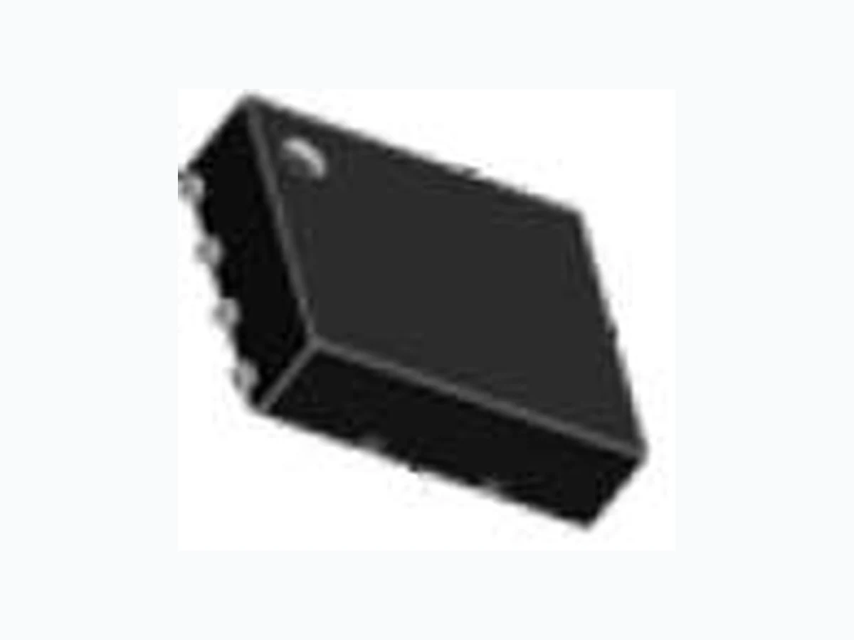
CSD95372BQ5MC Synchronous Buck NexFET™ Smart Power Stage datasheet (Rev. A)
Document overview
- Manufacturer or author: Texas Instruments, Incorporated [SLPS417,A]
- PDF pages: 12
Technical content
+Is1 -Is2 +Is2 -Is2 PWM2 VOUT SS RT VCC VOUT VOUT VIN Multiphase Controller CSD95372B CSD95372B PGND TSEN 0 10 20 30 40 50 60 100 Output Current (A) Efficiency (%) Power Loss (W) VDD = 5V VIN = 12V VOUT = 1.2V LOUT = .225µH fSW = 500kHz TA = 25ºC G001 Product Folder Sample & Buy T echnical Documents Tools & Software Support & Community CSD95372BQ5MC SLPS417A –APRIL 2014–REVISED JULY 2015 CSD95372BQ5MCSynchronousBuckNexFET™ SmartPowerStage
1 Features 2 Applications
1• 60-A Continuous Operating Current Capability • Multiphase Synchronous Buck Converters
- 93.4% System Efficiency at 30 A – High-Frequency Applications
- Low Power Loss of 2.8 W at 30 A – High-Current, Low Duty-Cycle Applications
- High-Frequency Operation (up to 1.25 MHz) • POL DC-DC Converters
- Diode Emulation Mode With FCCM • Memory and Graphic Cards
- Temperature-Compensated Bidirectional Current • Desktop and Server VR11.x / VR12.x V-Core and Sense Memory Synchronous Converters
- Analog Temperature Output (600 mV at 0°C)
3 Description• Fault Monitoring
The CSD95372BQ5MC NexFET™ smart power– High-Side Short, Overcurrent, and stage is a highly optimized design for use in a high-Overtemperature Protection power, high-density synchronous buck converter.
- 3.3-V and 5-V PWM Signal Compatible This product integrates the driver IC and Power MOSFETs to complete the power stage switching• Tri-State PWM Input function. This combination produces high-current,• Integrated Bootstrap Diode high-efficiency, and high-speed switching capability in
- Optimized Deadtime for Shoot-Through Protection a small 5 mm × 6 mm outline package. It also integrates the accurate current sensing and• High-Density SON 5 × 6 mm Footprint temperature sensing functionality to simplify system• Ultra-Low Inductance Package design and improve accuracy. In addition, the PCB• System-Optimized PCB Footprint footprint is optimized to help reduce design time and
- DualCool™ Packaging simplify the completion of the overall system design.
- RoHS Compliant – Lead-Free Terminal Plating Device Information(1)
- Halogen-Free DEVICE MEDIA QTY PACKAGE SHIP CSD95372BQ5MC 13-Inch Reel 2500 TapeSON 5 × 6 mm andDualCool PackageCSD95372BQ5MCT 7-Inch Reel 250 Reel (1) For all available packages, see the orderable addendum at the end of the data sheet. Application Diagram Typical Power Stage Efficiency and Power Loss An IMPORTANT NOTICE at the end of this data sheet addresses availability, warranty, changes, use in safety-critical applications, intellectual property matters and other important disclaimers. PRODUCTION DATA.
SLPS417A –APRIL 2014–REVISED JULY 2015 www.ti.com Table of Contents
4 Revision History
NOTE: Page numbers for previous revisions may differ from page numbers in the current version. Changes from Original (April 2014) to Revision A Page
2 Submit Documentation Feedback Copyright © 2014–2015, Texas Instruments Incorporated
Product Folder Links: CSD95372BQ5MC
BOOT_R VIN 6 7 PGND CSD95372BQ5MC www.ti.com SLPS417A –APRIL 2014–REVISED JULY 2015
5 Pin Configuration and Functions
DESCRIPTION
BOOT_R 8 Return path for HS gate driver, connected to VSW internally. Enables device operation. If ENABLE = logic HIGH, turns on device. If ENABLE = logic LOW, the device is turned ENABLE 3 off and both MOSFET gates are actively pulled low. An internal 100 kΩ pulldown resistor will pull the ENABLE pin LOW if left floating. This pin enables the Diode Emulation function. When this pin is held LOW, Diode Emulation Mode is enabled for FCCM 10 sync FET. When FCCM is HIGH, the device is operated in Forced Continuous Conduction Mode. An internal 5 µA current source will pull the FCCM pin to 3.3 V if left floating. IOUT 1 Output of current sensing amplifier. V(IOUT) – V(REFIN) is proportional to the phase current. PGND 4 Power ground, connected directly to pin 13. PGND 13 Power ground Pulse width modulated 3-state input from external controller. Logic LOW sets control FET gate low and sync FET PWM 12 gate high. Logic HIGH sets control FET gate high and sync FET gate low. Open or High Z sets both MOSFET gates low if greater than the tri-state shutdown hold-off time (t3HT). REFIN 2 External reference voltage input for current sensing amplifier Temperature Analog Output. Reports a voltage proportional to the die temperature. An ORing diode is integrated in bypassed to PGND with a 1 nF 16 V X7R ceramic capacitor. VDD 5 Supply voltage to gate driver and internal circuitry VIN 7 Input voltage pin. Connect input capacitors close to this pin. VSW 6 Phase node connecting the HS MOSFET source and LS MOSFET drain – pin connection to the output inductor. Copyright © 2014–2015, Texas Instruments Incorporated Submit Documentation Feedback 3 Product Folder Links: CSD95372BQ5MC
SLPS417A –APRIL 2014–REVISED JULY 2015 www.ti.com
6 Specifications
6.1 Absolute Maximum Ratings
TA = 25°C (unless otherwise noted)(1) MIN MAX UNIT VIN to PGND –0.3 25 V VIN to VSW –0.3 25 V VIN to VSW (10 ns) –7 27 V VSW to PGND –0.3 20 V VSW to PGND (10 ns) –7 23 V VDD to PGND –0.3 7 V ENABLE, PWM, FCCM. TAO, IOUT, REFIN to PGND –0.3 VDD + 0.3 V V BOOT to BOOT_R(2) –0.3 VDD + 0.3 V V PD Power dissipation 12 W TJ Operating junction –55 150 °C Tstg Storage temperature –55 150 °C (1) Stresses beyond those listed under Absolute Maximum Ratings may cause permanent damage to the device. These are stress ratings only, which do not imply functional operation of the device at these or any other conditions beyond those indicated under Recommended Operating Conditions. Exposure to absolute-maximum-rated conditions for extended periods may affect device reliability. (2) Should not exceed 7 V
6.2 ESD Ratings
Human body model (HBM) ±2000 V(ESD) Electrostatic discharge V Charged device model (CDM) ±500
6.3 Recommended Operating Conditions
TA = 25° (unless otherwise noted) MIN MAX UNIT VDD Gate drive voltage 4.5 5.5 V VIN Input supply voltage(1) 16 V VOUT Output voltage 5.5 V IOUT Continuous output current VIN = 12 V, VDD = 5V, VOUT = 3.3 V, 60 A ƒSW = 500 kHz, LOUT = 0.47 µH(2) IOUT-PK Peak output current(3) 90 A ƒSW Switching frequency CBST = 0.1 µF (min) 1250 kHz On time duty cycle ƒSW = 1 MHz 85% Minimum PWM on time 40 ns Operating temperature –40 125 °C (1) Operating at high VIN can create excessive AC voltage overshoots on the switch node (VSW) during MOSFET switching transients. For reliable operation, the switch node (VSW) to ground voltage must remain at or below the Absolute Maximum Ratings. (2) Measurement made with six 10-µF (TDK C3216X5R1C106KT or equivalent) ceramic capacitors placed across VIN to PGND pins. (3) System conditions as defined in Note 1. Peak Output Current is applied for tp = 50 µs
6.4 Thermal Information
TA = 25°C (unless otherwise noted) THERMAL METRIC MIN TYP MAX UNIT RθJC(top) Junction-to-case (top of package) thermal resistance (1) 5 °C/W RθJB Junction-to-board thermal resistance(2) 1.5 °C/W (1) RθJC(top) is determined with the device mounted on a 1 inch² (6.45 cm²), 2-oz (0.071 mm thick) Cu pad on a 1.5 inches x 1.5 inches, 0.06-inch (1.52 mm) thick FR4 board. (2) RθJB value based on hottest board temperature within 1 mm of the package.
4 Submit Documentation Feedback Copyright © 2014–2015, Texas Instruments Incorporated
Product Folder Links: CSD95372BQ5MC
VCORE_OUTPWM1 CSP1 VSP VSN PWM2 CSP2 PWM3 CSP3 PWM4 CSP4 TPS53661 SDIO SCLK ALERT#To/From CPU I2C or PMBus (Optional) SLEW-MODE ENABLE VR_RDY VR_HOT# VR_FAULT# ENABLE GND /c5e VR_FAULT# /c5e SKIP#-RAMP V3R3 V1212V 3.3V PMB_DIO PMB_CLK PMB_ALERT# COMP VREF B-TMAX O-USR ADDR TSEN IMONIMON F-IMAX ISUM OCP-I PWM5 CSP5 PWM6 CSP6 12V VIN BOOT BOOT_R VDD ENABLE PGND PGND VSW PWM FCCM IOUT REFIN TAO/FAULT 12V VIN BOOT BOOT_R VDD ENABLE PGND PGND VSW PWM FCCM IOUT REFIN TAO/FAULT 12V VIN BOOT BOOT_R VDD ENABLE PGND PGND VSW PWM FCCM IOUT REFIN TAO/FAULT 12V VIN BOOT BOOT_R VDD ENABLE PGND PGND VSW PWM FCCM IOUT REFIN TAO/FAULT 12V VIN BOOT BOOT_R VDD ENABLE PGND PGND VSW PWM FCCM IOUT REFIN TAO/FAULT 12V VIN BOOT BOOT_R VDD ENABLE PGND PGND VSW PWM FCCM IOUT REFIN TAO/FAULT CSD95372B CSD95372B CSD95372B CSD95372B CSD95372B CSD95372B CSD95372BQ5MC www.ti.com SLPS417A –APRIL 2014–REVISED JULY 2015
7 Application Schematic
Copyright © 2014–2015, Texas Instruments Incorporated Submit Documentation Feedback 5 Product Folder Links: CSD95372BQ5MC
SLPS417A –APRIL 2014–REVISED JULY 2015 www.ti.com
8 Device and Documentation Support
8.1 Community Resources
The following links connect to TI community resources. Linked contents are provided "AS IS" by the respective contributors. They do not constitute TI specifications and do not necessarily reflect TI's views; see TI's Terms of Use. TI E2E™ Online Community TI's Engineer-to-Engineer (E2E) Community. Created to foster collaboration among engineers. At e2e.ti.com, you can ask questions, share knowledge, explore ideas and help solve problems with fellow engineers. Design Support TI's Design Support Quickly find helpful E2E forums along with design support tools and contact information for technical support.
8.2 Trademarks
DualCool, NexFET, E2E are trademarks of Texas Instruments. All other trademarks are the property of their respective owners.
8.3 Electrostatic Discharge Caution
This integrated circuit can be damaged by ESD. Texas Instruments recommends that all integrated circuits be handled with appropriate precautions. Failure to observe proper handling and installation procedures can cause damage. ESD damage can range from subtle performance degradation to complete device failure. Precision integrated circuits may be more susceptible to damage because very small parametric changes could cause the device not to meet its published specifications.
8.4 Glossary
SLYZ022 — TI Glossary. This glossary lists and explains terms, acronyms, and definitions.
6 Submit Documentation Feedback Copyright © 2014–2015, Texas Instruments Incorporated
Product Folder Links: CSD95372BQ5MC
K e L b E d d1 d2 Exposed tie clip may vary A 0.300 x 45° Ɵ CSD95372BQ5MC www.ti.com SLPS417A –APRIL 2014–REVISED JULY 2015
9 Mechanical, Packaging, and Orderable Information
The following pages include mechanical, packaging, and orderable information. This information is the most current data available for the designated devices. This data is subject to change without notice and revision of this document. For browser-based versions of this data sheet, refer to the left-hand navigation.
9.1 Mechanical Drawing
b1 2.750 TYP 0.108 TYP b3 0.250 TYP 0.010 TYP e 0.500 TYP 0.020 TYP K 0.350 TYP 0.014 TYP Copyright © 2014–2015, Texas Instruments Incorporated Submit Documentation Feedback 7 Product Folder Links: CSD95372BQ5MC
0.350(0.014) 2.750 (0.108) 0.250 (0.010) 5.639 (0.222) 5.300 (0.209) 3.400 (0.134) 5.900 (0.232) 1.000 (0.039) 0.500 (0.020) 0.410 (0.016) 6.300 (0.248) 0.370 (0.015) 0.300 (0.012) 0.331(0.013) 0.550 (0.022) 2.800 (0.110) R0.127 (R0.005) 0.300 (0.012) CSD95372BQ5MC SLPS417A –APRIL 2014–REVISED JULY 2015 www.ti.com
9.2 Recommended PCB Land Pattern
- Dimensions are in mm (inches).
9.3 Recommended Stencil Opening
- Dimensions are in mm (inches). 2. Stencil thickness is 100 µm.
8 Submit Documentation Feedback Copyright © 2014–2015, Texas Instruments Incorporated
Product Folder Links: CSD95372BQ5MC
www.ti.com 6-Feb-2026 PACKAGING INFORMATION Orderable part number Status (1) Material type (2) Package | Pins Package qty | Carrier RoHS (3) Lead finish/ Ball material (4) MSL rating/ Peak reflow (5) Op temp (°C) Part marking (6) CSD95372BQ5MC Active Production VSON-CLIP (DMC) | 12 2500 | LARGE T&R ROHS Exempt SN Level-2-260C-1 YEAR -55 to 150 95372BMC CSD95372BQ5MC.A Active Production VSON-CLIP (DMC) | 12 2500 | LARGE T&R ROHS Exempt SN Level-2-260C-1 YEAR -55 to 150 95372BMC CSD95372BQ5MCT Active Production VSON-CLIP (DMC) | 12 250 | SMALL T&R ROHS Exempt SN Level-2-260C-1 YEAR -55 to 150 95372BMC CSD95372BQ5MCT.A Active Production VSON-CLIP (DMC) | 12 250 | SMALL T&R ROHS Exempt SN Level-2-260C-1 YEAR -55 to 150 95372BMC (1) Status: For more details on status, see our product life cycle. (2) Material type: When designated, preproduction parts are prototypes/experimental devices, and are not yet approved or released for full production. Testing and final process, including without limitation quality assurance, reliability performance testing, and/or process qualification, may not yet be complete, and this item is subject to further changes or possible discontinuation. If available for ordering, purchases will be subject to an additional waiver at checkout, and are intended for early internal evaluation purposes only. These items are sold without warranties of any kind. (3) RoHS values: Yes, No, RoHS Exempt. See the TI RoHS Statement for additional information and value definition. (4) Lead finish/Ball material: Parts may have multiple material finish options. Finish options are separated by a vertical ruled line. Lead finish/Ball material values may wrap to two lines if the finish value exceeds the maximum column width. (5) MSL rating/Peak reflow: The moisture sensitivity level ratings and peak solder (reflow) temperatures. In the event that a part has multiple moisture sensitivity ratings, only the lowest level per JEDEC standards is shown. Refer to the shipping label for the actual reflow temperature that will be used to mount the part to the printed circuit board. (6) Part marking: There may be an additional marking, which relates to the logo, the lot trace code information, or the environmental category of the part. Multiple part markings will be inside parentheses. Only one part marking contained in parentheses and separated by a "~" will appear on a part. If a line is indented then it is a continuation of the previous line and the two combined represent the entire part marking for that device. Important Information and Disclaimer:The information provided on this page represents TI's knowledge and belief as of the date that it is provided. TI bases its knowledge and belief on information provided by third parties, and makes no representation or warranty as to the accuracy of such information. Efforts are underway to better integrate information from third parties. TI has taken and continues to take reasonable steps to provide representative and accurate information but may not have conducted destructive testing or chemical analysis on incoming materials and chemicals. TI and TI suppliers consider certain information to be proprietary, and thus CAS numbers and other limited information may not be available for release. In no event shall TI's liability arising out of such information exceed the total purchase price of the TI part(s) at issue in this document sold by TI to Customer on an annual basis. Addendum-Page 1
PACKAGE MATERIALS INFORMATION www.ti.com 18-Apr-2024 TAPE AND REEL INFORMATION Reel Width (W1) REEL DIMENSIONS A0B0K0WDimension designed to accommodate the component lengthDimension designed to accommodate the component thicknessOverall width of the carrier tapePitch between successive cavity centersDimension designed to accommodate the component width TAPE DIMENSIONSK0 P1B0WA0Cavity QUADRANT ASSIGNMENTS FOR PIN 1 ORIENTATION IN TAPE Pocket QuadrantsSprocket HolesQ1Q1Q2Q2Q3Q3Q4Q4User Direction of Feed P1ReelDiameter *All dimensions are nominal Device Package Type Package Drawing Pins SPQ Reel Diameter (mm) Reel Width W1 (mm) (mm) (mm) (mm) (mm) W (mm) Pin1 Quadrant CSD95372BQ5MC VSON- CLIP CSD95372BQ5MCT VSON- CLIP Pack Materials-Page 1
PACKAGE MATERIALS INFORMATION www.ti.com 18-Apr-2024 TAPE AND REEL BOX DIMENSIONS Width (mm) W LH *All dimensions are nominal Device Package Type Package Drawing Pins SPQ Length (mm) Width (mm) Height (mm) CSD95372BQ5MC VSON-CLIP DMC 12 2500 367.0 367.0 38.0 CSD95372BQ5MCT VSON-CLIP DMC 12 250 213.0 191.0 35.0 Pack Materials-Page 2
IMPORTANT NOTICE AND DISCLAIMER TI PROVIDES TECHNICAL AND RELIABILITY DATA (INCLUDING DATASHEETS), DESIGN RESOURCES (INCLUDING REFERENCE DESIGNS), APPLICATION OR OTHER DESIGN ADVICE, WEB TOOLS, SAFETY INFORMATION, AND OTHER RESOURCES “AS IS” AND WITH ALL FAULTS, AND DISCLAIMS ALL WARRANTIES, EXPRESS AND IMPLIED, INCLUDING WITHOUT LIMITATION ANY IMPLIED WARRANTIES OF MERCHANTABILITY, FITNESS FOR A PARTICULAR PURPOSE OR NON-INFRINGEMENT OF THIRD PARTY INTELLECTUAL PROPERTY RIGHTS. These resources are intended for skilled developers designing with TI products. You are solely responsible for (1) selecting the appropriate TI products for your application, (2) designing, validating and testing your application, and (3) ensuring your application meets applicable standards, and any other safety, security, regulatory or other requirements. These resources are subject to change without notice. TI grants you permission to use these resources only for development of an application that uses the TI products described in the resource. Other reproduction and display of these resources is prohibited. No license is granted to any other TI intellectual property right or to any third party intellectual property right. TI disclaims responsibility for, and you fully indemnify TI and its representatives against any claims, damages, costs, losses, and liabilities arising out of your use of these resources. TI’s products are provided subject to TI’s Terms of Sale, TI’s General Quality Guidelines, or other applicable terms available either on ti.com or provided in conjunction with such TI products. TI’s provision of these resources does not expand or otherwise alter TI’s applicable warranties or warranty disclaimers for TI products. Unless TI explicitly designates a product as custom or customer-specified, TI products are standard, catalog, general purpose devices. TI objects to and rejects any additional or different terms you may propose. IMPORTANT NOTICE Copyright © 2026, Texas Instruments Incorporated Last updated 10/2025