
CS5208-1 CHERRY
Document overview
- Manufacturer or author: Provided By www.digicamel.com(FREE DATASHEET DOWNLOAD SITE)
- PDF pages: 7
Technical content
Features
3.3V @ 8A 300mF Load 200 124 0.1mF 100mF 5.0V Adj n 1.25V to 4.5V VOUT at 8A n Dropout Voltage < 1.0V @ 8A n 1.5% Trimmed Reference n Fast Transient Response n Thermal Shutdown n Current Limit n Short Circuit Protection Package Options CS5208-1 8A LDO 3-Pin Adjustable Linear Regulator CS5208-1
Description
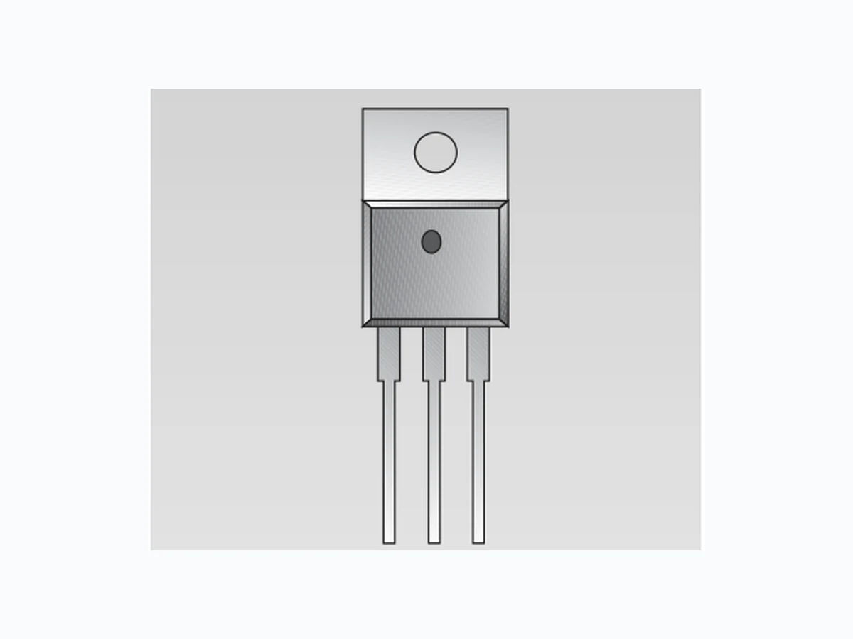
The CS5208-1 linear regulator pro- vides 8A at adjustable voltages from 1.25V to 4.5V. This adjustable device requires two external resis- tors to set the output voltage and provide the minimum load current for proper regulation. This regulator is intended for use as a post regulator and micropro- cessor supply. The fast loop response and low dropout voltage make this regulator ideal for appli- cations where low voltage opera- tion and good transient response are important. The circuit is designed to operate with dropout voltages as low as 1.0V at 8A. The regulator is protected against overload conditions with overcur- rent and thermal shutdown protection circuitry. The regulator is available in a TO-220 package. Applications Diagram
3 Lead TO-220
- Adjust 2. VOUT 3. VIN Tab = VOUT Cherry Semiconductor Corporation
2000 South County Trail, East Greenwich, RI 02818
Tel: (401)885-3600 Fax: (401)885-5786 Email: info@cherry-semi.com Web Site: www.cherry-semi.com A Company ¨ Rev. 6/11/97
PACKAGE PIN # PIN SYMBOL FUNCTION Electrical Characteristics: 0¡C²TA ² 70¡C, 0¡C²TJ ² 150¡C, VAdj = 0V unless otherwise specified. PARAMETER TEST CONDITIONS MIN TYP MAX UNIT CS5208-1 Absolute Maximum Ratings 3L TO-220 1 Adjust This pin is connected to the low side of the internally trimmed 1.5% bandgap reference voltage and carries a bias current of about 70µA. A resistor divider from Adj to V OUT and from Adj to ground sets the output voltage. Also, transient response can be improved by adding a small bypass capacitor from this pin to ground. OUT This pin is connected to the emitter of the power pass transistor and provides a regulated voltage capable of sourcing 8A of current. 3V IN This is the supply voltage for the regulator . For the device to regu- late, this voltage should be between 1.1V and 1.30V (depending on the output current) greater than the output voltage. Reference Voltage V (-1.5%) (+1.5%) Line Regulation V IN=2.75V to 5.5V, IOUT=10mA .02 .20 % Load Regulation V IN=2.75V,IOUT=10mA to 8A .04 .50 % Minimum Load Current V IN=5V, ÆVOUT= +1.5% 5 10 mA (Note 1) Adjust Pin Current V IN=2.75V,IOUT=10mA 70 120 µA Current Limit V IN=2.75V,ÆVOUT= -1.5% 8.1 9.0 A Short Circuit Current V IN=2.75V,VOUT=0V 6.0 8.5 A Ripple Rejection V IN=3.25V Avg, 60 80 dB (Note 2) V Ripple=1VP-P@120Hz, IOUT=4A,CAdj=0.1µF; COUT = 22µF Thermal Regulation (Note 2) 30ms Pulse, T A=25¡C 0.002 %/W Dropout Voltage I OUT=100mA 0.92 1.15 V (Minimum VIN -VOUT)I OUT=1A 0.93 1.15 V (Note 3) I OUT=2.75A 0.94 1.15 V IOUT=4A 0.95 1.15 V IOUT=8A 0.96 1.30 V RMS Output Noise Freq=10Hz to 10kHz, T A=25¡C 0.003 %V OUT Temperature Stability 0.5 % Thermal Shutdown (Note 4) 150 180 210 ¡C Thermal Shutdown Hysteresis 25 ¡C (Note 4) Note 1: The minimum load current is the minimum current required to maintain regulation. Normally the current in the resistor divider used to set the output voltage is selected to meet the minimum load current requirement. Note 2: This parameter is guaranteed by design and is not 100% production tested. Note 3: Dropout voltage is defined as the minimum input/output voltage differential required to maintain 1.5% regulation. Note 4: This parameter is guaranteed by design, but not parametrically tested in production. However, a 100% thermal shutdown functional test is performed on each part.
+ - +VREF CS5208-1 Typical Performance Characteristics 0 10 20 30 40 50 60 70 80 90 100 110 120 130 -0.150 -0.125 -0.100 -0.075 -0.050 -0.025 -0.000 0.025 0.050 0.075 0.100 TJ (°C) Output Voltage Deviation (%) IO=10mA VIN=2.75V Output Voltage Deviation (%) Output Current (A) TCase=0°C TCase =25°C TCase=125°C 0.00 8.00 0.000 0.200 0.225 0.250 0.175 0.150 0.125 0.100 0.075 0.050 0.025 0 10 20 30 40 50 60 70 80 90 100 110 120 130 60.00 65.00 70.00 75.00 80.00 85.00 90.00 TCase (°C) Adjust Pin Current (mA) IO=10mA Reference Voltage vs. Temperature Load Regulation vs. Output Current Adjust Pin Current vs Temperature 72.4 72.2 72.0 71.8 71.6 71.4 71.2 71.0 70.8 70.6 70.4 IOUT (A) Adjust Pin Current (mA) 70.2 70.0 72.6 2.4 4.8 8.0 Adjust Pin Current vs. IOUT
The CS5208-1 linear regulator has a composite PNP-NPN output stage that requires an output capacitor for stability. A detailed procedure for selecting this capacitor is includ- ed in the Stability Considerations section. Design Guidelines This LDO adjustable regulator has an output voltage range of 1.25V to 4.5V. An external resistor divider sets the out- put voltage as shown in Figure 1. The regulatorÕs voltage sensing error amplifier maintains a fixed 1.25V reference between the output pin and the adjust pin. A resistor divider network R 1 and R2 causes a fixed current to flow to ground. This current creates a voltage across R2 that adds to the 1.25V across R 1 and sets the overall output voltage. The adjust pin current (typically 50µA) also flows through R 2 and adds a small error that should be taken into account if precise adjustment of Vout is necessary. The output voltage is set according to the formula: VOUT = VREF ´ + R2 ´ IAdj The term IAdj ´ R2 represents the error added by the adjust pin current. R1 is chosen so that the minimum load current is a least 10mA. R1 and R2 should be of the same composition for best tracking over temperature. The divider resistors should be placed as close to the IC as possible and connect- ed to the output with a separate metal trace. R 1 + R2 Adjustable Operation Theory of Operation CS5208-1 20.0 18.0 16.0 14.0 12.0 10.0 8.0 6.0 4.0 2.0 0.0 Output Current (A) VIN-VOUT (V) 4.0 4.5 5.0 5.5 Dropout Voltage (V) Output Current (A) 0.00 0.25 0.50 0.75 1.00 1.25 Minimum Load Current (mA) VIN – VOUT (V) 0.80 0.82 0.88 0.90 0.98 1.00 TCASE = 23°C 0.84 0.86 0.92 0.94 0.96 TCASE = 125°C TCASE = 0°C Typical Performance Characteristics: continued Dropout Voltage vs. Output Current Short Circuit Current vs. VIN - VOUT Minimum Load Current vs. VIN - VOUT 101 102 103 104 105 20.0 30.0 50.0 70.0 90.0 Frequency (Hz) Ripple Rejection (dB) 80.0 60.0 40.0 10.0 VIN - VOUT = 2V VRipple = 1VPP IOUT = 4A CAdj = 0.1mF COUT = 22mF 106 Ripple Rejection vs. Frequency
ed to ground, damage can occur. In this case, a diode con- nected as shown in Figure 3 is recommended. A rule of thumb useful in determining if a protection diode is required is to solve for current I = , where I is the current flow out of the load capacitance when VIN is shorted, C is the value of the load capacitance, V is the output voltage, and T is the time duration required for V IN to transition from high to being shorted. If the calculated current is greater than or equal to the typi- cal short circuit current value provided in the specifica- tions, serious thought should be given to including a pro- tection diode. Figure 3. Current Limit The internal current limit circuit limits the output current under excessive load conditions and protects the regulator. Short Circuit Protection The device includes foldback short circuit current limit that clamps the output current at approximately two amperes less than its current limit value. Thermal Shutdown The thermal shutdown circuitry is guaranteed by design to become activated above a die junction temperature of 150¡C and to shut down the regulator output. This circuit- ry includes a thermal hysteresis circuit with 25¡C of typical hysteresis, thereby allowing the regulator to recover from a thermal fault automatically. Calculating Power Dissipation and Heat Sink Requirements High power regulators such as the CS5208-1 usually oper- ate at high junction temperatures. Therefore, it is important to calculate the power dissipation and junction tempera- tures accurately to ensure that an adequate heat sink is used. Since the package tab is connected to Vout on the CS5208-1, electrical isolation may be required for some applications. Also, as with all high power packages, ther- mal compound in necessary to ensure proper heat flow. For added safety, this high current LDO includes an inter- nal thermal shutdown circuit The thermal characteristics of an IC depend on the follow- ing four factors. Junction temperature, ambient tempera- ture, die power dissipation, and the thermal resistance from the die junction to ambient air. The maximum junc- tion temperature can be determined by: T J(max) = TA(max) + PD(max) ´ RQJA The maximum ambient temperature and the power dissi- pation are determined by the design while the maximum junction temperature and the thermal resistance depend on the manufacturer and the package type. The maximum power dissipation for a regulator is: PD (max) = (VIN(max) -VOUT(min))IOUT(max) + VIN(max) ´ IIN(max) A heat sink effectively increases the surface area of the package to improve the flow of heat away from the IC and into the surrounding air. Each material in the heat flow path between the IC and the outside environment has a thermal resistance which is measured in degrees per watt. Like series electrical resistances, these thermal resistances are summed to determine the total thermal resistance between the die junction and the surrounding air, R QJA. This total thermal resistance is comprised of three compo- nents. These resistive terms are measured from junction to case (R QJC), case to heat sink (RQCS), and heat sink to ambi- ent air (RQSA ). The equation is: RQJA = RQJC + RQCS + RQSA RQJC is rated @ 1.4¡C/W for the CS5208-1. For a high cur- rent regulator such as the CS5208-1 the majority of heat is generated in the power transistor section. The value for R QSA depends on the heat sink type, while the RQCS depends on factors such as package type, heat sink inter- face (is an insulator and thermal grease used?), and the contact area between the heat sink and the package. Once these calculations are complete, the maximum permissible value of R QJA can be calculated and the proper heat sink selected. For further discussion on heat sink selection, see our Cherry application note ÒThermal Management for Linear Regulators.Ó VOUTVIN CS5208-1 Adj C ´ V T Application Notes: continued
RQJC typ 1.4 ûC/W RQJA typ 50 ûC/W Rev. 6/11/97 © 1999 Cherry Semiconductor Corporation Package Specification PACKAGE DIMENSIONS IN mm (INCHES) Cherry Semiconductor Corporation reserves the right to make changes to the specifications without notice. Please contact Cherry Semiconductor Corporation for the latest available information. PACKAGE THERMAL DATA
Ordering Information
CS5208-1GT3 3L TO-220 Straight
3 Lead TO-220 (T) Straight
5.33 (.210) 4.83 (.190) 2.79 (.110) 2.29 (.090) 1.02 (.040) 0.63 (.025) 0.56 (.022) 0.38 (.014) 1.40 (.055) 1.14 (.045) 4.83 (.190) 4.06 (.160) 6.17 (.243) REF 1.14 (.045) 1.52 (.060) 1.14 (.045) 1.40 (.055) 2.87 (.113) 5.94 (.234) 14.22 (.560) 13.72 (.540) 2.92 (.115) 2.29 (.090) 9.78 (.385) 10.54 (.415) 3.71 (.146) 3.96 (.156) 14.99 (.590) 14.22 (.560)