

 Download PDF
CNA30E2200FB IXYS
Document overview
- PDF pages: 2
Technical content
Page 1
High Voltage Phase Control Thyristor
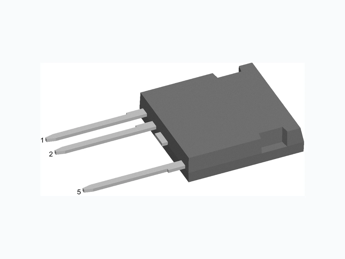
in High Voltage ISOPLUS i4-PAC™
5
Thyristor
Symbol Conditions
VDRM VDSM
VRRM / RSM
ITSM
sine 180°; t = 10 ms; VR = 0 V; TVJ = 25°C (di/dt)cr f = 50 Hz; tp = 200 µs; VD = 2000 V diG /dt = 0.45 A/µs; IG = 0.45 A non repetitive;
IT = 45 A
(dv/dt)cr VD = 2200 V RGK = ∞; method 1 (linear voltage rise)
CNA30E2200FB
VDRM = 2200 V ITSM = 200 A
2
1
Features
- high voltage thyristor
Maximum Ratings
- chip technology for long term stability
2200 V
- ISOPLUS i4-PAC™
2300 V high voltage package - isolated back surface
1650 V - enlarged creepage towards heatsink
200 A - enlarged creepage between high
150 A/µs
voltage pins - application friendly pinout - high reliability - industry standard outline
5000 V/µs
Characteristic Values
Symbol Conditions
| min. | max. |
|---|---|
| V I = 45 A T = 25°C T T VJ | 3.0 V |
| V GT V = 6 V T = 25°C I D VJ GT | 2.5 V 250 mA |
| V GD V = 2/ V T = 25°C I D 3 DRM VJ GD | 0.2 V 5 mA |
| I t = 10 µs; V = 6 V T = 0°C L p D VJ I = 0.45 A; di /dt = 0.45 A/µs G G | 700 mA |
| I V = 6 V; R = ∞ T = 0°C H D GK VJ T = 70°C 55 VJ | 300 mA mA |
| t I = 20 A; t = 300 µs; di/dt = -20 A/µs q T p V = 10 V; dv/dt = 20 V/µs R V = 800 V T = 70°C D VJ | 100 µs |
| I V = V ; V = V T = 25°C RRM / DRM R RRM D DRM VJ T = 70°C VJ | 50 µA 200 µA |
| I V = V ; V = V T = 70°C DSM / RSM R RSM D DSM VJ | 2 mA |
IXYS reserves the right to change limits, test conditions and dimensions.
20160523b
© 2016 IXYS All rights reserved
1 - 2
Page 2
CNA30E2200FB
Component
Maximum Ratings
Symbol Conditions
TVJ
-10 ... +70
°C
Tstg
-40 ... +70
°C
VISOL
IISOL < 1 mA; 50/60 Hz
2500 V~
FC Mounting force with clip
20...120
N
Characteristic Values
Symbol Conditions
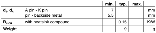
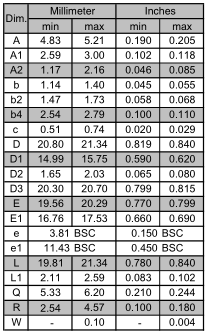
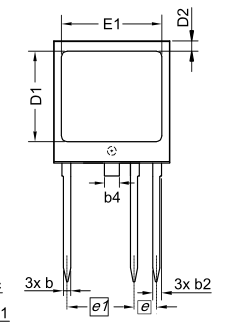
A
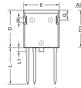
c
1 2
5
A1
W
IXYS reserves the right to change limits, test conditions and dimensions.
© 2016 IXYS All rights reserved
Die konvexe Form des Substrates ist typ. < 0.05 mmüber der Kunststoffoberflächeder Bauteilunterseite The convexbow of substrate is typ. < 0.05 mmover plastic surface level ofdevice bottom side
20160523b
2 - 2