
CEM3320 ETC
Document overview
- Manufacturer or author: Provided By www.digicamel.com(FREE DATASHEET DOWNLOAD SITE)
- PDF pages: 2
Technical content
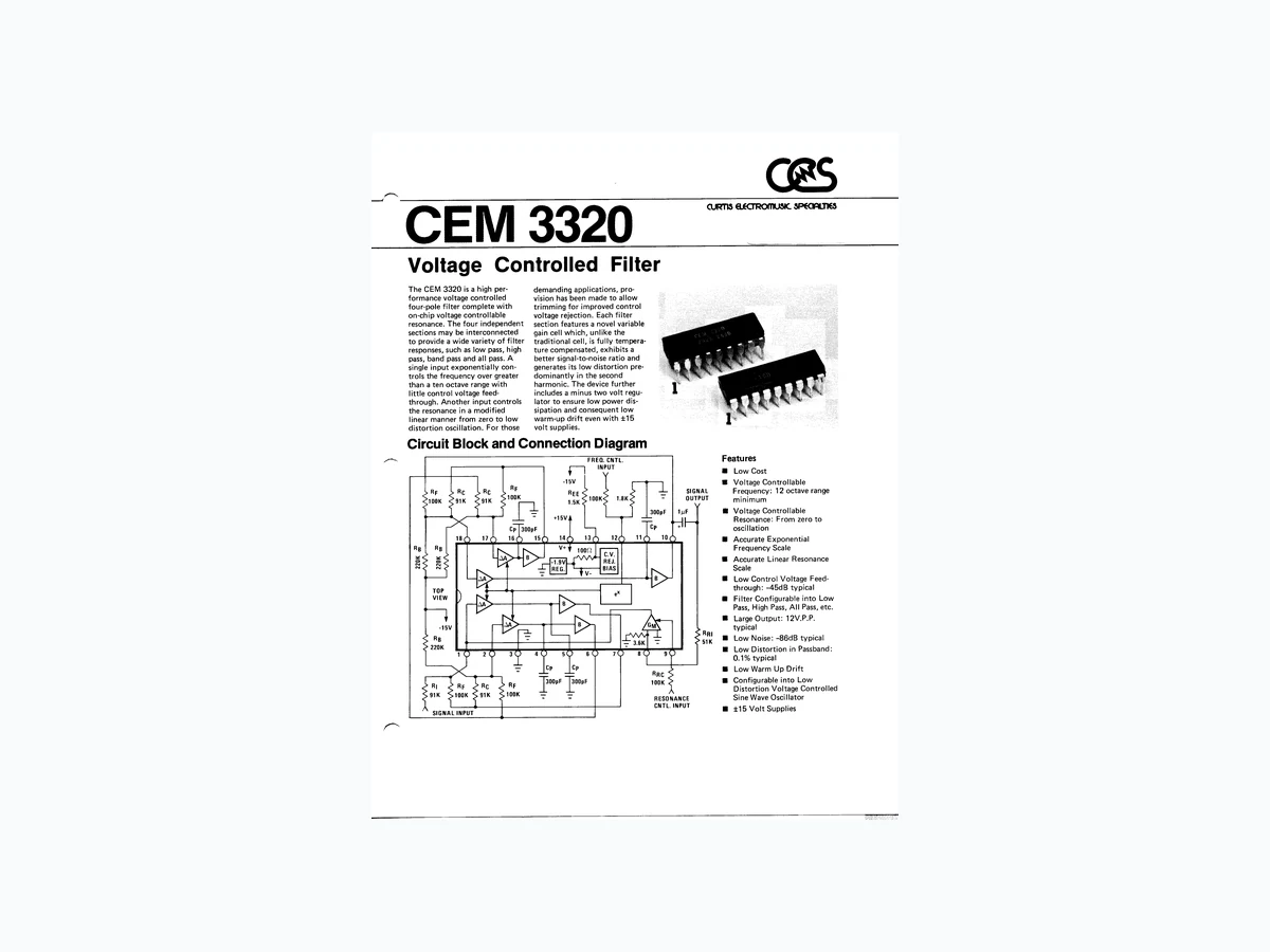
~ CRS fe Voltage Controlled Filter The CEM 3320 is a high per- demanding applications, pro- formance voltage controlled vision has been made to allow four-pole filter complete with trimming for improved control on-chip voltage controllable voltage rejection. Each filter resonance. The four independent section features a novel variable sections may be interconnected gain cell which, unlike the to provide a wide variety of filter traditional cell, is fully tempera- responses, such as low pass, high —_ ture compensated, exhibits a pass, band pass and all pass. A better signal-to-noise ratio and g oa single input exponentially con- generates its low distortion pre- 4 ‘ trols the frequency over greater dominantly in the second ib than a ten octave range with harmonic. The device further I z little control voltage feed- includes a minus two volt regu- i through. Another input controls —_ lator to ensure low power dis- ue: 2. the resonance in a modified sipation and consequent low linear manner from zero to low —_ warm-up drift even with £15, I distortion oscillation. For those —_ volt supplies. Circuit Block and Connection Diagram “~ FREQ. CNTL. Features ‘ mer ® Low Cost a “15 ® Voltage Controllable tk REE + SIGNAL Frequency: 12 octave range 100! 15K 5 100KS 1.8K = OUTPUT minimum [4 300pF | TUF ™@ Voltage Controllable +8V Resonance: From zero to Cp] 300pF oP * oscillation BO (oma Lo MaLL1@ 10 M10 ML 0 MLL © MLL) @ Accurate Exponential fe | RB Frequency Scale ws Ist oy, quency so py REJ. ™® Accurate Linear Resonance No 8 fal BIAS Scale > => ™@ Low Control Voltage Feed- Top through: ~45dB typical view |) Bo @ Filter Configurable into Low || Pass, High Pass, All Pass, etc. ™@ Large Output: 12V.P.P. OY PTIOP J lend || dee Me Re stk Low Noise: -86dB typical 220K SS fi a . TO eK 10 10 Nt 10 ar 10a or Te) © ™ Low Distortion in Passband: 0.1% typical = fp _|te Rac © Low Warm Up Drift R Re po pvr 100K ™@ Configurable into Low ork 100K Distortion Voltage Controlled > = RESONANCE Sine Wave Oscillator CNTL. INPUT i “* SIGNAL INPUT PO m 215 Volt Supplies
Electrical Characteristics
Voc = +15V Re = 100K Ta = 25°C Rea. yy inout le} Pole Frequency Control Range 3500:1 10,000:1 - {| Tax roan |ra + “UT nsv S| aK, Sensitivity of Pole Frequency OT] LL Control Scale, Midrange 57.5 60 625 | mV/decade potessteas Tempco of Pole Frequency . \\y Control Scale 3000 3300 3600 ppm aeer les stenay Exponential Error of-Pole BRAARAAA&E Frequency Control Scale? - 4 12 % " Sage oT ane Gain of Variable Gain Cell E Sum ta eon at Vo~0 0.7 09 13 [TT resonance Max Gain of Variable Gain Cell 24 3.0 3.6 Syonal nur caren Tempco of Variable Gain Cell2 - 500 1500 ppm FIGURE 2 MLPASS FILTER WITH VC RESONANCE Output Impedance of Gain Cell2 05 1.0 2.0 Mo. Pole Frequency Control F Feedthrough - 60 200 mv = nea Pole Frequency Warm-up Drift - 5 15 % | % Tey bisez ry wes S neo | SL | ee Gm of Resonance | w= [ramet] Contro! Element at IcR=100UA 8 1.0 1.2 mmhos || Gq mag ry si i” Amount of Resonance Obtainable ere. reerr en Before Oscillation 20 30 - ae A wt Resonance Control Feedthrough? ~ 0.2 1.5 Vv ‘ ae aa ‘Output Swing At Clipping 10 12 14 VPP. ™ ({™ Output Noise re Max Output4 -76 -86 - 4B we ae: ™ Rejection in Bandreject 73 83 - dB Pot aggonance Distortion in PassbandS.7 - O41 0.3 % somac erat Distortion in Bandreject®.7 - 0.3 1 % houme 3 nano ass eR won RouaNCE Distortion gf Sine Wave Oscillation’ - 0.5 15 % Internal Reference Current, IREF 45 63 85 uA — et Input Bias Current of Frequency ey Sux [P Control Input 0.2 05 15 uA cHE: eh Sa P| Input Impedance to Resonance ese | Signal Input 27 3.6 45 Ka 5! a= Buffer Slew Rate 15 3.0 ' Vius meiiesicn mals] 2 Buffer Input Bias Current [ ein (leE=8mA) #8 £30 £100 nA reer ee Buffer Sink Capability 4 5 63 mA J] Gis Buffer Output Impedance? 6 100 200 2 ny mee Positive Supply Range +9 = +18 v rt ‘anor Negative Supply Range? 4 = -18 Vv + ypu ou Positive Supply Current 3.8 5 6.5 mA URE ALLPASE FILTER WITH RESONANCE Note 1: -25mV < Vc < +155mV. Most of this error occurs in upper two octaves. Note 2: Vc = 0 Note 3: Untrimmed. 0 < IoR < 100A Note 4: Filter is connected as low pass and set for 20 KHz cut-off frequency. Note 5: Output signal is 348 below clipping point. Note 6: Output signal is 3dB below passband level, which is 3dB below clipping point. In general, this is worst case condition. Note 7: Distortion is predominantly second harmonic. Note 8: Sinewave is not clipped by first stage. Note 9: Current limiting resistor always required. CRS ~ CURTIS ELECTROMUSIC SPECIALTIES Covered by U.S. Patent #4,004,141. Curtis Electromusic Specialties (CES) assumes no responsibility for use of any circuitry described. No circuit licenses are implied. CES reserves the right, at any time without notice, to change said circuitry. Printed U.S.A. © 1980