
CDBFN120-HF_12 COMCHIP
Document overview
- Manufacturer or author: Provided By www.digicamel.com(FREE DATASHEET DOWNLOAD SITE)
- PDF pages: 4
Technical content
Features
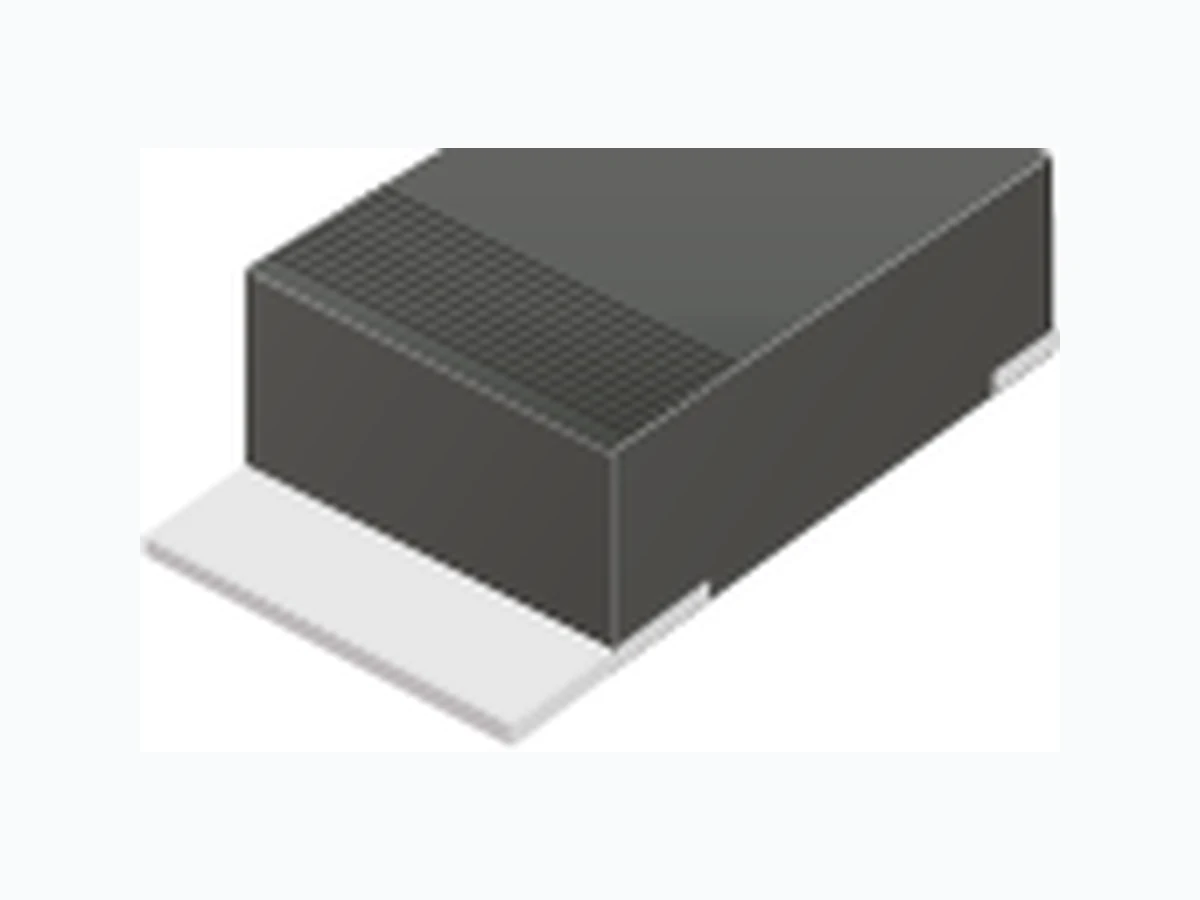
-Batch process design, excellent powe Mechanical data -Weight:0.008 gram(approx.). dissipation offers better reverse leakage current. -Low profile surface mounted application in order to optimize board space. -Low power loss, high efficiency. -High current capability, low forward voltage dorp. -High surge capability. -Guardring for overvoltage protection. -Very iny plastic SMD package. -Ultra high-speed switching. -Silicon epitaxial planarchip, metal silicon junction. -Lead-free parts meet environmental standards of MIL-STD-19500 /228 -Case: JEDEC SOD-323, Molded plastic -Terminals: Solde plated, solderable per MIL-STD-750, method 2026. -Polarity: Indicated by cathode band. -Mounting position: Any Reverse current on VR=VRRM @TA=25°C @TA=125°C CDBFN CDBFN CDBFN CDBFN 160-HF150-HF140-HF130-HF pF °C/W Maximum Ratings (at TA=25°C unless otherwise noted) 100 100 CDBFN CDBFN 1100-HF180-HF 0.85 0.012(0.3) Typ. 0.106 (2.70) 0.091 (2.30) 0.057 (1.45) 0.041 (1.05) 0.047 (1.2) 0.031 (0.8) Halogen free
Ratings and Characteristic Curves(CDBFN120-HF Thru CDBFN1100-HF) Page 2QW-JB001 Comchip Technology CO., LTD. Fig.2 Typical Forward Characteristics 0.01 IF, Instantaneous Forward Current (A) VF, Forward Voltage (V) 0.1 Fig.1 Typical Forward Current Derating Curve IO, Averaged Forward Current (A) TA, Ambient Temperature (O 0 100 Fig.3 Maximum Non-repetitive Peak Forward Surge Current Number of Cycles at 60Hz 1.0 1.5 1001.3 15050 200 0.5 IFSM, Peak Forward Surge Current (A) 1 100 0.1 O TJ=25 C Pulse width 300μs 1% duty cycle O TJ=25 C 8.3ms single half sine wave, JEDEC method Fig.4 Typical Junction Capacitance VR, Reverse Voltage (V) CJ, Junction Capacitance (pF) 350 0.01 100 200 150 300 0.1 10 100 250 Fig.5 Typical Reverse Characteristics Percent of Rated Peak Reverse Voltage (%) 0.01 IR, Reverse Current (mA) 100 0 14060 0.1 20 40 12080 100 O TJ=25 C O TJ=75 C SMD Schottky Barrier Rectifiers CDBFN150-HF~CDBFN160-HFCDBFN120-HF~CDBFN140-HF CDBFN120-HF~CDBFN140-HF CDBFN180-HF~CDBFN1100-HF CDBFN150-HF~CDBFN1100-HF REV:B
SMD Schottky Barrier Diode REV:B B C d D D2D1 SOD-323 SYMBOL A (mm) (inch) 2.44 MIN. 4.00 ± 0.10 1.50 ± 0.10 178 ± 1 SOD-323 SYMBOL (mm) E F P P0 P1 W W1 Reel Taping Specification o 120 Trailer Device Leader 10 pitches (min)10 pitches (min) T C Direction of Feed Index hole d E F B W P A D1 D2 D
REV:B Comchip Technology CO., LTD. SMD Schottky Barrier Diode Marking Code Park Number Marking Code X X QW-JB001 Suggested PAD Layout SIZE (inch) 1.500 (mm) 0.059 0.039 0.051 1.000 1.300 SOD-323 Standard Packaging Case Type Qty per Reel (Pcs) 3000SOD-323 Reel Size (inch) A B C A B C CDBFN120-HFCDBFN120-HF CDBFN130-HF CDBFN140-HF CDBFN150-HF CDBFN160-HF CDBFN180-HF CDBFN1100-HF