
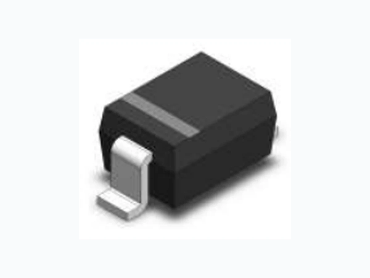
CD4148WSN LEIDITECH
Document overview
- Manufacturer or author: Provided By www.digicamel.com(FREE DATASHEET DOWNLOAD SITE)
- PDF pages: 2
Technical content
FEATURES
MARKING: T6, T4 Maximum Ratings and Electrical Characteristics, Single Diode @T A =25℃ Parameter Symbol Limits Unit Non-Repetitive Peak reverse voltage V RM 100 V Peak Repetitive Peak reverse voltage Working Peak Reverse Voltage DC Blocking Voltage V RRM V RWM V R 75 V RMS Reverse Voltage V R(RMS) 53 V Forward Continuous Current I FM 300 mA Average Rectified Output Current I O 150 mA Peak forward surge current @=1.0μs @ = 1 . 0 s I FSM 2.0 1.0 A Power Dissipation Pd 200 mW Thermal Resistance Junction to Ambient R θJA 625 ℃/W Junction temperature T j 125 ℃ Storage temperature T STG -65~+150 ℃ Electrical Ratings @T A =25℃ Parameter Symbol Min. Typ. Max. Unit Conditions V
0.715 V I
F =1mA V
0.855 V I
F =10mA V
1.0 V I
F =50mA Forward voltage V
1.25 V I
F =150mA I 1 μA V R =75V Reverse current I 25 nA V R =20V Capacitance between terminals C T 2 pF V R =0V,f=1MHz Reverse Recovery Time t rr 4 ns I F R =10mA Irr=0.1XI R L =100Ω CD4148WSN Dimensions SOD-323 Rev : 01.06.2014 1/2 www.leiditech.com
Shanghai Leiditech Electronic Co.,Ltd Email: sale1@leiditech.com Tel : +86- 021 50828806 Fax : +86- 021 50477059 Rev : 01.06.2014 2/2 www.leiditech.com Millimeters Inches Symbol Min. Nom. Max. Min. Nom. Max. 0.00 0.05 0.10 0.000 0.002 0.004 A3 0.15 REF 0.006 REF b 0.25 0.32 0.40 0.010 0.012 0.016 D 1.60 1.70 1.80 0.062 0.066 0.070 L 0.08 0.003 Symbol Millimeters Inches F 1.60 0.063 G 2.85 0.112 J 0.83 0.033 K 0.63 0.025 Soldering Footprint CD4148WSN