
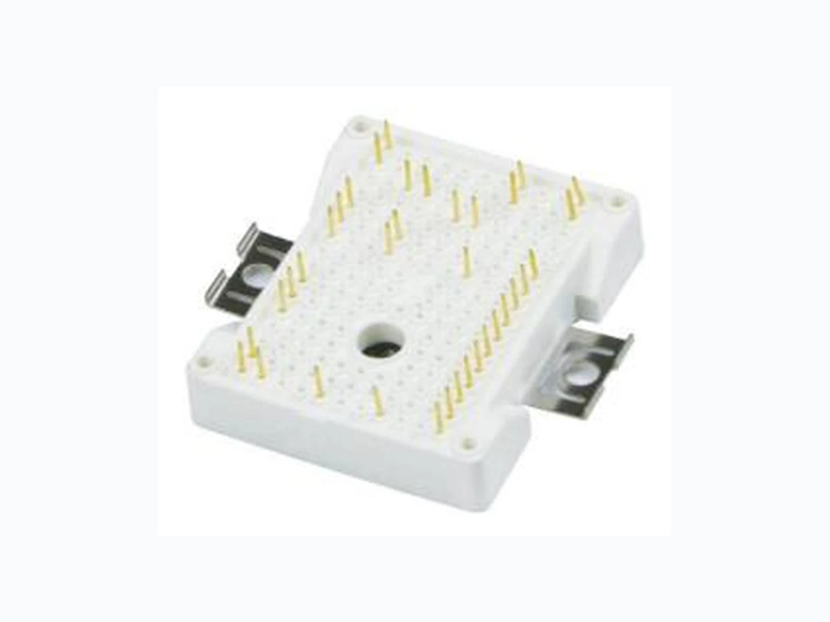
CCB016M12GM3 ISC
Document overview
- Manufacturer or author: Provided By www.digicamel.com(free datasheet download site)
- PDF pages: 7
Technical content
www.iscsemi.com 1
FEATURES
- VDS=1200V,RDS(on)=20.8mΩ(max)
- LowSwitchingLosses
- IntegratedNTCTemperatureSensor
- CompactDesign
APPLICATIONS
- HighFrequency SwitchingApplication
- UPS
- DC/ACConverters AbsoluteMaximumRatings(TC=25℃ unlessotherwisespecified) SYMBOL PARAMETER CONDITIONS VALUE UNIT VDS max Drain-SourceVoltage 1200 V VGS max Gate-SourceOpetationVoltage AbsoluteMaximumValues -8/+19 V VGS op Gate-SourceOpetationVoltage RecommendedOperationalValues -4/+15 V ID ContinuousDrainCurrent VGS=15V,THS=50℃,Tvj≤150℃ 50 A VGS=20V,THS=50℃,Tvj≤175℃ 50 A ID(pulsed) MaximumPulsedDrain-SourceCurrent VGS=15V,Tvj=25℃,tpmaxLimitedby Tvjmax 100 A Tvjop OperatingJunctionTemperature -40~150 ℃ Tvjmax MaximumJunctionTemperature 175 ℃ Ptot Totalpowerdissipation TH=80℃ 139 W
www.iscsemi.com 2 MOSFETChaRACTERISTICS(TC=25℃ unlessotherwisespecified) SYMBOL PARAMETER CONDITIONS MIN TYP. MAX UNIT V(BR)DSS Drain-SourceBreakdownVoltage VGS=0V; 1200 -- -- V VGS(th) GateThresholdVoltage VDS =VGS,ID =23mA 2.0 2.5 4.0 V VDS =VGS,ID =23mA,Tvj≤175℃ -- 2.0 -- RDS(on) Drain-SourceOn-stageResistance VGS=15V;ID=50A -- 16 20.8 mΩ VGS=15V;ID=50A;TJ=175°C -- 28.5 -- IGSS GateSourceLeakageCurrent VGS=15V;VDS=0V -- -- 0.5 uA IDSS ZeroGateVoltageDrainCurrent VDS =1200V,VGS =0V -- -- 38 uA Ciss InputCapacitance VGS =0V, VDS =1000V, f=1MHz, VAC=25mV -- 4210 -- pFCoss OutputCapacitance -- 260 -- Crss ReverseTransferCapacitance -- 18 -- Qg TotalGateCharge VDS =800V, ID=40A, VGS=-4V/+15V -- 274 -- nCQgs Gate-SourceCharge -- 75 -- Qgd Gate-DrainCharge -- 32 -- DiodeCharacteristics(TC=25℃ unlessotherwisespecified) SYMBOL PARAMETER CONDITIONS MIN TYP. MAX UNIT ISD DCBodyDiodeForwardCurrent VGS=-4V,TH=80℃ -- 43 -- A ISD pulse Pulsedbodydiodecurrent verifiedbydesign,tplimitedby Tvjmax -- -- 100 A VSD DiodeForwardVoltage ISD=50A -- 4.5 -- V ISD=50A;Tvj=150°C -- 4.1 --
www.iscsemi.com 3 MTCThermistor SYMBOL PARAMETER CONDITIONS MIN TYP. MAX UNIT R25 RatedResistance -- 5.0 -- KΩ ∆R/R DeviationofR100 TNTC=100,R100=493.3Ω -5 -- 5 % P25 Power Dissipation -- 20.0 -- mW B25/50 B-Value R2=R25exp[B25/50(1/T2-1/ ModuleCharacteristics(TC=25℃ unlessotherwisespecified) SYMBOL PARAMETER CONDITIONS MIN TYP. MAX UNIT Visol CaseIsolationVoltage t=1min,f=50Hz 3000 -- -- V Tjmax MaximumJunctionTemperature -- -- 175 ℃ Tvjop OperatingJunctionTemperature -40 -- 150 ℃ Tstg StorageTemperature -40 -- 125 ℃ LsCE StrayInductanceModule -- 8 -- nH RthJH ThermalResistance JunctiontoCase perMOSFET -- 0.62 0.68 K/W G WeightofModule -- 40 -- g
www.iscsemi.com 4 TypicalCharacteristics
www.iscsemi.com 5
www.iscsemi.com 6 CircuitDiagram
www.iscsemi.com 7 PackageDimensions(UNIT:MM): PRODUCTDISCLAIMER ISCreserves the rights tomakechangesof thecontent hereinthe datasheetatany timewithout notification.The informationcontained hereinis presentedonly as aguidefortheapplications ofour products. ISCproducts are intendedforusagein generalelectronic equipment.Theproducts are notdesigned for usein equipmentwhichrequire specialized qualityand/or reliability,orin equipment whichcould have applications inhazardous environments,aerospaceindustry,or medicalfield.Pleasecontactusif you intend ourproducts tobe used inthese specialapplications. ISCmakes nowarranty orguarantee regardingthe suitabilityof its products foranyparticularpurpose, nordoes ISCassumeanyliability arisingfrom theapplication oruse ofanyproducts, and specifically disclaimsany and allliability,includingwithout limitation special,consequential orincidental damages.