

 Download PDF
C7500-50 HAMAMATSU
Document overview
- PDF pages: 2
Technical content
Page 1
Near Infrared 1/2-inch
CCD Video Camera
DATA SHEET
C7500-50, -51
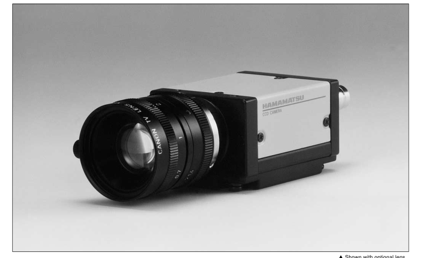
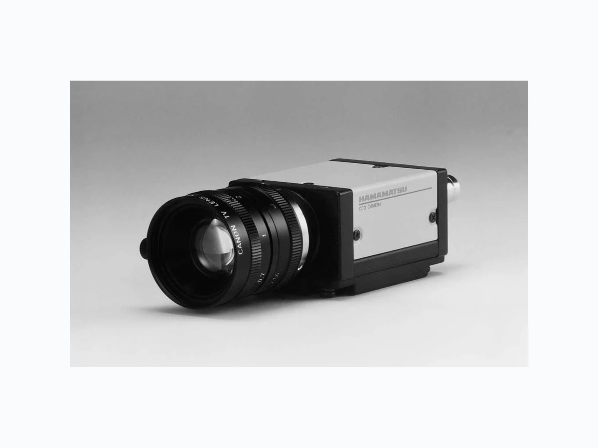
The C7500 incorporates a new 1/2-inch interline CCD with high sensitivity in the near-infrared region, 770 nm to 1100 nm, which surpasses that of conventional CCD cameras.
[Spectral Response Characteristic]
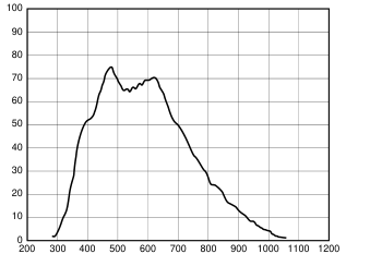
Wavelength (nm) \*This is typical, not guaranteed
L Shown with optional lens.
FEATURES
High Sensitivity in the Near-
G
Infrared Region
G High S/N Ratio
C7500-50 : 56 dB(EIA) C7500-51 : 54 dB(CCIR)
Small Readout Noise
G
High Resolution
G C7500-50 : 570(H) × 485(V) TV Line(EIA) C7500-51 : 560(H) × 575(V) TV Line(CCIR)
On-chip Integration
G A dedicated camera control unit enables images to be accumulated on the CCD chip with improved sensitivity.
Page 2
SPECIFICATIONS
| Type no. | C7500-50 | C7500-51 | |
|---|---|---|---|
| Pickup device | 1/2" Interline transfer CCD | ||
| Scan type | Interrace scan | ||
| Number of pixels (H) × (V) | 768 × 494 | 752 × 582 | |
| Cell size (H × V) µm | 8.4 × 9.8 | 8.6 × 8.3 | |
| Effective number of pixels | 756 × 485 | 739 × 575 | |
| Resolution (H) × (V)TV lines | 570 × 485 | 560 × 575 | |
| Lens mount (F,B) | C-mount (17.526 mm) | ||
| Sync system | EIA | CCIR | |
| Internal sync | Yes | ||
| External sync | HD/VD | Yes | |
| SYNC | Yes | ||
| R.R. | Yes | ||
| Impedance | 75 Ω (High) | ||
| AGC | ON / OFF / Fixed | ||
| Gamma | 1 / 0.45 | ||
| Camera output | Video (HD / VD) | ||
| Minimum sensitivity | 1 lux, F1.4, (AGC = ON, γ = OFF) | ||
| Power requirements | DC 12 V (12P) | ||
| Power consumption | 2.0 W | ||
| Typical sensitivity | 400 lux, F16 (2856 K) | ||
| S/N ratio | 56 dB | 54 dB | |
| Electronic shutter | Flickerless, 1/125 to 1/10,000 sec. | ||
| On-chip Integration | Yes | ||
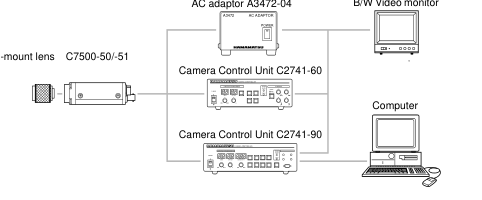
SYSTEM CONFIGURATION EXAMPLES
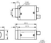
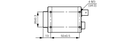
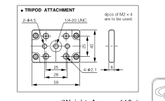
DIMENSIONAL OUTLINES
(UNIT: mm)
G The system can be configured to accommodate various applications,
including image acquisition, image enhancement, image improve-
ment, image measurement, and image filing.
44
B/W Video monitor
AC adaptor A3472-04
(Weight: Approx. 110g)
ISO 9001 Certificate: 09 105 79045
# Product and software package names noted in this documentation are trademarks or registered trademarks of their respective manufacturers. G Subject to local technical requirements and regulations, availability of products included in this promotional material may vary. Please consult with our sales office. G Information furnished by HAMAMATSU is believed to be reliable. However, no responsibility is assumed for possible inaccuracies or omissions. Specifications and external appearance are subject to change without notice.. © 2000 Hamamatsu Photonics K.K.
Homepage Address http://www.hamamatsu.com
HAMAMATSU PHOTONICS K.K., Systems Division 812 Joko-cho, Hamamatsu City, 431-3196, Japan, Telephone: (81)53-431-0124, Fax: (81)53-435-1574, E-mail:export@sys.hpk.co.jp U.S.A. and Canada: Hamamatsu Photonic Systems: 360 Foothill Road, Bridgewater, N.J. 08807-0910, U.S.A., Telephone: (1)908-231-1116, Fax: (1)908-231-0852, E-mail: usa@hamamatsu.com Germany: Hamamatsu Photonics Deutschland GmbH: Arzbergerstr. 10, D-82211 Herrsching am Ammersee, Germany, Telephone: (49)8152-375-0, Fax: (49)8152-2658, E-mail: info@hamamatsu.de
,
France: Hamamatsu Photonics France S.A.R.L.: 8, Rue du Saule Trapu, Parc du Moulin de Massy, 91882 Massy Cedex, France, Telephone: (33)1 69 53 71 00, Fax: (33)1 69 53 71 10, E-mail: infos@hamamatsu.fr United Kingdom: Hamamatsu Photonics UK Limited: 2 Howard Court, 10 Tewin Road, Welwyn Garden City, Hertfordshire, AL7 1BW, U.K., Telephone: (44) 1707-294888, Fax: (44) 1707-325777, E-mail: info@hamamatsu.co.uk North Europe: Hamamatsu Photonics Norden AB: Smidesvägen 12, SE-171-41 Solna, Sweden, Telephone: (46)8-509-031-00, Fax: (46)8-509-031-01, E-mail: info@hamamatsu.se
-
Italy: Hamamatsu Photonics Italia S.R.L.: Strada della Mois, 1/E 20020 Arese (Milano), Italy, Telephone: (39)02-935 81 733, Fax: (39)02-935 81 741, E-mail: info@hamamatsu.it
Cat. No. SICS1086E01 AUG/2001 HPK Created in Japan (PDF)