
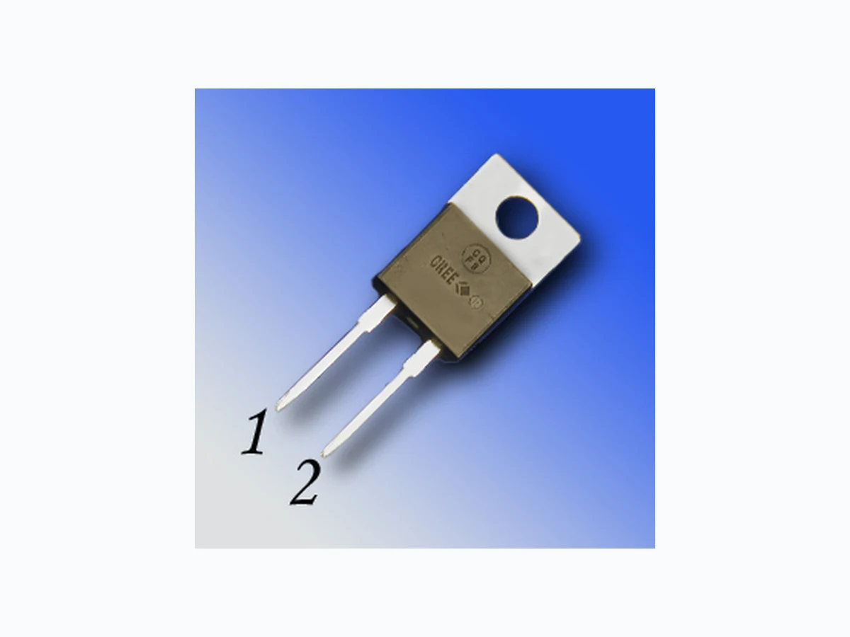
C2D10120 ETC1
Document overview
- Manufacturer or author: Provided By www.digicamel.com(FREE DATASHEET DOWNLOAD SITE)
- PDF pages: 5
Technical content
Features
1200-Volt Schottky Rectifier Zero Reverse Recovery Zero Forward Recovery High-Frequency Operation Temperature-Independent Switching Behavior Extremely Fast Swtitching Positive Temperature Coefficient on VF Benefits Replace Bipolar with Unipolar Rectifiers Essentially No Switching Losses Higher Efficiency Reduction of Heat Sink Requirements Parallel Devices Without Thermal Runaway
Applications
Switch Mode Power Supplies Power Factor Correction Motor Drives Package TO-220-2 Maximum Ratings Symbol Parameter Value Unit Test Conditions Note VRRM Repetitive Peak Reverse Voltage 1200 V VRSM Surge Peak Reverse Voltage 1200 V VDC DC Blocking Voltage 1200 V IF(AVG) Average Forward Current 10
22 A TC=160˚C
TC=125˚C IF(Peak) Peak Forward Current 25 A TC=125˚C, TREP<1 mS, Duty=0.5 IFRM Repetitive Peak Forward Surge Current 50 A TC=25˚C, tP=8.3 ms, Half Sine Wave IFSM Non-Repetitive Peak Forward Surge Current 250 A TC=25˚C, tP=10 µs, Pulse Ptot Power Dissipation 312
104 W TC=25˚C
TC=125˚C TJ , Tstg Operating Junction and Storage Temperature -55 to +175 ˚C PIN 1 PIN 2 CASE Part Number Package Marking C2D10120A TO-220-2 C2D10120
2 C2D10120 Rev. -
Electrical Characteristics
Symbol Parameter Typ. Max. Unit Test Conditions Note VF Forward Voltage 1.6 2.5 1.8
3.0 V IF = 10 A TJ=25°C
IF = 10 A TJ=175°C IR Reverse Current 10 200 1000 μA VR = 1200 V TJ=25°C VR = 1200 V TJ=150°C QC Total Capacitive Charge 61 nC VR = 1200 V, IF = 10 A di/dt = 500 A/μs TJ = 25°C C Total Capacitance 1000 pF VR = 0 V, TJ = 25°C, f = 1 MHz VR = 200 V, TJ = 25˚C, f = 1 MHz VR = 400 V, TJ = 25˚C, f = 1 MHz Note: This is a majority carrier diode, so there is no reverse recovery charge. Thermal Characteristics Symbol Parameter Typ. Max. Unit Test Conditions Note RθJC Thermal Resistance from Junction to Case 0.48 °C/W Typical Performance Figure 1. Forward Characteristics Figure 2. Reverse Characteristics
C2D10120 Rev. - Package Dimensions Package TO-220-2 A C E D G H B J L M N F P Q S T U V W X Y M in M ax M in M ax A .395 .410 10.033 10.414 B .235 .255 5.969 6.477 C .102 .112 2.591 2.845 D .337 .337 8.560 8.560 E .590 .610 14.986 15.494 F .149 .153 3.785 3.886 G 1.127 1.147 28.626 29.134 H .530 .550 13.462 13.970 J L .028 .036 .711 .914 M .045 .055 1.143 1.397 N .195 .205 4.953 5.207 P .170 .180 4.318 4.572 Q .048 .054 1.219 1.371 S 3° 5° 3° 5° T 3° 5° 3° 5° U 3° 5° 3° 5° V .100 .110 2.54 2.794 W .014 .021 .356 .533 X 3° 5° 3° 5° Y .395 .410 10.033 10.414 Z .130 .150 3.302 3.810 Inches M illim etersP OS R0.010 R 0.254 1 2 Z POS Inches Millimeters Min Max Min Max A .381 .410 9.677 10.414 B .235 .255 5.969 6.477 C .100 .120 2.540 3.048 D .223 .337 5.664 8.560 E .590 .615 14.986 15.621 F .143 .153 3.632 3.886 G 1.105 1.147 28.067 29.134 H .500 .550 12.700 13.970 J R 0.197 R 0.197 L .025 .036 .635 .914 M .045 .055 1.143 1.397 N .195 .205 4.953 5.207 P .165 .185 4.191 4.699 Q .048 .054 1.219 1.372 S 3° 6° 3° 6° T 3° 6° 3° 6° U 3° 6° 3° 6° V .094 .110 2.388 2.794 W .014 .025 .356 .635 X 3° 5.5° 3° 5.5° Y .385 .410 9.779 10.414 z .130 .150 3.302 3.810 NOTE: Dimension L, M, W apply for Solder Dip Finish
C2D10120 Rev. - This product has not been designed or tested for use in, and is not intended for use in, applications implanted into the human body nor in applications in which failure of the product could lead to death, personal injury or property damage, including but not limited to equipment used in the operation of nuclear facilities, life-support machines, cardiac defibrillators or similar emergency medical equipment, aircraft navigation or communication or control systems, air traffic control systems, or weapons systems. Copyright © 2006 Cree, Inc. All rights reserved. The information in this document is subject to change without notice. Cree, the Cree logo, and Zero Recovery are registered trademarks of Cree, Inc. Cree, Inc.
4600 Silicon Drive
Durham, NC 27703 USA Tel: +1.919.313.5300 Fax: +1.919.313.5451 www.cree.com/power Recommended Solder Pad Layout TO-220-2 Part Number Package Marking C2D10120A TO-220-2 C2D10120