


 Download PDF
LM25007 TI
Document overview
- PDF pages: 23
Technical content
Page 1
LM25007 42V, 0.5A Step-Down Switching Regulator
FEATURES
- Integrated 0.74Ω N-Channel MOSFET Switch
- Guaranteed 0.5A Output Current
- Ultra-Fast Transient Response
- Up to 800kHz Operation
- No Control Loop Compensation Required
- Vin Feed Forward Provides Constant Operating Frequency
- 2% Accurate 2.5V Feedback from -40°C to 125°C
- Highly Efficient Operation
- Intelligent Current Limit Protection
- External Shutdown Control
- Thermal Shutdown
- VSSOP and Thermally Enhanced WSON Packages
TYPICAL APPLICATIONS
- 12VDC and 24VDC Distributed Rail Systems
- 24VAC Systems
- Automotive Body Electronics and Telematics
- Industrial Systems
- HB-LED Constant Current Source
- Package:
– VSSOP-8
– WSON-8 (4mm x 4mm)
DESCRIPTION
The LM25007 is a monolithic step-down switching regulator featuring all of the functions needed to implement a low cost, efficient, power supply. Capable of driving a 0.5A load over a 9V-42V input voltage range, this device is easy to apply and is provided in the small VSSOP-8 and the thermally enhanced WSON-8 packages. Ultra-fast transient response is achieved through the use of a constant on-time architecture with Vin feed forward. This feature provides an almost constant operating frequency over load and input voltage variations. The operating frequency can be adjusted with a single resistor. This architecture is easy to use and tolerant of component selection. An intelligent current limit is
implemented in the LM25007 with forced off time that is inversely proportional to Vout thus ensuring recovery from fault conditions. The output voltage may be set from 2.5V to >30V. To improve efficiency in light load applications, the Vcc pin can be connected to an external voltage source to eliminate the drop through the internal regulator. Additional features include: thermal shutdown, Vcc undervoltage lockout, gate drive under-voltage lockout, and max duty cycle limiter.
Please be aware that an important notice concerning availability, standard warranty, and use in critical applications of Texas Instruments semiconductor products and disclaimers thereto appears at the end of this data sheet. All trademarks are the property of their respective owners. PRODUCTION DATA information is current as of publication date. Products conform to specifications per the terms of the Texas Instruments standard warranty. Production processing does not necessarily include testing of all parameters.
Page 2
Basic Step-Down Regulator
| Column 1 | Column 2 |
|---|---|
| ± 42V nput VIN | LM25007 |
| C1 |
VCC 7 C3
BST 2
GND
C4 L1
SW
VOUT
1 D1
R5 R3
FB
C2
R4
5
GND
Connection Diagram
| Column 1 | Column 2 | Column 3 |
|---|---|---|
| 1 | SW VIN BST VCC RCL RON RTN FB | 8 |
| 2 | 7 | |
| 3 | 6 | |
| 4 | 5 | |
8-Lead VSSOP, WSON
Page 3
Pin Descriptions
| Pin | Name | Description | Application Information |
|---|---|---|---|
| 1 | SW | Switching Node | Power switching node. Connect to the inductor, bootstrap capacitor, and free-wheeling diode. |
| 2 | BST | Boost Boot–strap capacitor input | An external capacitor is required between the BST and the SW pins. A 0.01µF ceramic capacitor is recommended. |
| 3 | RCL | Current Limit OFF time programming pin | A resistor between this pin and RTN sets the off-time when current limit is detected. The off-time is preset to 17 µs if FB = 0V . |
| 4 | RTN | Circuit Ground | |
| 5 | FB | Feedback Signal from Regulated Output | This pin is connected to the inverting input of the internal regulation comparator. The regulation threshold is 2.5V. |
| 6 | RON/SD | On-time set pin | A resistor between this pin and VIN sets the switch on-time as a function of Vin. The minimum recommended on-time is 300ns at the maximum input voltage. |
| 7 | VCC | Output from the internal high voltage bias regulator. | If an auxiliary voltage is available to raise the voltage on this pin above the regulation setpoint (7V), the internal series pass regulator will shutdown, reducing the IC power dissipation. Do not exceed 14V. This output provides gate drive power for the internal Buck switch. An internal diode is provided between this pin and the BST pin. A local 0.1uF decoupling capacitor is recommended. |
| 8 | VIN | Input supply voltage | Recommended operating range: 9V to 42V. |
| - | EP | Exposed pad, underside of the WSON package option | Exposed metal pad on the WSON package underside. It is recommended to connect this pad to the PC board ground plane to aid in heat dissipation. |
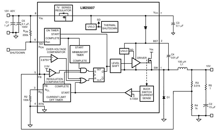
Typical Application Circuit and Block Diagram
Page 4
These devices have limited built-in ESD protection. The leads should be shorted together or the device placed in conductive foam during storage or handling to prevent electrostatic damage to the MOS gates.
Absolute Maximum Ratings(1)
| Column 1 | Column 2 |
|---|---|
| VIN to RTN | 45V |
| BST to RTN | 59V |
| SW to RTN (Steady State) | -1V |
| ESD Rating, Human Body Model(2) | 2kV |
| BST to V CC | 45V |
| BST to SW | 14V |
| VCC to RTN | 14V |
| All Other Inputs to RTN | -0.3 to 7V |
| Storage Temperature Range | -65°C to +150°C |
(1) Absolute Maximum Ratings are limits beyond which damage to the device may occur. Operating Ratings are conditions under which operation of the device is intended to be functional. For guaranteed specifications and test conditions, see the Electrical Characteristics. (2) The human body model is a 100pF capacitor discharge through a 1.5kΩ resistor into each pin. The human body ESD compliance level for Pin 7 and 8 is 1000V.
Operating Ratings(1)
| Column 1 | Column 2 |
|---|---|
| V IN | 9V to 42V |
| Junction Temperature | −40°C to + 125°C |
(1) Absolute Maximum Ratings are limits beyond which damage to the device may occur. Operating Ratings are conditions under which operation of the device is intended to be functional. For guaranteed specifications and test conditions, see the Electrical Characteristics.
Page 5
Electrical Characteristics(1)
Specifications with standard type are for TJ = 25°C only; limits in boldface type apply over the full Operating Junction Temperature (TJ) range. Minimum and Maximum limits are guaranteed through test, design, or statistical correlation. Typical values represent the most likely parametric norm at TJ = 25°C, and are provided for reference purposes only. Unless otherwise stated the following conditions apply: VIN = 24V, RON = 200kΩ. .
| Symbol | Parameter | Conditions | Min | Typ | Max | Unit |
|---|---|---|---|---|---|---|
| Startup Regulator | ||||||
| V Reg CC | V Regulator Output CC | 6.6 | 7 | 7.4 | V | |
| V Current Limit CC | (2) | 11 | mA | |||
| V Supply CC | ||||||
| V undervoltage Lockout Voltage CC (V increasing) CC | 6.3 | V | ||||
| V Undervoltage Hysteresis CC | 206 | mV | ||||
| V UVLO Delay (filter) CC | 3 | µs | ||||
| Operating Current (I ) CC | Non-Switching, FB = 3V | 500 | 675 | µA | ||
| Shutdown/Standby Current | RON/SD = 0V | 70 | 150 | µA | ||
| Switch Characteristics | ||||||
| Buck Switch Rds(on) | I = 200mA, TEST VBST −VSW = 6.3V(3) | 0.74 | 1.34 | Ω | ||
| Gate Drive UVLO (VBST – VSW) | Rising | 3.4 | 4.5 | 5.5 | V | |
| Gate Drive UVLO Hysteresis | 400 | mV | ||||
| Current Limit | ||||||
| Current Limit Threshold | 535 | 725 | 900 | mA | ||
| Current Limit Response Time | I Overdrive = 0.1A Time to switch Switch Off | 225 | ns | |||
| OFF time generator (test 1) | FB=0V, RCL = 100K | 17 | µs | |||
| OFF time generator (test 2) | FB=2.3V, RCL = 100K | 2.65 | µs | |||
| On Time Generator | ||||||
| TON -1 | Vin = 10V Ron = 200K | 2.15 | 2.77 | 3.5 | µs | |
| TON -2 | Vin = 40V Ron = 200K | 450 | 615 | 810 | ns | |
| Remote Shutdown Threshold | Rising | 0.45 | 0.7 | 1.1 | V | |
| Remote Shutdown Hysteresis | 40 | mV | ||||
| Minimum Off Time | ||||||
| Minimum Off Timer | FB = 0V | 300 | ns | |||
| Regulation and OV Comparators | ||||||
| FB Reference Threshold | Internal reference Trip point for switch ON | 2.445 | 2.5 | 2.550 | V | |
| FB Over-Voltage Threshold | Trip point for switch OFF | 2.875 | V | |||
| FB Bias Current | 100 | nA | ||||
| Thermal Shutdown | ||||||
| Tsd | Thermal Shutdown Temp. | 165 | °C | |||
| Thermal Shutdown Hysteresis | 25 | °C | ||||
| Thermal Resistance | ||||||
| θ JA | Junction to Ambient | DGK Package | 200 | °C/W | ||
| NGT Package | 40 | °C/W |
(1) All limits are guaranteed. All electrical characteristics having room temperature limits are tested during production with TA = TJ = 25°C. All hot and cold limits are guaranteed by correlating the electrical characteristics to process and temperature variations and applying statistical process control. (2) The VCC output is intended as a self bias for the internal gate drive power and control circuits. Device thermal limitations limit external loading. (3) For devices procured in the WSON-8 package the Rds(on) limits are guaranteed by design characterization data only.
Page 6
Typical Performance Characteristics
Operational Waveforms
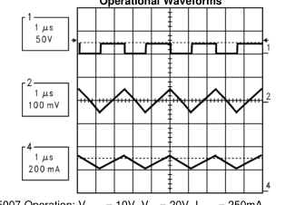
LM25007 Operation: VOUT = 10V, VIN = 20V, IOUT = 250mA CH1: Switch Node, CH2: VOUT (AC), CH4: Inductor Current
Figure 1.
LM25007 10V Output Efficiency
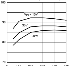
0 100 200 300 400 500
LOAD CURRENT (mA)
Figure 3.
Operational Waveforms
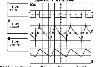
LM25007 Operation: VOUT = 10V, VIN = 42V, IOUT = 250mA CH1: Switch Node, CH2: VOUT (AC), CH4: Inductor Current
Figure 2.
Current Limit Off-Time vs VFB
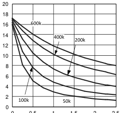
0 0.5 1 1.5 2 2.5
VFB (V) Figure 4.
VIN vs TON RON = 100k, 200k, 300k
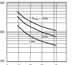
10000
1000
30 42
0
20 10 INPUT VOLTAGE VIN (V) Figure 5.
Page 7
DETAILED OPERATING DESCRIPTION
The LM25007 is a monolithic step-down switching regulator featuring all of the functions needed to implement low cost, efficient, power supply. Capable of driving a 0.5Amp load over a 9-42V input voltage range, this device is easy to apply and is provided in the small VSSOP-8 and the thermally enhanced WSON-8 packages. Ultra-fast transient response is achieved through the use of a constant on-time architecture with Vin feed forward. This feature provides and almost constant operating frequency over load and input voltage variations. The operating frequency may be adjusted up to 800kHz depending on input and output voltages. This architecture is easy to
use and tolerant of component selection. An intelligent current limit is implemented in the LM25007 with forced off time that is inversely proportional to Vout to ensure recovery from fault conditions. The output voltage may be set from 2.5V to >30V. To improve efficiency in light load applications, the Vcc pin can be tied to an external voltage source thus eliminating the drop through the integrated internal regulator. Additional protection features include: thermal shutdown, Vcc under-voltage lockout, gate drive under-voltage lockout, and max duty cycle limiter.
Hysteretic Control Circuit Overview The LM25007 is a Buck DC-DC regulator that uses a constant on-time control scheme. The on-time is programmed by an external resistor and varies inversely with line input voltage (Vin). The core regulation elements of the LM25007 are the feedback comparator and the on-time one-shot. The regulator output voltage is sensed at the feedback pin (FB) and is compared to an internal reference voltage (2.5V). If the FB signal is below the reference voltage, the buck switch is turned on for a fixed time pulse determined by the line voltage and a programming resistor (RON). Following the on period the switch will remain off for at least the minimum off
timer period of 300ns. If the FB pin voltage is still below the reference after the 300ns off-time, the switch will turn on again for another on time period. This switching behavior will continue until the FB pin voltage reaches the reference voltage level. The LM25007 operates in discontinuous conduction mode at light load currents or continuous conduction mode at heavier load currents. In discontinuous conduction mode, current through the output inductor starts at zero and ramps up to a peak value during the buck switch on-time and then back to zero during the off-time. The inductor current remains at zero until the next on-time period starts when FB falls below the internal reference. In
discontinuous mode the operating frequency is relatively low and will vary with load. Therefore at light loads the conversion efficiency is maintained, since the switching losses decrease with the reduction in load current and switching frequency. The approximate discontinuous mode operating frequency can be calculated as follows:
2 x L VOUT F = 1 x 10-20 x RLoad x (RON)2
(1)
In continuous conduction mode, current flows continuously through the inductor and never ramps down to zero. In this mode the operating frequency is greater than the discontinuous mode frequency and remains relatively constant with load and line variations. The approximate continuous mode operating frequency can be calculated as follows:
VOUT F = 1.42 x 10⁻¹⁰ x RON
(2)
The output voltage (Vout) can be programmed by two external resistors as shown in Figure 6. The regulated voltage is calculated as follows: VOUT = 2.5 x (R3 + R4) / R4
(3)
The feedback comparator in hysteretic regulators depends on the output ripple voltage to switch the output transistor on and off at regular intervals. In order for the internal comparator to respond quickly to changes in output voltage, proportional to inductor current, a minimum amount of capacitor Equivalent Series Resistance (ESR) is required. A ripple voltage of 25mV is recommended at the feedback pin (FB) for stable operation. In cases where the intrinsic capacitor ESR is too small, additional series resistance may be added.
Page 8
For applications where lower output voltage ripple is required the load can be connected directly to the low ESR output capacitor, as shown in Figure 6. The series resistor (R5) will degrade the load regulation. Another technique for enhancing the ripple voltage at the FB pin is to place a capacitor in parallel with the feedback divider resistor R3. The addition of the capacitor reduces the attenuation of the ripple voltage from the feedback divider.
High Voltage Bias Regulator (VCC) The LM25007 contains an internal high voltage bias regulator. The input pin (Vin) can be connected directly to line voltages from 9 to 42 Volts. To avoid supply voltage transients due to long lead inductances on the input pin (VIN), it is always recommended to connect a low ESR ceramic chip capacitor (≊ 0.1µF) between VIN and RTN pins located close to the LM25007. The regulator is internally current limited to 11mA. Upon power up, the regulator is enabled and sources current into an external capacitor connected to the VCC pin. When the voltage on the VCC pin reaches its UVLO level (6.3V), the controller output is enabled.
An external auxiliary supply voltage can be diode connected to the Vcc pin. If the auxiliary voltage is greater than 7 Volts the internal regulator will shutoff, thus reducing internal power dissipation. Do not exceed 14V at VCC. See Figure 7.
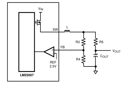
Figure 6. Low Ripple Output Configuration
Page 9
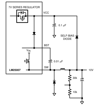
Figure 7. Self Biased Configuration
Over-Voltage Comparator The over-voltage comparator is provided to protect the output from overvoltage conditions due to sudden input line voltage changes or output loading changes. The over-voltage comparator monitors the FB pin versus an internal 2.875V reference. If the voltage at FB rises above 2.875V the comparator immediately terminates the buck switch on-time pulse.
ON Time generator and Shutdown The on-time of the LM25007 is set inversely proportional to the input voltage by an external resistor connected between RON/SD and VIN. The RON/SD terminal is a low impedance input biased at approximately 1.5V. The current through the resistor and into the RON/SD pin is approximately proportional to Vin and used internally to control the on-timer. This scheme of input voltage feed-forward hysteretic operation achieves nearly constant operational frequency over varying line and load conditions. The on-time equation for the LM25007 is : Ton = 1.42 x 10⁻¹⁰ x RON / VIN
(4)
The RON/SD pin of the LM25007 also provides a shutdown function which disables the regulator and significantly decreases quiescent power dissipation. By pulling the pin below 0.7V activates the low power shutdown mode. The VIN quiescent current in the shutdown mode is approximately 100µA internal to the LM25007 plus the current in the RON resistor. See Figure 8.
Page 10
| Column 1 | Column 2 |
|---|---|
| VIN VIN | 7V SERIES REGULATOR ON TIMER VIN START RON COMPLETE LM25007 |
| RON RON/SD STOP RUN |
Figure 8. Shutdown Implementation
Current Limit The LM25007 contains an intelligent current limit off-timer intended to reduce the foldback characteristic inherent with fixed off-time over-current protection. If the current in the Buck switch exceeds 725mA the present cycle on- time is immediately terminated (cycle by cycle current limit). Following the termination of the cycle a nonresetable current limit off timer is initiated. The duration of the off time is a function of the external resistor (RCL) and the FB pin voltage. When the FB pin voltage equals zero, the current limit off-time is internally preset to 17µs. This condition occurs in short circuit operation when a maximum amount of off-time is required.
In cases of overload (not complete short circuit) the current limit off-time is reduced as a function of the output voltage (measured at the FB pin). Reducing the off-time with smaller overloads reduces the amount of foldback and also reduces the initial start-up time. The current limit off time for a given FB pin voltage and RCL resistor can be calculated by the following equation: Toff = 10-5 / (0.59 + (VFB / 7.22 x 10⁻⁶ x RCL))
(5)
Applications utilizing low resistance inductors and/or a low voltage drop rectifier may require special evaluation at high line, short circuit conditions. In this special case the preset 17µs (FB = 0V) off-time may be insufficient to balance the inductor volt\*time product. Additional inductor resistance, output resistance or a larger voltage drop rectifier may be necessary to balance the inductor cycle volt\*time product and limit the short circuit current.
N - Channel Buck Switch and Driver The LM25007 integrates an N-Channel Buck switch and associated floating high voltage gate driver. The gate driver circuit works in conjunction with an external bootstrap capacitor and an internal high voltage diode. The bootstrap capacitor is charged by VCC through the internal high voltage diode. A 0.01uF ceramic capacitor connected between the BST pin and SW pin is recommended. During each cycle when the Buck switch turns off, the SW pin is approximately 0V. When the SW pin voltage is low, the bootstrap capacitor is charged from Vcc through the internal diode. The minimum off timer, set to 300ns, ensures that there will be a minimum interval every cycle to recharge the bootstrap capacitor.
An external re-circulating diode from the SW pin to ground is necessary to carry the inductor current after the internal Buck switch turns off. This external diode must be of the Ultra-fast or Schottky type to reduce turn-on losses and current over-shoot. The reverse voltage rating of the re-circulating diode must be greater than the maximum line input voltage.
Page 11
Thermal Protection
Internal Thermal Shutdown circuitry is provided to protect the integrated circuit in the event the maximum junction
temperature is exceeded. When thermal protection is activated, typically at 165 degrees Celsius, the controller is
forced into a low power reset state, disabling the output driver. This feature is provided to prevent catastrophic
failures from accidental device overheating.
Minimum Load Current
A minimum load current of 1 mA is required to maintain proper operation. If the load current falls below that level,
the bootstrap capacitor may discharge during the long off-time, and the circuitwill either shutdown, or cycle on
and off at a low frequency. If the load current is expected to drop below 1 mA in the application, the feedback
resistors should be chosen low enough in value so they provide the minimum required current at nominal Vout.
10V, 400mA Demo Board Bill of Materials
See Typical Application Circuit and Block Diagram
Table 1. Bill of Materials
| ITEM | PART NUMBER | DESCRIPTION | VALUE |
|---|---|---|---|
| C1 | C4532X7R2A105M | CAPACITOR, CER, TDK | 1µ, 100V |
| C2 | C4532X7R1E156M | CAPACITOR, CER, TDK | 15µ, 25V |
| C3 | C1206C104K5RAC | CAPACITOR, CER, KEMET | 0.1µ, 50V |
| C4 | C1206C103K5RAC | CAPACITOR, CER, KEMET | 0.01µ, 50V |
| C5 | C3216X7R2A104KT | CAPACITOR, CER, TDK | 0.1µ, 100V |
| D1 | MURA110T3 | DIODE, 100V, ON SEMI | |
| L1 | SLF7045T-101MR60-1 | BUCK INDUCTOR, TDK | 100µH |
| R1 | CRCW12062003F | RESISTOR | 200K |
| R2 | CRCW12061003F | RESISTOR | 100K |
| R3 | CRCW12063011F | RESISTOR | 3.01K |
| R4 | CRCW12061001F | RESISTOR | 1K |
| R5 | CRCW12061R00F | RESISTOR | 1 |
| U1 | LM25007 | REGULATOR, TI |
Page 12
REVISION HISTORY
Changes from Revision B (February 2013) to Revision C
Page
- Changed layout of National Data Sheet to TI format .......................................................................................................... 11
Page 13
PACKAGE OPTION ADDENDUM
23-May-2025
PACKAGING INFORMATION
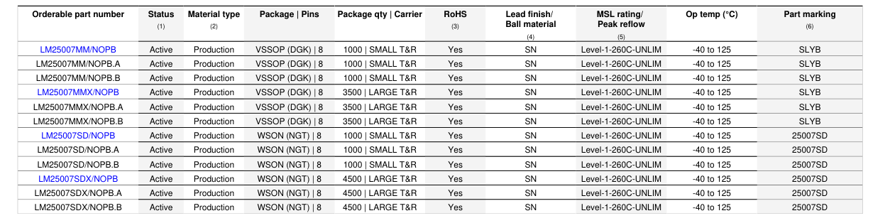
(1) Status: For more details on status, see our product life cycle.
(2) Material type: When designated, preproduction parts are prototypes/experimental devices, and are not yet approved or released for full production. Testing and final process, including without limitation quality assurance, reliability performance testing, and/or process qualification, may not yet be complete, and this item is subject to further changes or possible discontinuation. If available for ordering, purchases will be subject to an additional waiver at checkout, and are intended for early internal evaluation purposes only. These items are sold without warranties of any kind.
(3) RoHS values: Yes, No, RoHS Exempt. See the TI RoHS Statement for additional information and value definition.
(4) Lead finish/Ball material: Parts may have multiple material finish options. Finish options are separated by a vertical ruled line. Lead finish/Ball material values may wrap to two lines if the finish value exceeds the maximum column width.
(5) MSL rating/Peak reflow: The moisture sensitivity level ratings and peak solder (reflow) temperatures. In the event that a part has multiple moisture sensitivity ratings, only the lowest level per JEDEC standards is shown. Refer to the shipping label for the actual reflow temperature that will be used to mount the part to the printed circuit board.
(6) Part marking: There may be an additional marking, which relates to the logo, the lot trace code information, or the environmental category of the part.
Multiple part markings will be inside parentheses. Only one part marking contained in parentheses and separated by a "~" will appear on a part. If a line is indented then it is a continuation of the previous line and the two combined represent the entire part marking for that device.
Addendum-Page 1
Page 14
PACKAGE OPTION ADDENDUM
23-May-2025
Important Information and Disclaimer:The information provided on this page represents TI's knowledge and belief as of the date that it is provided. TI bases its knowledge and belief on information provided by third parties, and makes no representation or warranty as to the accuracy of such information. Efforts are underway to better integrate information from third parties. TI has taken and continues to take reasonable steps to provide representative and accurate information but may not have conducted destructive testing or chemical analysis on incoming materials and chemicals. TI and TI suppliers consider certain information to be proprietary, and thus CAS numbers
and other limited information may not be available for release.
In no event shall TI's liability arising out of such information exceed the total purchase price of the TI part(s) at issue in this document sold by TI to Customer on an annual basis.
Addendum-Page 2
Page 15
TAPE AND REEL INFORMATION
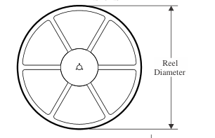
REEL DIMENSIONS
PACKAGE MATERIALS INFORMATION
25-Sep-2024
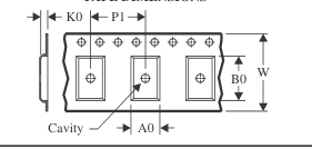
TAPE DIMENSIONS
| Column 1 | Column 2 |
|---|---|
| A0 | Dimension designed to accommodate the component width |
| B0 | Dimension designed to accommodate the component length |
| K0 | Dimension designed to accommodate the component thickness |
| W | Overall width of the carrier tape |
| P1 | Pitch between successive cavity centers |
Reel Width (W1)
QUADRANT ASSIGNMENTS FOR PIN 1 ORIENTATION IN TAPE
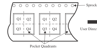
Sprocket Holes
User Direction of Feed
\*All dimensions are nominal
| Device | Package Type | Package Drawing | Pins | SPQ | Reel Diameter (mm) | Reel Width W1 (mm) | A0 (mm) | B0 (mm) | K0 (mm) | P1 (mm) | W (mm) | Pin1 Quadrant |
|---|---|---|---|---|---|---|---|---|---|---|---|---|
| LM25007MM/NOPB | VSSOP | DGK | 8 | 1000 | 178.0 | 12.4 | 5.3 | 3.4 | 1.4 | 8.0 | 12.0 | Q1 |
| LM25007MMX/NOPB | VSSOP | DGK | 8 | 3500 | 330.0 | 12.4 | 5.3 | 3.4 | 1.4 | 8.0 | 12.0 | Q1 |
| LM25007SD/NOPB | WSON | NGT | 8 | 1000 | 178.0 | 12.4 | 4.3 | 4.3 | 1.3 | 8.0 | 12.0 | Q1 |
| LM25007SDX/NOPB | WSON | NGT | 8 | 4500 | 330.0 | 12.4 | 4.3 | 4.3 | 1.3 | 8.0 | 12.0 | Q1 |
Pack Materials-Page 1
Page 16
PACKAGE MATERIALS INFORMATION
25-Sep-2024
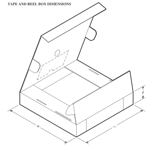
\*All dimensions are nominal
| Device | Package Type | Package Drawing | Pins | SPQ | Length (mm) | Width (mm) | Height (mm) |
|---|---|---|---|---|---|---|---|
| LM25007MM/NOPB | VSSOP | DGK | 8 | 1000 | 210.0 | 185.0 | 35.0 |
| LM25007MMX/NOPB | VSSOP | DGK | 8 | 3500 | 367.0 | 367.0 | 35.0 |
| LM25007SD/NOPB | WSON | NGT | 8 | 1000 | 210.0 | 185.0 | 35.0 |
| LM25007SDX/NOPB | WSON | NGT | 8 | 4500 | 367.0 | 367.0 | 35.0 |
Pack Materials-Page 2
Page 17
PACKAGE OUTLINE
DGK0008A
VSSOP - 1.1 mm max height
SMALL OUTLINE PACKAGE
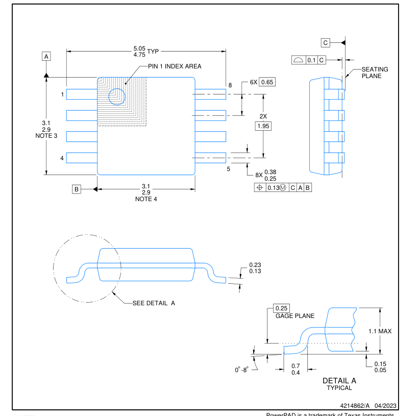
PowerPAD is a trademark of Texas Instruments.
NOTES:
- All linear dimensions are in millimeters. Any dimensions in parenthesis are for reference only. Dimensioning and tolerancing per ASME Y14.5M. 2. This drawing is subject to change without notice. 3. This dimension does not include mold flash, protrusions, or gate burrs. Mold flash, protrusions, or gate burrs shall not exceed 0.15 mm per side. 4. This dimension does not include interlead flash. Interlead flash shall not exceed 0.25 mm per side. 5. Reference JEDEC registration MO-187.
Page 18
EXAMPLE BOARD LAYOUT
DGK0008A
TM
VSSOP - 1.1 mm max height
SMALL OUTLINE PACKAGE
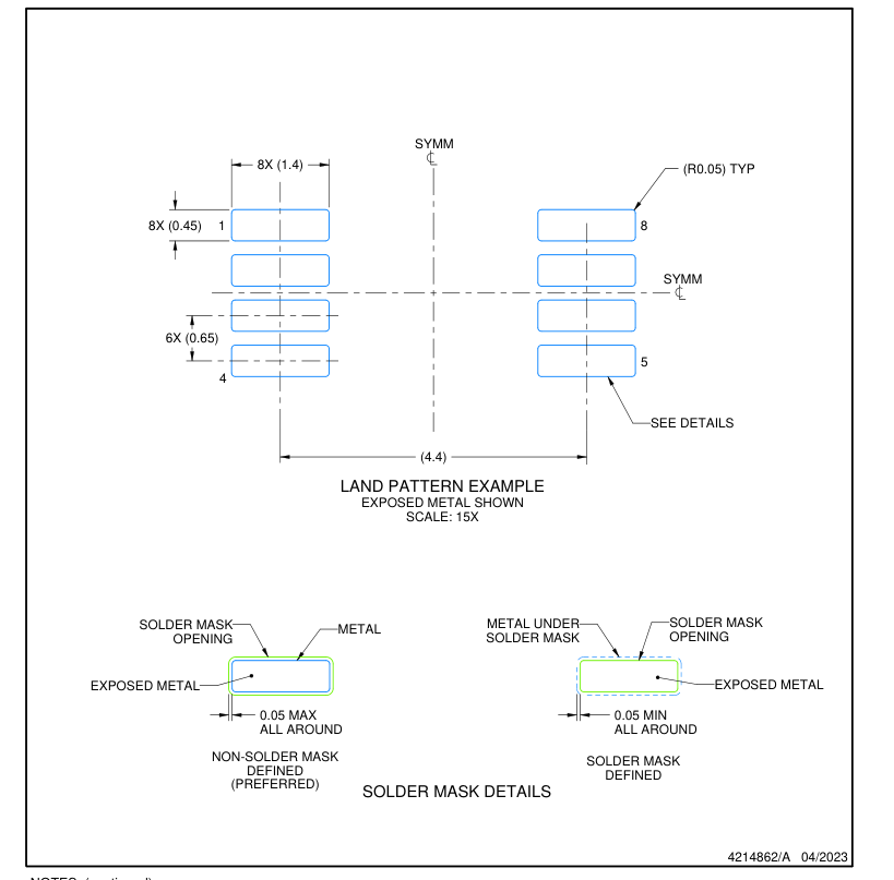
NOTES: (continued)
- Publication IPC-7351 may have alternate designs. 7. Solder mask tolerances between and around signal pads can vary based on board fabrication site. 8. Vias are optional depending on application, refer to device data sheet. If any vias are implemented, refer to their locations shown on this view. It is recommended that vias under paste be filled, plugged or tented. 9. Size of metal pad may vary due to creepage requirement.
Page 19
EXAMPLE STENCIL DESIGN
DGK0008A
TM
VSSOP - 1.1 mm max height
SMALL OUTLINE PACKAGE
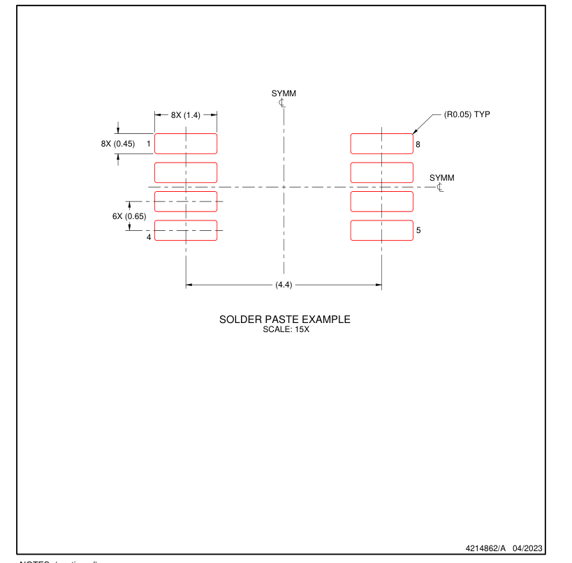
NOTES: (continued)
- Laser cutting apertures with trapezoidal walls and rounded corners may offer better paste release. IPC-7525 may have alternate design recommendations. 12. Board assembly site may have different recommendations for stencil design.
Page 20
PACKAGE OUTLINE
NGT0008A
WSON - 0.8 mm max height
PLASTIC SMALL OUTLINE - NO LEAD
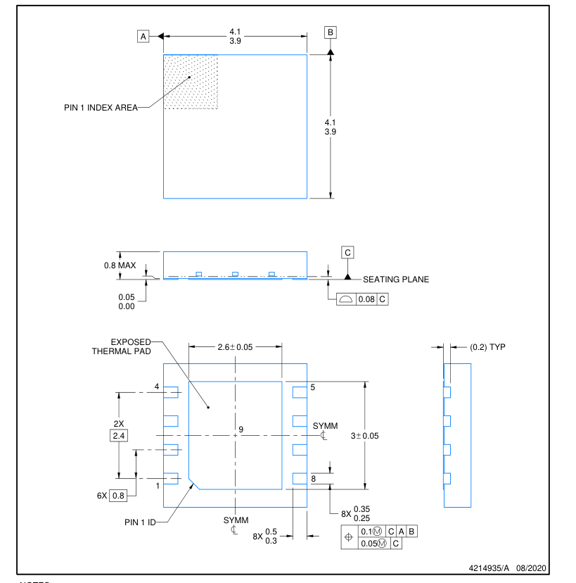
NOTES:
- All linear dimensions are in millimeters. Any dimensions in parenthesis are for reference only. Dimensioning and tolerancing per ASME Y14.5M. 2. This drawing is subject to change without notice. 3. The package thermal pad must be soldered to the printed circuit board for thermal and mechanical performance.
Page 21
EXAMPLE BOARD LAYOUT
NGT0008A
WSON - 0.8 mm max height
PLASTIC SMALL OUTLINE - NO LEAD
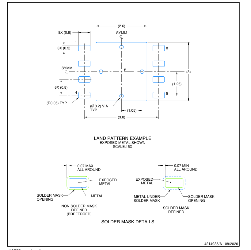
NOTES: (continued)
- This package is designed to be soldered to a thermal pad on the board. For more information, see Texas Instruments literature number SLUA271 (www.ti.com/lit/slua271). 5. Vias are optional depending on application, refer to device data sheet. If any vias are implemented, refer to their locations shown on this view. It is recommended that vias under paste be filled, plugged or tented.
Page 22
EXAMPLE STENCIL DESIGN
NGT0008A
WSON - 0.8 mm max height
PLASTIC SMALL OUTLINE - NO LEAD
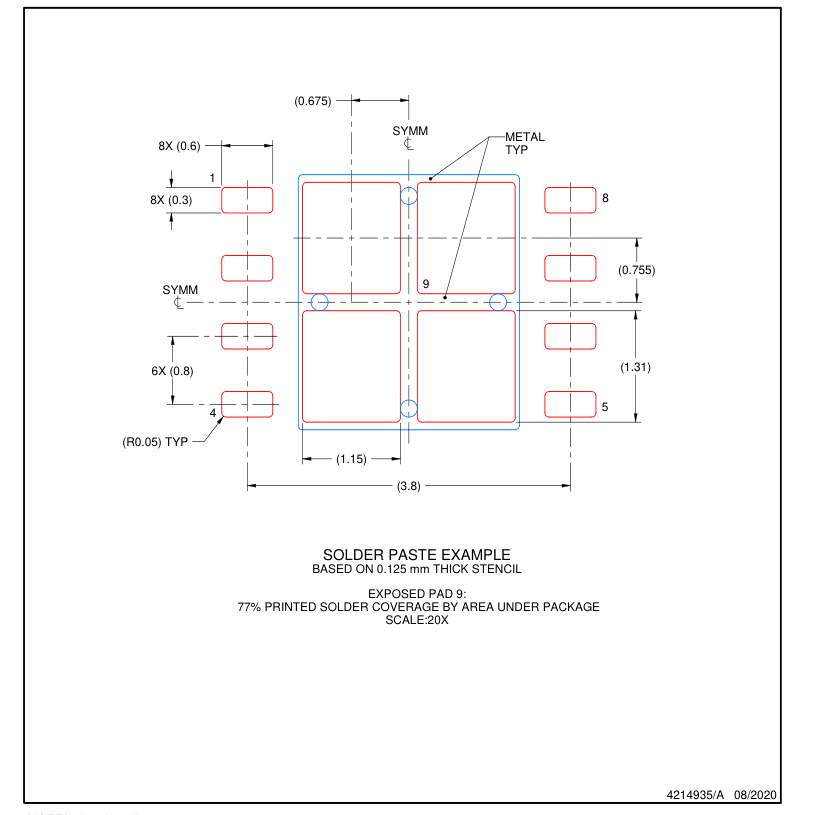
NOTES: (continued)
- Laser cutting apertures with trapezoidal walls and rounded corners may offer better paste release. IPC-7525 may have alternate design recommendations.
Page 23
IMPORTANT NOTICE AND DISCLAIMER
TI PROVIDES TECHNICAL AND RELIABILITY DATA (INCLUDING DATA SHEETS), DESIGN RESOURCES (INCLUDING REFERENCE DESIGNS), APPLICATION OR OTHER DESIGN ADVICE, WEB TOOLS, SAFETY INFORMATION, AND OTHER RESOURCES “AS IS” AND WITH ALL FAULTS, AND DISCLAIMS ALL WARRANTIES, EXPRESS AND IMPLIED, INCLUDING WITHOUT LIMITATION ANY IMPLIED WARRANTIES OF MERCHANTABILITY, FITNESS FOR A PARTICULAR PURPOSE OR NON-INFRINGEMENT OF THIRD PARTY INTELLECTUAL PROPERTY RIGHTS. These resources are intended for skilled developers designing with TI products. You are solely responsible for (1) selecting the appropriate TI products for your application, (2) designing, validating and testing your application, and (3) ensuring your application meets applicable
standards, and any other safety, security, regulatory or other requirements. These resources are subject to change without notice. TI grants you permission to use these resources only for development of an application that uses the TI products described in the resource. Other reproduction and display of these resources is prohibited. No license is granted to any other TI intellectual property right or to any third party intellectual property right. TI disclaims responsibility for, and you will fully indemnify TI and its representatives against, any claims, damages, costs, losses, and liabilities arising out of your use of these resources. TI’s products are provided subject to TI’s Terms of Sale or other applicable terms available either on ti.com or provided in conjunction with
such TI products. TI’s provision of these resources does not expand or otherwise alter TI’s applicable warranties or warranty disclaimers for TI products. TI objects to and rejects any additional or different terms you may have proposed. IMPORTANT NOTICE
Mailing Address: Texas Instruments, Post Office Box 655303, Dallas, Texas 75265
Copyright © 2025, Texas Instruments Incorporated