


 Download PDF
DATASHEET SEARCH SITE
Document overview
- PDF pages: 8
Technical content
Page 1
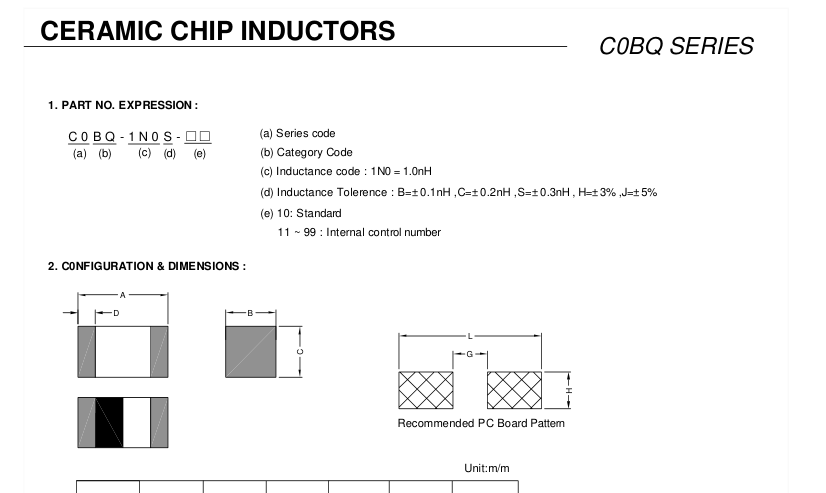
| B | C | D | L | G | H |
| 0.03 0.30± 0.03 | 0.30± 0.03 | 0.10± 0.05 | 0.80 Ref. | 0.20~0.30 | 0.25~0.40 |
A
0.60± 0.03
Page 2

| Part Number | Inductance (nH) | Tolerance | Test Frequency ( MHz ) | Q Min | Q(Typ.) Frequency(Hz) | Rated Current (mA) Max | DCR ( Ω ) Max. | ||||
|---|---|---|---|---|---|---|---|---|---|---|---|
| 500M | 800M | 1.8G | 2.0G | 2.4G | |||||||
| C0BQ-0N6□-10 | 0.6 | B,C,S | 500 | 14 | >35 | >47 | >75 | >80 | >88 | 900 | 0.06 |
| C0BQ-0N7□-10 | 0.7 | B,C,S | 500 | 14 | >35 | >47 | >75 | >80 | >88 | 900 | 0.06 |
| C0BQ-0N8□-10 | 0.8 | B,C,S | 500 | 14 | >35 | >47 | >75 | >80 | >88 | 900 | 0.06 |
| C0BQ-0N9□-10 | 0.9 | B,C,S | 500 | 14 | >35 | >47 | >75 | >80 | >88 | 900 | 0.06 |
| C0BQ-1N0□-10 | 1.0 | B,C,S | 500 | 14 | >35 | >47 | >75 | >80 | >88 | 850 | 0.07 |
| C0BQ-1N1□-10 | 1.1 | B,C,S | 500 | 14 | >35 | >47 | >75 | >80 | >88 | 850 | 0.07 |
| C0BQ-1N2□-10 | 1.2 | B,C,S | 500 | 14 | 35 | 47 | 75 | 80 | 88 | 800 | 0.08 |
| C0BQ-1N3□-10 | 1.3 | B,C,S | 500 | 14 | 32 | 43 | 70 | 74 | 82 | 760 | 0.09 |
| C0BQ-1N4□-10 | 1.4 | B,C,S | 500 | 14 | 29 | 39 | 63 | 67 | 75 | 640 | 0.12 |
| C0BQ-1N5□-10 | 1.5 | B,C,S | 500 | 14 | 27 | 36 | 59 | 62 | 69 | 600 | 0.15 |
| C0BQ-1N6□-10 | 1.6 | B,C,S | 500 | 14 | 25 | 33 | 54 | 57 | 63 | 510 | 0.19 |
| C0BQ-1N7□-10 | 1.7 | B,C,S | 500 | 14 | 25 | 32 | 52 | 54 | 61 | 680 | 0.11 |
| C0BQ-1N8□-10 | 1.8 | B,C,S | 500 | 14 | 25 | 32 | 51 | 53 | 59 | 640 | 0.12 |
| C0BQ-1N9□-10 | 1.9 | B,C,S | 500 | 14 | 24 | 31 | 50 | 53 | 58 | 620 | 0.13 |
| C0BQ-2N0□-10 | 2.0 | B,C,S | 500 | 14 | 24 | 31 | 50 | 53 | 58 | 600 | 0.15 |
| C0BQ-2N1□-10 | 2.1 | B,C,S | 500 | 14 | 24 | 31 | 50 | 53 | 58 | 550 | 0.16 |
| C0BQ-2N2□-10 | 2.2 | B,C,S | 500 | 14 | 24 | 31 | 50 | 53 | 58 | 500 | 0.20 |
| C0BQ-2N3□-10 | 2.3 | B,C,S | 500 | 14 | 24 | 31 | 49 | 52 | 58 | 460 | 0.24 |
| C0BQ-2N4□-10 | 2.4 | B,C,S | 500 | 14 | 22 | 28 | 45 | 48 | 53 | 430 | 0.26 |
| C0BQ-2N5□-10 | 2.5 | B,C,S | 500 | 14 | 22 | 29 | 46 | 49 | 54 | 415 | 0.28 |
| C0BQ-2N6□-10 | 2.6 | B,C,S | 500 | 14 | 21 | 27 | 44 | 46 | 51 | 405 | 0.30 |
| C0BQ-2N7□-10 | 2.7 | B,C,S | 500 | 14 | 20 | 26 | 41 | 43 | 48 | 400 | 0.32 |
| C0BQ-2N8□-10 | 2.8 | B,C,S | 500 | 14 | 20 | 26 | 41 | 43 | 47 | 500 | 0.20 |
| C0BQ-2N9□-10 | 2.9 | B,C,S | 500 | 14 | 20 | 26 | 41 | 43 | 47 | 480 | 0.22 |
| C0BQ-3N0□-10 | 3.0 | B,C,S | 500 | 14 | 20 | 26 | 41 | 43 | 47 | 460 | 0.24 |
| C0BQ-3N1□-10 | 3.1 | B,C,S | 500 | 14 | 20 | 26 | 41 | 43 | 47 | 450 | 0.25 |
| C0BQ-3N2□-10 | 3.2 | B,C,S | 500 | 14 | 20 | 26 | 40 | 43 | 47 | 415 | 0.28 |
| C0BQ-3N3□-10 | 3.3 | B,C,S | 500 | 14 | 20 | 26 | 40 | 43 | 47 | 415 | 0.28 |
| C0BQ-3N4□-10 | 3.4 | B,C,S | 500 | 14 | 20 | 25 | 40 | 43 | 47 | 410 | 0.29 |
| C0BQ-3N5□-10 | 3.5 | B,C,S | 500 | 14 | 20 | 25 | 40 | 42 | 46 | 405 | 0.30 |
| C0BQ-3N6□-10 | 3.6 | B,C,S | 500 | 14 | 19 | 25 | 40 | 42 | 46 | 400 | 0.32 |
| C0BQ-3N7□-10 | 3.7 | B,C,S | 500 | 14 | 19 | 25 | 40 | 42 | 46 | 370 | 0.36 |
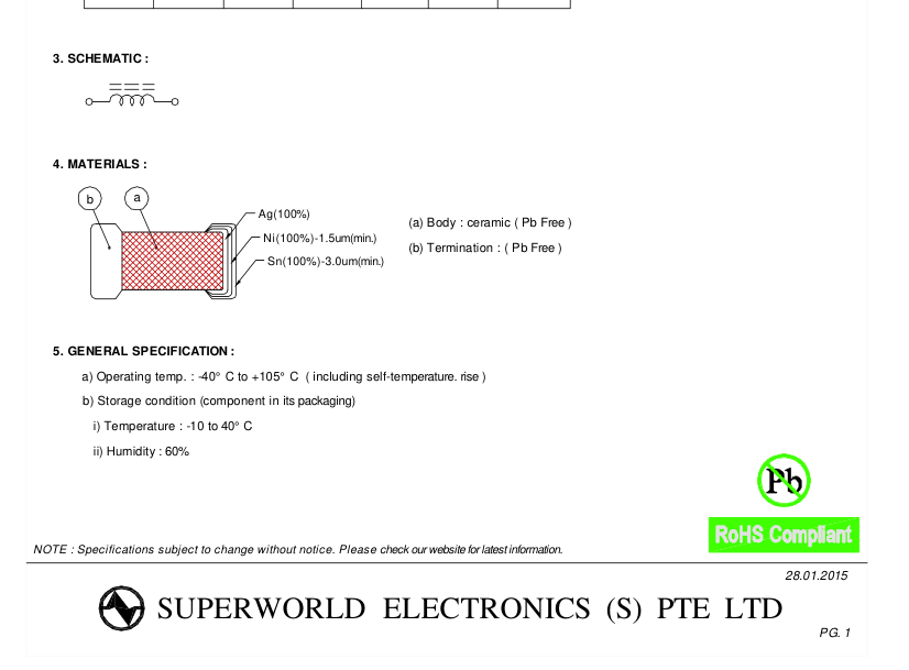
| C0BQ-3N8□-10 | 3.8 | B,C,S | 500 | 14 | 19 | 25 | 39 | 41 | 45 | 355 | 0.40 |
( MHz ) Min.
10000
10000
10000
10000
10000
10000
10000
10000
10000
10000
10000
10000
10000
10000
10000
10000
10000
10000
10000
10000
10000
10000
9500
9300
9100
8900
8700
8600
8400
8200
8100
8000
7800
Page 3

| Part Number | Inductance (nH) | Tolerance | Test Frequency ( MHz ) | Q Min | Q(Typ.) Frequency(Hz) | Rated Current (mA) Max | DCR ( Ω ) Max. | ||||
|---|---|---|---|---|---|---|---|---|---|---|---|
| 500M | 800M | 1.8G | 2.0G | 2.4G | |||||||
| C0BQ-4N0□-10 | 4.0 | B,C,S | 500 | 14 | 18 | 25 | 39 | 41 | 45 | 335 | 0.44 |
| C0BQ-4N1□-10 | 4.1 | B,C,S | 500 | 14 | 19 | 25 | 39 | 41 | 45 | 320 | 0.48 |
| C0BQ-4N2□-10 | 4.2 | B,C,S | 500 | 14 | 18 | 24 | 37 | 39 | 43 | 320 | 0.48 |
| C0BQ-4N3□-10 | 4.3 | C,S | 500 | 14 | 18 | 24 | 37 | 39 | 43 | 320 | 0.48 |
| C0BQ-4N6□-10 | 4.6 | C,S | 500 | 14 | 18 | 24 | 37 | 39 | 42 | 360 | 0.39 |
| C0BQ-4N7□-10 | 4.7 | C,S | 500 | 14 | 19 | 24 | 37 | 39 | 42 | 350 | 0.42 |
| C0BQ-5N0□-10 | 5.0 | C,S | 500 | 14 | 19 | 24 | 37 | 39 | 42 | 335 | 0.44 |
| C0BQ-5N1□-10 | 5.1 | C,S | 500 | 14 | 19 | 24 | 37 | 39 | 42 | 330 | 0.45 |
| C0BQ-5N4□-10 | 5.4 | C,S | 500 | 14 | 18 | 24 | 36 | 38 | 42 | 315 | 0.49 |
| C0BQ-5N6□-10 | 5.6 | C,S | 500 | 14 | 18 | 24 | 36 | 37 | 41 | 325 | 0.47 |
| C0BQ-5N9□-10 | 5.9 | C,S | 500 | 14 | 18 | 23 | 35 | 36 | 39 | 325 | 0.47 |
| C0BQ-6N2□-10 | 6.2 | C,S | 500 | 14 | 18 | 23 | 35 | 36 | 39 | 305 | 0.52 |
| C0BQ-6N5□-10 | 6.5 | C,S | 500 | 14 | 18 | 23 | 35 | 36 | 39 | 305 | 0.52 |
| C0BQ-6N8□-10 | 6.8 | H,J | 500 | 14 | 18 | 23 | 35 | 36 | 39 | 305 | 0.55 |
| C0BQ-7N1□-10 | 7.1 | H,J | 500 | 14 | 18 | 23 | 35 | 36 | 39 | 305 | 0.55 |
| C0BQ-7N5□-10 | 7.5 | H,J | 500 | 14 | 18 | 23 | 34 | 35 | 38 | 305 | 0.55 |
| C0BQ-7N8□-10 | 7.8 | H,J | 500 | 14 | 17 | 22 | 33 | 34 | 36 | 310 | 0.51 |
| C0BQ-8N2□-10 | 8.2 | H,J | 500 | 14 | 17 | 22 | 33 | 34 | 36 | 290 | 0.57 |
| C0BQ-8N5□-10 | 8.5 | H,J | 500 | 14 | 17 | 22 | 33 | 34 | 36 | 290 | 0.57 |
| C0BQ-9N1□-10 | 9.1 | H,J | 500 | 14 | 17 | 22 | 33 | 34 | 36 | 270 | 0.65 |
| C0BQ-9N4□-10 | 9.4 | H,J | 500 | 14 | 17 | 22 | 33 | 34 | 36 | 250 | 0.73 |
| C0BQ-10N□-10 | 10.0 | H,J | 500 | 14 | 17 | 22 | 33 | 34 | 36 | 230 | 0.85 |
| C0BQ-12N□-10 | 12.0 | H,J | 500 | 14 | 17 | 22 | 31 | 32 | 33 | 230 | 0.85 |
| C0BQ-15N□-10 | 15.0 | H,J | 500 | 14 | 17 | 21 | 28 | 29 | 29 | 220 | 0.89 |
| C0BQ-18N□-10 | 18.0 | H,J | 500 | 14 | 16 | 21 | 26 | 26 | 25 | 205 | 1.05 |
| C0BQ-22N□-10 | 22.0 | H,J | 500 | 14 | 16 | 21 | 26 | 26 | 24 | 190 | 1.29 |
( MHz ) Min.
7600
7500
7300
6500
6500
6400
6200
6100
5900
5500
5500
5100
5100
4800
4800
4600
4600
4300
4300
4000
4000
3800
3300
2600
2300
1900
Page 4
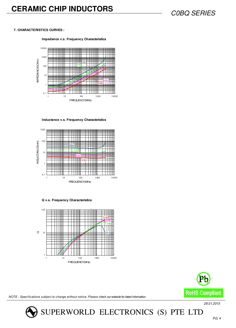
Page 5
8. SOLDERING AND MOUNTING :
8-1. Recommended PC Board Pattern
Unit:m/m
L
| L | G | H |
| 0.80 | 0.20~0.30 | 0.25~0.40 |
G
PC board should be designed so that products are not sufficient under mechanical stress as warping the board. Products shall be positioned in the sideway direction against the mechanical stress to prevent failure.
8-2. Soldering
Mildly activated rosin fluxes are preferred. The terminations are suitable for re-flow soldering systems. If hand soldering cannot be avoided, the preferred technique is the utilization of hot air soldering tools. Note. If wave soldering is used ,there will be some risk. Re-flow soldering temperatures below 240 degrees, there will be non-wetting risk
8-2.1 Lead Free Solder Re-flow : Recommended temperature profiles for re-flow soldering in Figure 1.
8-2.2 Soldering Iron (Figure 2) :
Products attachment with soldering iron is discouraged due to the inherent process Control limitations. In the event that a soldering iron must be employed the following precautions are reCommended. Note : a) Preheat circuit and products to 150° C. b) 350° C tip temperature (max) c) Never Contact the ceramic with the iron tip
Preheating Soldering Natural Cooling 20~40s
TP(260° C/40s max.)
217 200 150
60~150s
60~180s 480s max. 25
Time(sec.)
Figure 1. Re-flow Soldering : 3 times max
d) 1.0mm tip diameter (max) e) Use a 20 watt soldering iron with tip diameter of 1.0mm f) Limit soldering time to 4 ~ 5 secs.
Preheating Soldering Natural Cooling Within 4~5s
350
150
Gradual
Over 1min.
C0oling
Figure 2. Hand Soldering : 1 times max
NOTE : Specifications subject to change without notice. Please check our website for latest information.
28.01.2015
SUPERWORLD ELECTRONICS (S) PTE LTD
PG. 5
Page 6
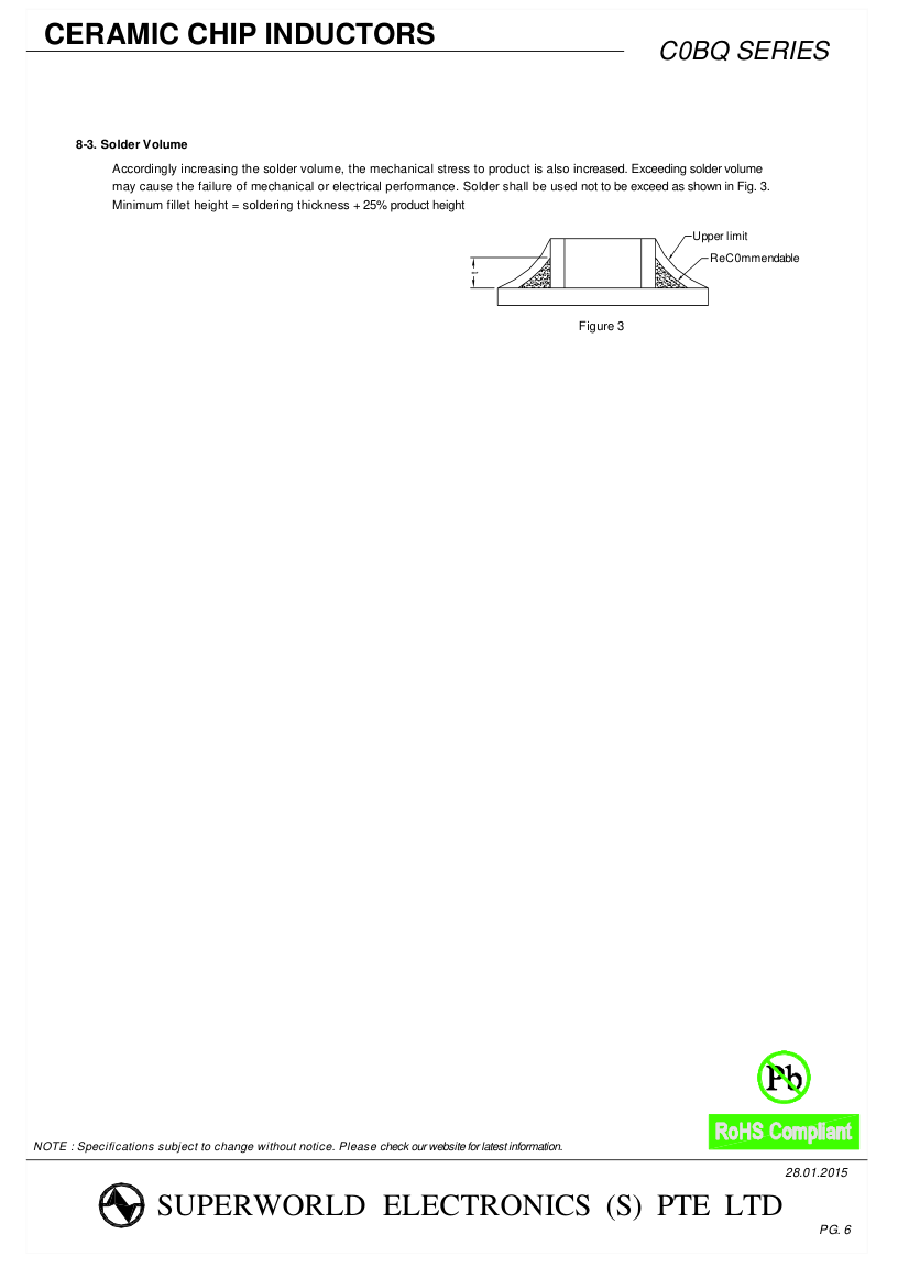
Page 7
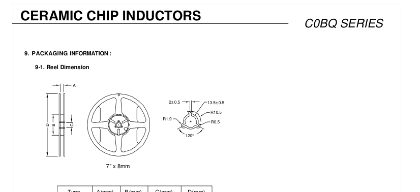
| Type | A(mm) | B(mm) | C(mm) D | (mm) |
|---|---|---|---|---|
| " x 8mm | 9.0±0.5 | 60±2 | 13.52±0.5 17 | 8.0±2.0 |
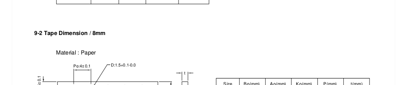
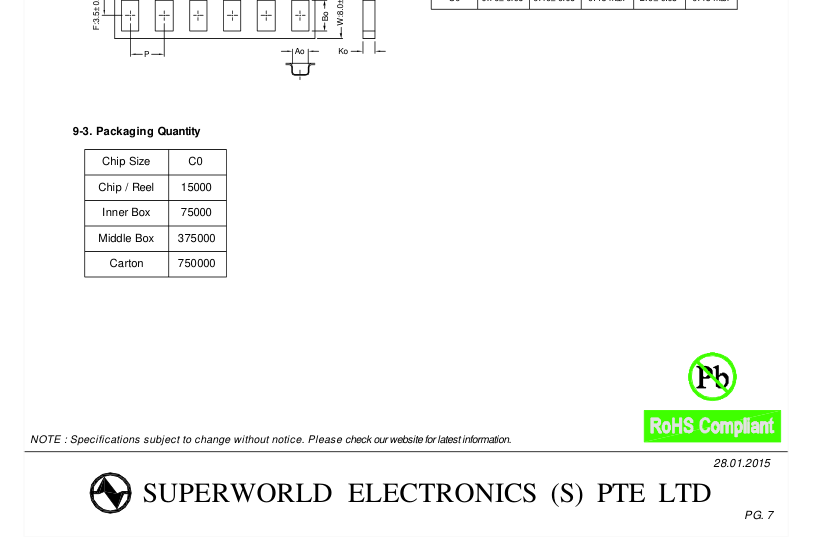
| Size | Bo(mm) | Ao(mm) | Ko(mm) | P(mm) t(mm) |
| C0 | 0.70± 0.06 | 0.40± 0.06 | 0.45 max | 2.0± 0.05 0.45 ma |
Page 8
9-4. Tearing Off Force
F 165° C to 180° C
Top cover tape
Base tape
Application Notice
- Storage Conditions : To maintain the solderabililty of terminal electrodes :
The force for tearing off cover tape is 15 to 60 grams in the arrow direction under the following conditions.
| Room Temp. (° C) | Room Humidity (%) | Room atm Tearin (hPa) (mm |
| 5~35 | 45~85 | 860~1060 3 |
Tearing Speed (mm/min)
300
a) Recommended products should be used within 12 months from the time of delivery. b) The packaging material should be kept where no chlorine or sulfur exists in the air.
- Transportation : a) Products should be handled with care to avoid damage or contamination from perspiration and skin oils. b) The use of tweezers or vacuum pick up is strongly recommended for individual components. c) Bulk handling should ensure that abrasion and mechanical shock are minimized.
NOTE : Specifications subject to change without notice. Please check our website for latest information.
28.01.2015
SUPERWORLD ELECTRONICS (S) PTE LTD
PG. 8