

 Download PDF
BL0200 SANKEN
Document overview
- PDF pages: 26
Technical content
Page 1
High Efficiency
For LED Backlight 2ch LED Driver IC
General Descriptions
BL0200 series are 2ch output LED driver IC for LED backlight, and it can do dimming to 0.02 % by external PWM signal. This IC realizes a high efficiency by the boost convertor control that absorbs variability on VF. The product easily achieves high cost-performance LED drive system with few external components and enhanced protection functions.
Features and Benefit
Boost convertor
- Current-Mode type PWM Control
- PWM frequency is 100 kHz or 200 kHz
- Maximum On Duty is 90 %
LED current control
- Individual PWM Dimming Control
- Analog Dimming
- High contrast ratio is 1 / 5000
- Accuracy of Reg output voltage is ± 1.5 % or ± 2 %
Protection functions
- Enable Function of IC (BL0202B, BL0202C)
- Error Signal Output (BL0200C)
- Overcurrent Protection for Boost Circuit (OCP) ---------------------------------------------- Pulse-by-pulse
- Overcurrent Protection for LED Output (LED_OCP) ---------------------------------------------- Pulse-by-pulse
- Overvoltage Protection (OVP) ----------- Auto restart
- Output Open/Short Protection ------------ Auto restart
- Thermal Shutdown (TSD) ----------------- Auto restart
Typical Application Circuit
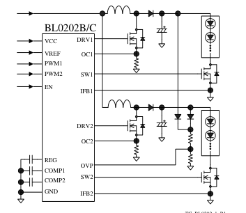
TC_BL0202_1_R1
Package
SOP18
Not to scale
Lineup
| Products | Frequency | V REG Accuracy | Built-in Function |
| BL0202C | 200 kHz | ± 1.5 % | Enable Function of IC |
| BL0202B | 100 kHz | ||
| BL0200C | 200 kHz | ± 2 % | Error Signal Output |
Applications
- LED backlights
- LED lighting etc.
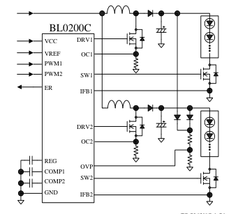
TC_BL0200C_1_R1
Page 2
CONTENTS
Lineup ----------------------------------------------------------------------------------------- 1 Applications ---------------------------------------------------------------------------------- 1 1. Absolute Maximum Ratings --------------------------------------------------------- 3 2. Electrical characteristics ------------------------------------------------------------- 4 3. Functional Block Diagram ----------------------------------------------------------- 6 4. Pin List Table --------------------------------------------------------------------------- 7 5. Typical Application Circuit --------------------------------------------------------- 8 6. Package Diagram ---------------------------------------------------------------------- 9
- Marking Diagram --------------------------------------------------------------------- 9 8. Functional Description -------------------------------------------------------------- 10 8.1 Startup Operation(BL0200C) -------------------------------------------- 10 8.2 Startup Operation(BL0202B, BL0202C) ------------------------------ 11 8.3 Constant Current Control Operation ----------------------------------- 12 8.4 PWM Dimming Function -------------------------------------------------- 13 8.5 Gate Drive --------------------------------------------------------------------- 13 8.6 Error Signal Output Function (BL0200C) ----------------------------- 14 8.7 Protection Function --------------------------------------------------------- 14
- Design Notes --------------------------------------------------------------------------- 18 9.1 Peripheral Components ---------------------------------------------------- 18 9.2 Inductor Design Parameters----------------------------------------------- 18 9.3 PCD Trace Layout and Component Placement ----------------------- 19 10. Reference Design of Power Supply ----------------------------------------------- 21 10.1 BL0202B ----------------------------------------------------------------------- 21 10.2 BL0200C ----------------------------------------------------------------------- 23
OPERATING PRECAUTIONS -------------------------------------------------------- 25
IMPORTANT NOTES ------------------------------------------------------------------- 26
Page 3
1. Absolute Maximum Ratings
The polarity value for current specifies a sink as "+," and a source as "−," referencing the IC. Unless otherwise specified, TA is 25 °C
| Parameter | Symbol | Test Conditions | Pins | Rating | Unit | Notes |
|---|---|---|---|---|---|---|
| REG Pin Source Current | I REG | 1 – 9 | − 1 | mA | ||
| OVP Pin Voltage | V OVP | 2 – 9 | − 0.3 to 5 | V | ||
| PWM1 Pin Voltage | V PWM1 | 3 – 9 | − 0.3 to 5 | V | ||
| IFB1 Pin Clamp Current | I FB1 | Single pulse 5 µs | 5 – 9 | − 10 | mA | |
| OC1 Pin Voltage | V OC1 | 6 – 9 | − 0.3 to 5 | V | ||
| DRV1 Pin Voltage | V DRV1 | 7 – 9 | − 0.3 to V + 0.3 CC | V | ||
| SW1 Pin Voltage | V SW1 | 8 – 9 | − 0.3 to V + 0.3 CC | V | ||
| VCC Pin Voltage | V CC | 10 – 9 | − 0.3 to 20 | V | ||
| SW2 Pin Voltage | V SW2 | 11 – 9 | − 0.3 to V + 0.3 CC | V | ||
| DRV2 Pin Voltage | V DRV2 | 12 – 9 | − 0.3 to V + 0.3 CC | V | ||
| OC2 Pin Voltage | V OC2 | 13 – 9 | − 0.3 to 5 | V | ||
| IFB2 Pin Clamp Current | I FB2 | Single pulse 5 µs | 14 – 9 | − 10 | mA | |
| PWM2 Pin Voltage | V PWM2 | 16 – 9 | − 0.3 to 5 | V | ||
| EN Pin Voltage | V EN | 17 – 9 | − 0.3 to 5 | V | BL0202B BL0202C | |
| ER Pin Voltage | V ER | 17 – 9 | − 0.3 to V REG | V | BL0200C | |
| VREF Pin Voltage | V REF | 18 – 9 | − 0.3 to 5 | V | ||
| Operating Ambient Temperature | T op | − | − 40 to 85 | °C | ||
| Storage Temperature | T stg | − | − 40 to 125 | °C | ||
| Junction Temperature | T j | − | 150 | °C |
Page 4
2. Electrical characteristics
The polarity value for current specifies a sink as "+," and a source as "−," referencing the IC. Unless otherwise specified, TA is 25 °C, VCC = 12 V
| Parameter | Symbol | Test Conditions | Pins | Min. | Typ. | Max. | Unit | Notes |
|---|---|---|---|---|---|---|---|---|
| Start / Stop Operation | ||||||||
| Operation Start Voltage* | V CC(ON) | 10 – 9 | 8.5 | 9.6 | 10.5 | V | ||
| Operation Stop Voltage | V CC(OFF) | 10 – 9 | 7.8 | 8.6 | 9.2 | V | BL0202B BL0202C | |
| 8.0 | 9.1 | 10.0 | BL0200C | |||||
| Circuit Current in Operation | I CC(ON) | 10 – 9 | − | 5.3 | 8.0 | mA | ||
| Circuit Current in Non-Operation | I CC(OFF) | V = 7.5 V CC | 10 – 9 | − | 70 | 200 | µA | |
| REG Pin Output Voltage | V REG | 1 – 9 | 4.925 | 5.000 | 5.075 | V | BL0202B BL0202C | |
| 4.9 | 5.0 | 5.1 | BL0200C | |||||
| Oscillation | ||||||||
| PWM Operation Frequency | f PWM1 f PWM2 | 7 – 9 12 – 9 | 95 | 100 | 105 | kHz | BL0202B | |
| 190 | 200 | 210 | BL0200C BL0202C | |||||
| Maximum ON Duty | D MAX1 D MAX2 | 7 – 9 12 – 9 | 85 | 90 | 95 | % | ||
| Minimum ON Time | t MIN1 t MIN2 | 7 – 9 12 – 9 | 200 | 310 | 400 | ns | ||
| COMP Pin Voltage at Oscillation Start | V COMP1(ON) V COMP2(ON) | 4 – 9 15 – 9 | 0.35 | 0.50 | 0.65 | V | ||
| COMP Pin Voltage at Oscillation Stop | V COMP1(OFF) V COMP2(OFF) | 4 – 9 15 – 9 | 0.10 | 0.25 | 0.40 | V | ||
| VREF / IFB Pin | ||||||||
| VREF Pin Minimum Setting Voltage | V REF(MIN) | V = 0 V REF | 18 – 9 | 0.05 | 0.25 | 0.45 | V | |
| VREF Pin Maximum Setting Voltage | V REF(MAX) | V = 5 V REF | 18 – 9 | 1.75 | 2.00 | 2.35 | V | |
| IFB Pin Voltage at COMP Charge Switching | V IFB1(COMP1) V IFB2(COMP2) | V = 1 V REF | 5 – 9 14 – 9 | 0.55 | 0.60 | 0.65 | V | |
| IFB Pin Overcurrent Protection High Threshold Voltage | V IFB1(OCH) V IFB2(OCH) | 5 – 9 14 – 9 | 3.8 | 4.0 | 4.2 | V | ||
| IFB Pin Overcurrent Protection Low Threshold Voltage | V IFB1(OCL) V IFB2(OCL) | V = 1 V REF | 5 – 9 14 – 9 | 1.9 | 2.0 | 2.1 | V | |
| IFB Pin Overcurrent Protection Release Threshold Voltage | V IFB1(OCL-OFF) V IFB2(OCL-OFF) | V = 1 V REF | 5 – 9 14 – 9 | 1.5 | 1.6 | 1.7 | V | |
| IFB Pin Voltage at Auto Restart Operation | V IFB1(AR) V IFB2(AR) | V = 1 V REF | 5 – 9 14 – 9 | 0.45 | 0.50 | 0.55 | V | |
| IFB Pin Bias Current | I IFB1(B) I IFB2(B) | V = 5 V IFB1 V = 5 V IFB2 | 5 – 9 14 – 9 | − | − | 1 | µA | |
| Current Detection Threshold Voltage | V IFB1 V IFB2 | V = 1 V REF | 5 – 9 14 – 9 | 0.98 | 1.00 | 1.02 | V | BL0202B BL0202C |
| 0.985 | 1.000 | 1.015 | BL0200C | |||||
| COMP Pin | ||||||||
| COMP Pin Maximum Output Voltage | V COMP1(MAX) V COMP2(MAX) | V = 0.7 V IFB1 V = 0.7 V IFB2 | 4 – 9 15 – 9 | 4.8 | 5.0 | − | V | |
\* VCC(ON) > VCC(OFF)
Page 5
| Parameter | Symbol | Test Conditions | Pins | Min. | Typ. | Max. | Unit | Notes |
|---|---|---|---|---|---|---|---|---|
| COMP Pin Minimum Output Voltage | V COMP1(MIN) V COMP2(MIN) | V = 2.0 V IFB1 V = 2.0 V IFB2 | 4 – 9 15 – 9 | − | 0 | 0.2 | V | |
| Transconductance | gm | − | − | 640 | − | µS | ||
| COMP Pin Source Current | I COMP1(SRC) I COMP2(SRC) | V = 0.7 V IFB1 V = 0.7 V IFB2 | 4 – 9 15 – 9 | −77 | −57 | −37 | µA | |
| COMP Pin Sink Current | I COMP1(SNK) I COMP2(SNK) | V = 1.5 V IFB1 V = 1.5 V IFB2 | 4 – 9 15 – 9 | 37 | 57 | 77 | µA | |
| COMP Pin Charge Current at Startup | I COMP1(S) I COMP2(S) | V = 0 V COMP1 V = 0 V COMP2 | 4 – 9 15 – 9 | −19 | −11 | −3 | µA | |
| COMP Pin Reset Current | I COMP1(R) I COMP2(R) | 4 – 9 15 – 9 | 200 | 360 | 520 | µA | ||
| EN Pin | ||||||||
| Operation Start EN Pin Voltage | V EN(ON) | 17 – 9 | 1.2 | 2.0 | 2.6 | V | BL0202B BL0202C | |
| Operation Stop EN Pin Voltage | V EN(OFF) | 17 – 9 | 0.8 | 1.4 | 1.8 | V | ||
| EN Pin Sink Current | I EN | V = 3 V EN | 17 – 9 | 20 | 55 | 120 | µA | |
| ER Pin | ||||||||
| ER Pin Sink Current during Non-Alarm | I ER | V = 1 V ER | 17 – 9 | 2.5 | 4.4 | 6.3 | mA | BL0200C |
| Boost Parts Overcurrent Protection (OCP) | ||||||||
| OC Pin Overcurrent Protection Threshold Voltage | V OCP1 V OCP2 | V COMP1 = V COMP2 = 4.5 V | 6 – 9 13 – 9 | 0.57 | 0.60 | 0.63 | V | |
| Overvoltage Protection (OVP) | ||||||||
| OVP Pin Overvoltage Protection Threshold Voltage | V OVP | 2 – 9 | 2.85 | 3.00 | 3.15 | V | ||
| OVP Pin OVP Release Threshold Voltage | V OVP(OFF) | 2 – 9 | 2.60 | 2.75 | 2.90 | V | ||
| PWM Pin | ||||||||
| PWM Pin ON Threshold Voltage | V PWM1(ON) V PWM2(ON) | 3 – 9 16 – 9 | 1.4 | 1.5 | 1.6 | V | ||
| PWM Pin OFF Threshold Voltage | V PWM1(OFF) V PWM2(OFF) | 3 – 9 16 – 9 | 0.9 | 1.0 | 1.1 | V | ||
| PWM Pin Impedance | R PWM1 R PWM2 | 3 – 9 16 – 9 | 100 | 200 | 300 | kΩ | ||
| SW / DRV Pin | ||||||||
| SW Pin Source Current | I SW1(SRC) I SW2(SRC) | 8 – 9 11 – 9 | − | −85 | − | mA | ||
| SW Pin Sink Current | I SW1(SNK) I SW2(SNK) | 8 – 9 11 – 9 | − | 220 | − | mA | ||
| DRV Pin Source Current | I DRV1(SRC) I DRV2(SRC) | 7 – 9 12 – 9 | − | −0.36 | − | A | ||
| DRV Pin Sink Current | I DRV1(SNK) I DRV2(SNK) | 7 – 9 12 – 9 | − | 0.85 | − | A | ||
| Thermal Shutdown Protection (TSD) | ||||||||
| Thermal Shutdown Activating Temperature | T j(TSD) | − | 125 | − | − | °C | ||
| Hysteresis Temperature of TSD | T j(TSD)HYS | − | − | 65 | − | °C | ||
| Thermal Resistance | ||||||||
| Thermal Resistance from Junction to Ambient | θ j-A | − | − | − | 95 | °C/W | ||
Page 6
3. Functional Block Diagram
BL0202B, BL0202C
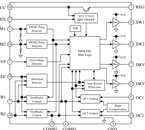
VCC
PWM1
PWM2
OVP
VREF
IFB1
IFB2
BD_BL202_R1
BL0200C
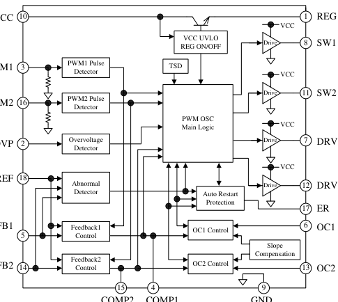
VCC
PWM1
PWM2
OVP
VREF
IFB1
IFB2
BD_BL200_R1
Page 7
4. Pin List Table
| Number | Name | Function |
| 1 | REG | Internal regulator output |
| 2 | OVP | Overvoltage detection signal input |
| 3 | PWM1 | PWM dimming signal input (1) |
| 4 | COMP1 | Phase compensation and soft-start setting (1) |
| 5 | IFB1 | Feedback signal input of current detection (1) |
| 6 | OC1 | Current mode control signal input (1) and overcurrent protection signal input (1) |
| 7 | DRV1 | Boost MOSFET gate drive output (1) |
| 8 | SW1 | Dimming MOSFET gate drive output (1) |
| 9 | GND | Ground |
| 10 | VCC | Power supply voltage input |
| 11 | SW2 | Dimming MOSFET gate drive output (2) |
| 12 | DRV2 | Boost MOSFET gate drive output (2) |
| 13 | OC2 | Current mode control signal input (2) and overcurrent protection signal input (2) |
| 14 | IFB2 | Feedback signal input of current detection (2) |
| 15 | COMP2 | Phase compensation and soft-start setting (2) |
| 16 | PWM2 | PWM dimming signal input (2) |
| 17 | EN ER | Enable signal input (BL0202B, BL0202C) Error signal output (BL0200C) |
| 18 | VREF | Detection voltage setting |
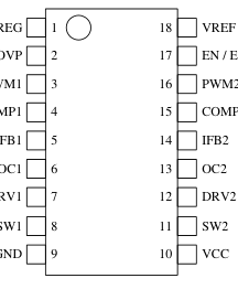
PWM1
COMP1
DRV1
Page 8
5. Typical Application Circuit
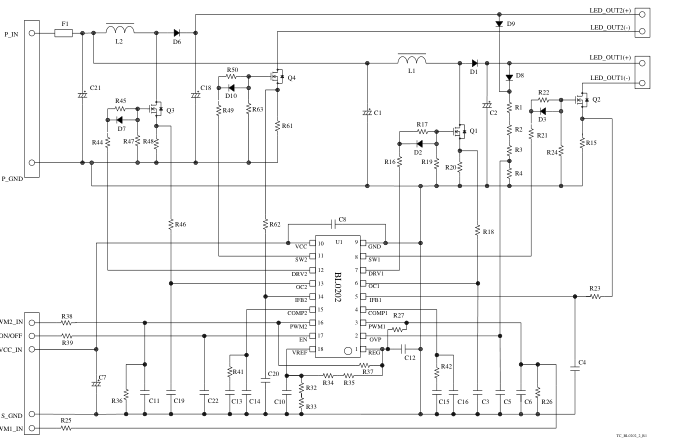
Figure 5-1 BL0202B and BL0202C Typical Application Circuit
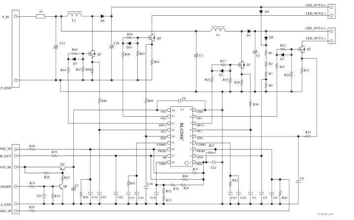
Figure 5-2 BL0200C Typical Application Circuit
Page 9
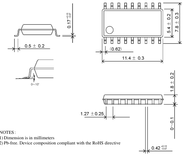
6. Package Diagram
SOP18
7. Marking Diagram
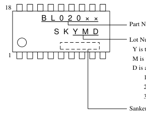
Part Number
Lot Number Y is the last digit of the year (0 to 9) M is the month (1 to 9, O, N or D) D is a period of days (1 to 3) : 1 : 1st to 10th 2 : 11th to 20th 3 : 21st to 31st
Sanken Control Number
Page 10
8. Functional Description
All of the parameter values used in these descriptions are typical values, unless they are specified as minimum or maximum. With regard to current direction, "+" indicates sink current (toward the IC) and "–" indicates source current (from the IC). The IC incorporates two boost converter circuits in one package, and can independently control each output current. The operation of control circuit for LED_OUT1 is same operation as the control circuit for LED_OUT2. When the one of output is not used, the control signal input pin (PWM, IFB and OC pin) of unused output should be connected to GND pin.
8.1 Startup Operation(BL0200C)
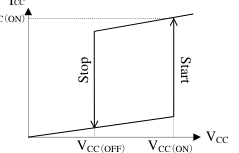
Figure 8-1 shows the VCC pin peripheral circuit. The VCC pin is the power supply input for control circuit from the external power supply. When the VCC pin voltage increases to the Operation Start Voltage, VCC(ON) = 9.6 V, the control circuit starts operation. After that, when the PWM pin voltage exceeds the PWM Pin ON Threshold Voltage, VPWM(ON) of 1.5 V (less than absolute maximum voltage of 5 V), the COMP Pin Charge Current at Startup, ICOMP(S) = −11 µA, flows from the COMP pin. This charge current flows to capacitors at the COMP pin. When the COMP pin voltage increases to the COMP Pin Voltage at Oscillation Start, VCOMP(ON) = 0.50 V or more, the control circuit
starts switching operation. As shown in Figure 8-2, when the VCC pin voltage decreases to the Operation Stop Voltage, VCC(OFF) = 9.1 V, the control circuit stops operation, by the UVLO (Undervoltage Lockout) circuit, and reverts to the state before startup.
External power supply
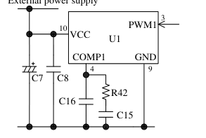
Figure 8-1 VCC pin peripheral circuit
ICC
ICC(ON)
Figure 8-2 VCC versus ICC
When the on-duty of the PWM dimming signal is small, the charge current at the COMP pin is controlled as follows in order to raise the output current quickly at startup. Figure 8-3 shows the operation waveform with the PWM dimming signal at startup.
VCC pin voltage
VCC(ON) 0
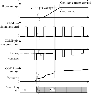
Figure 8-3 Startup operation during PWM dimming
While the IFB pin voltage increases to the IFB Pin Voltage at COMP Charge Switching, VIFB(COMP.VR), a capacitors at the COMP pin are charged by ICOMP(S) = −11 µA. During this period, they are charged by the COMP Pin Source Current, ICOMP(SRC) = −57 µA, when the PWM pin voltage is 1.5 V or more. Thus, the COMP pin voltage increases immediately. When the IFB pin voltage increases to VIFB(CMP1.VR) or more, the COMP pin source current is controlled according to the feedback amount, and the output current is controlled to be constant. The on-duty gradually becomes wide according to the
Page 11
increase of the COMP pin voltage, and the output power increases (Soft start operation). Thus, power stresses on components are reduced. When the VCC pin voltage decreases to the operation stop voltage or less, or the Auto Restart operation (see the Section 8.7 Protection Function) after protection is achieved, then the control circuit stops switching operation, and capacitors at the COMP pin are discharged by the COMP Pin Reset Current, ICOMP(R) = 360 µA simultaneously. The soft start operation is achieved at restart. The IC is operated by Auto Restart 1 at startup operation. See the Section 8.7 Protection Function about the caution of startup operation. VIFB(COMP.VR) is determined by the VREF pin voltage,
as shown in Figure 8-4. When VREF pin voltage is 1V, the value of VIFB(COMP.VR) becomes 0.60 V.
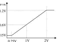
VIFB(COMP.VR)
VREF pin voltage
Figure 8-4 VREF pin voltage versus IFB pin voltage at
COMP charge switching
8.2 Startup Operation(BL0202B, BL0202C)
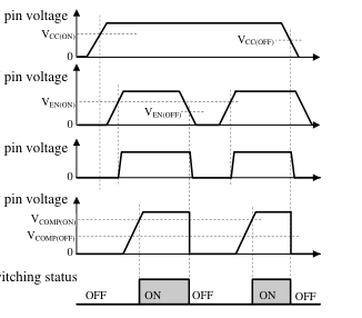
BL0202B and BL0202C have Enable Function. Figure 8-5 shows the peripheral circuit of VCC pin and EN pin, Figure 8-6 shows the operational waveforms. The VCC pin is the power supply input for control circuit from the external power supply. The EN pin is ON/OFF signal input from the external circuit. When the both VCC pin voltage, VCC, and EN pin voltage, VEN, increase to the each operation voltage or more, the control circuit starts operation (VCC ≥ VCC(ON) = 9.6 V and VEN ≥ VEN(ON) = 2.0 V). After that, when the PWM pin voltage exceeds the PWM Pin ON Threshold Voltage, VPWM(ON) of 1.5 V (less than absolute maximum voltage of 5 V), the COMP Pin Charge Current at Startup, ICOMP(S) = −11 µA, flows
from the COMP pin. This charge current flows to capacitors at the COMP pin. When the COMP pin voltage increases to the COMP Pin Voltage at Oscillation Start, VCOMP(ON) = 0.50 V or more, the control circuit starts switching operation. As shown in Figure 8-2, when the EN pin voltage decreases to the Operation Stop Voltage VEN(OFF) = 1.4 V or less, the control circuit stops operation. And when the
VCC pin voltage decreases to the Operation Stop Voltage, VCC(OFF) = 8.6 V, the control circuit stops operation, by the UVLO (Undervoltage Lockout) circuit, and reverts to the state before startup. The value of R39 connected to EN pin is set as follows;
V V (max) EN_ IN EN(ON)
R39 I (max) EN
V 6.2(V) EN_ IN
(8-1)
120(A)
Where, VEN_IN is EN pin input voltage (less than absolute value of EN pin voltage, 5 V ). VEN(ON)(max) is the maximum rating of EN Pin Operation Start Voltage. IEN(max) is the maximum rating of EN Pin Sink Current.
In case VEN_IN = 3.5V, the value of R39 should be set 7.5 kΩ or less.
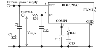
Figure 8-5 The peripheral circuit of VCC pin and EN pin
COMP pin voltage
Figure 8-6 Operational waveforms
Page 12
When the on-duty of the PWM dimming signal is small, the charge current at the COMP pin is controlled as follows in order to raise the output current quickly at startup. Figure 8-7 shows the operation waveform with the PWM dimming signal at startup.
VCC pin voltage
VCC(ON) 0
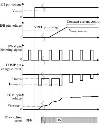
Figure 8-7 Startup operation during PWM dimming
While the IFB pin voltage increases to the IFB Pin Voltage at COMP Charge Switching, VIFB(COMP.VR), a capacitors at the COMP pin are charged by ICOMP(S) = −11 µA. During this period, they are charged by the COMP Pin Source Current, ICOMP(SRC) = −57 µA, when the PWM pin voltage is 1.5 V or more. Thus, the COMP pin voltage increases immediately. When the IFB pin voltage increases to VIFB(COMP.VR) or more, the COMP pin source current is controlled according to the feedback amount, and the output current is controlled constant. The on-duty gradually becomes wide according to the increase of the COMP pin voltage, and the output power increases (Soft start operation). Thus, power stresses on
components are reduced. When the VCC pin voltage or EN pin voltage decreases to the operation stop voltage or less, or the Auto Restart operation (see the Section 8.7 Protection Function) after protection is achieved, then the control circuit stops switching operation, and simultaneously
capacitors at the COMP pin are discharged by the COMP Pin Reset Current, ICOMP(R) = 360 µA. Because the on-duty gradually becomes wide after cycling power to the IC, the soft start operation is achieved at restart. The IC is operated by Auto Restart 1 at startup operation. See the Section 8.7 Protection Function about the caution of startup operation. VIFB(COMP.VR) is determined by the VREF pin voltage as shown in Figure 8-4.
8.3 Constant Current Control Operation
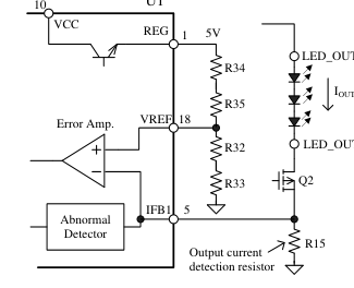
Figure 8-8 shows the IFB pin peripheral circuit. When the dimming MOSFET (Q2, Q4) turns on, the LED output current, IOUT(CC), is detected by the current detection resistor, R15 and R61. The IC compares the IFB pin voltage with the VREF pin voltage by the internal error amplifier, and controls the IFB pin voltage so that it gets close to the VREF pin voltage. The reference voltage at the VREF pin is the divided voltage of the REG pin voltage, VREG = 5 V, by R32 to R35, and thus this voltage can be externally adjusted. The setting current, IOUT(CC), of the LED_OUT can be calculated as follows.
V
(8-2)
I REF OUT (CC) R SEN
Where: VREF is the VREF pin voltage. The value is recommended to be 0.5 V to 2.0 V. RESN is the value of output current detection resistor
U1
IOUT(CC)
Figure 8-8 IFB pin peripheral circuit
Page 13
8.4 PWM Dimming Function
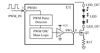
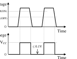
Figure 8-9 shows the peripheral circuit of PWM pin and SW pin. The PWM pin is used for the PWM dimming signal input. The SW pin drives the gate of external dimming MOSFET (Q2, Q4). The SW pin voltage is turned on / off by PWM signal and thus the dimming of LED is controlled by PWM signal input. As shown in Figure 8-10, when the PWM pin voltage becomes the PWM Pin ON Threshold Voltage, VPWM(ON) = 1.5 V or more, the SW pin voltage becomes VCC. When the PWM pin voltage becomes the PWM Pin OFF Threshold Voltage, VPWM(OFF) = 1.0 V or less, the SW pin voltage becomes 0.1 V or less. The PWM pin has the absolute maximum voltage of −0.3 V to 5 V, and the input impedance, RPWM, of 200 kΩ.
The PWM dimming signal should meet these specifications and threshold voltages of VPWM(ON) and VPWM(OFF).
LED_OUT1(−)
Figure 8-9 The peripheral circuit of PWM pin
and SW pin.
PWM pin voltage VPWM(ON) VPWM(OFF)
SW pin voltaege
Figure 8-10 The waveform of PWM pin and SW pin
8.5 Gate Drive
Figure 8-11 shows the peripheral circuit of DRV pin and SW pin and FSET pin. The DRV pin is for boost MOSFET, Q1 and Q3. The SW pin is for dimming MOSFET, Q2 and Q4. Table 8-1 shows drive voltages and currents of DRV pin and SW pin.
- Power MOSFET should be selected so that these VGS(th) threshold voltages are less than VCC enough over entire operating temperature range.
- Peripheral components of Power MOSFET, gate resistors and diode, affect losses of power MOSFET, gate waveform (ringing caused by the printed circuit board trace layout), EMI noise, and so forth, these values should be adjusted based on actual operation in the application.
- The resistors between gate and source (R19, R24, R47 and R63) are used to prevent malfunctions due to steep dv/dt at turn-off of the power MOSFET, and these resistors are connected near each the gate of the power MOSFETs and the ground line side of the current detection resistance. The reference value of them is from 10 kΩ to 100 kΩ.
Table 8-1 Drive voltage and current
| Pins | Drive voltage, V DRV | Drive current, I DRV | ||
| High | Low | Source | Sink | |
| DRV | V CC | ≤ 0.1 V | −0.36 A | 0.85 A |
| SW | V CC | ≤ 0.1 V | −85 mA | 220 mA |
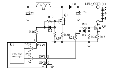
Figure 8-11 The peripheral circuit of DRV pin, SW pin and FSET pin
Page 14
8.6 Error Signal Output Function (BL0200C)
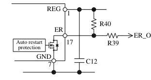
When an external circuit such as microcomputer uses the error signal output, configure the peripheral circuit of ER pin using the pull-up resistor, R40 and the protection resistor of ER pin, R39, as shown in Figure 8-12. The ER pin is connected to internal switch. When the protection function is active, the internal switch becomes OFF and ER_OUT becomes REG pin voltage from 0 V. The resistances of R39 and R40 are about 10 kΩ.
ER_OUT
Figure 8-12 ER pin peripheral circuit
8.7 Protection Function
As shown in Table 8-2, the IC performs protection operations according to kind of abnormal state. In all protection functions, when the fault condition is removed, the IC returns to normal operation automatically. The intermitted oscillation operation reduces stress on the power MOSFET, the secondary rectifier diode, and so forth.
Table 8-2 Relationship between a kind of abnormal state
and protection operations
| Abnormal States | Protection Operations | |
| 1 | Overcurrent of boost circuit (OCP) | Auto Restart 1 |
| 2 | Overcurrent of LED output (LED_OCP) | |
| 3 | Overvoltage of LED_OUT(+) (OVP) | |
| 4 | Short mode between LED_OUT(−) and GND | |
| 5 | Short mode of LED current detection resistor (R _Short) SEN | |
| 6 | Short mode of both ends of LED output | Auto Restart 2 |
| 7 | Open mode of LED current detection resistor (R _Open) SEN | |
| 8 | Overtemperature of junction of IC (TSD) | Auto Restart 3 |
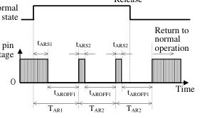
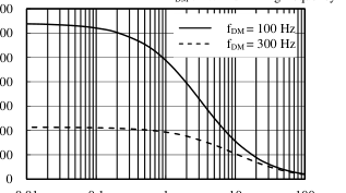
Auto Restart 1: As shown in Figure 8-13, the IC repeats an intermitted oscillation operation, after the detection of any one of abnormal states 1 to 5 in Table 8-2. This intermitted oscillation is determined by tARS1 or tARS2, and tAROFF1. The tARS1 is an oscillation time in the first intermitted oscillation cycle, TAR1. The tARS2 is an oscillation time in the second and subsequent intermitted oscillation cycle, TAR2. The tAROFF1 is a non-oscillation time in all intermitted oscillation cycle. In case PWM dimming frequency is low and the on-duty is small, the startup operation, the restart operation from on-duty = 0 % and the restart operation from intermitted oscillation operation need a long time.
Thus the value of tARS1 and tARS2 depend on frequency and on-duty of the PWM dimming signal, as shown in Figure 8-15 and Figure 8-16 for BL020×C, Figure 8-17 and Figure 8-18 for BL0202B.
Table 8-3 shows the Auto Restart 1 oscillation time, tARS1, tARS2, and the Auto Restart 1 non-oscillation time, tAROFF1, at on-duty = 100 %.
Table 8-3 Oscillation time and non-oscillation time
(at on-duty = 100 %)
| Oscillation time, t ARS1 | Oscillation time, t ARS2 | non-oscillation time, t AROFF1 | |
| BL0200C BL0202C | 31 ms | 20.5 ms | About 635 ms |
| BL0202B | 61.4 ms | 41.0 ms | About 1.3 s |
Auto Restart 2: As shown in Figure 8-14, the IC stops the switching operation immediately after the detection of abnormal states 6 or 7 in Table 8-2, and repeats an intermitted oscillation operation. In the intermitted oscillation cycle, the tARSW is an oscillation time, the tAROFF1 is a non-oscillation time. The value of tARSW is a few microseconds. The value of tARS2 is derived from Figure 8-18, and tAROFF2 is calculated as follows:
t t t
t
(8-3)
AROFF 2 ARS2 ARSW AROFF1
In case the on-duty is 100%, the value of tAROFF2 becomes as follows:
L0200C、BL0202C: tAROFF2 ≒ 20.5 + 635 = 655.5 (ms)
BL0202B: tAROFF2 ≒ 0.041 + 1.3 = 1.341 (s)
Page 15
Auto Restart 3:
The IC stops the switching operation immediately after
the detection of abnormal states 8 in Table 8-2, and keeps
a non-oscillation.
Release
Abnormal
SW pin voltage
Figure 8-13 Auto Restart 1
Release
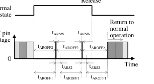
Abnormal
SW pin voltage
Figure 8-14 Auto Restart 2
fDM : PWM dimming frequency
2500
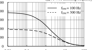
2000
1500
1000
0.01 0.1 1 10 100
Duty (%)
Figure 8-15 PWM dimming on-duty vs. tARS1 (BL020×C)
fDM : PWM dimming frequency
1400
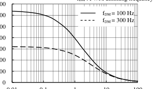
1200 1000
0.01 0.1 1 10 100
Duty (%)
Figure 8-16 PWM dimming on-duty vs. tARS2 (BL020×C)
fDM : PWM dimming frequency
2500
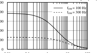
2000
1500
1000
0.01 0.1 1 10 100
Duty (%)
Figure 8-17 PWM dimming on-duty vs. tARS1 (BL0202B)
fDM : PWM dimming frequency
1400
1200 1000
0.01 0.1 1 10 100
Duty (%)
Figure 8-18 PWM dimming on-duty vs. tARS2 (BL0202B)
Page 16
The operating condition of Auto Restart 1 and 2 is as follows:
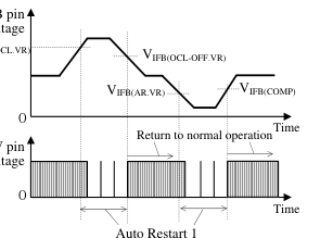
< The operating condition of Auto Restart 1 > The Auto Restart 1 is operated by the detection signals of the OC pin or IFB pin.
- Operation by the detection signal of OC pin: When the OC pin voltage increase to the OC Pin Overcurrent Protection Threshold Voltage, VOCP = 0.60 V, or more, the operation of the IC switches to Auto Restart 1. When the fault condition is removed and the OC pin voltage decreases to under VOCP, the IC returns to normal operation automatically.
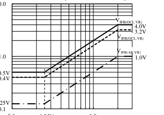
- Operation by the detection signal of IFB pin: As shown in Figure 8-19, IFB pin has two types of threshold voltage. These threshold voltages depend on the VREF pin voltage, as shown in Figure 8-20.
IFB pin voltage VIFB(OCL.VR)
SW pin voltage
Figure 8-19 IIFB pin threshold voltage and Auto Restart 1 operation
VIFB(OCL.VR) : IFB Pin Overcurrent Protection Low Threshold Voltage VIFB(OCL-OFF.VR) :IFB Pin Overcurrent Protection Release Threshold Voltage VIFB(AR.VR) :IFB Pin Auto Restart Operation Threshold Voltage 10.0
0.125V
0.1
1.0
0.25V VREF pin voltage (V)
Figure 8-20 VREF pin voltage versus IFB pin threshold voltages
1) In case IFB pin voltage increased When the FB pin voltage increase to VIFB(OCL.VR) in Figure 8-20, or more, the operation of the IC switches to Auto Restart 1. When the fault condition is removed and the IFB pin voltage decreases to VIFB(OCL-OFF.VR) in Figure 8-20, or less, the IC returns to normal operation automatically. 2) In case IFB pin voltage decreased When the FB pin voltage decrease to VIFB(AR.VR) in Figure 8-20, or more, the operation of the IC switches to Auto Restart 1. When the fault condition is removed and the IFB pin voltage increases to above VIFB(COMP), the IC returns to normal operation automatically.
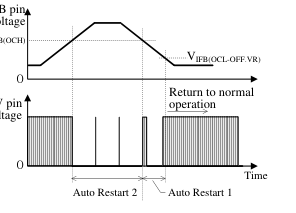
< The operating condition of Auto Restart 2 > The Auto Restart 2 is operated by the detection signal of the IFB pin. As shown in Figure 8-21, when the FB pin voltage increase to the IFB Pin Overcurrent Protection High Threshold Voltage, VIFB(OCH) = 4.0 V, or more, the operation of the IC switches to Auto Restart 2, and the IC stops switching operation immediately. When the fault condition is removed and the IFB pin voltage decreases to under VIFB(OCH), the operation of the IC switches to Auto Restart 1.
VIFB(OCH)
SW pin voltage
Figure 8-21 IFB pin threshold voltage and Auto Restart 2 operation
< Caution of startup operation > When the LED current is low and the IFB pin voltage is less than VIFB(AR.BR), during startup for example, the IC is operated by Auto Restart 1. If the startup time is too long, the IC operation becomes the intermitted oscillation by the Auto Restart 1. It becomes cause of the fault startup operation, thus the startup time should be set less than tARS1 in Figure 8-13.
Page 17
The protection operation according to the abnormal states in Table 8-2 is described in detail as follows:
8.7.1 Overcurrent of Boost Converter Part
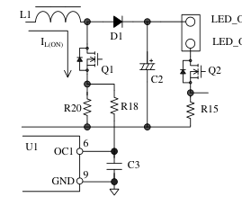
(OCP) When the OC pin detects the overcurrent of boost circuit, the IC switches to Auto Restart 1. Figure 8-22 shows the peripheral circuit of OC pin. When the boost MOSFET (Q1, Q3) turns on, the current flowing to L1 is detected by the current detection resistor (R20, R48), and the voltage on R4 is input to the OC pin. When the OC pin voltage increases to the OC Pin Overcurrent Protection Threshold Voltage, VOCP = 0.60 V or more, the on-duty becomes narrow by pulse-by-pulse basis, and the output power is limited.
LED_OUT1(+)
LED_OUT1(-)
Figure 8-22 OC pin peripheral circuit
8.7.2 Overcurrent of LED Output
(LED_OCP)
Figure 8-23 shows the peripheral circuit of IFB pin and COMP pin. When the dimming MOSFET (Q2, Q4) turns on, the output current is detected by the detection resistor (R15, R61). When the boost operation cannot be done by failure such as short circuits in LED string, the IFB pin voltage is increased by the increase of LED current. There are three types of operation modes in LED_OCP state.
(1) When the IFB pin voltage is increased by the increase of LED current, COMP pin voltage is decreases. In addition, when the COMP pin voltage decreases to the COMP Pin Voltage at Oscillation Stop, VCOMP(OFF) = 0.25 V or less, the IC stops switching operation, and limits the increase of the output current. When IFB pin voltage is decreased by the decrease of LED current, COMP pin voltage increases. When COMP pin voltage becomes VCOMP(ON) = 0.50 V or more, the IC restarts switching operation.
(2) When IFB pin voltage becomes VIFB(OCL.VR) or more (see Figure 8-20), the IC switches to Auto Restart 1.
(3) The LED current increases further and when the IFB pin voltage increases to the IFB Pin Overcurrent Protection High Threshold Voltage, VIFB(OCH) = 4.0 V or more, the IC switches to Auto Restart 2.
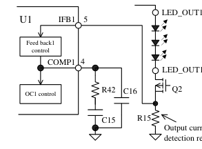
Figure 8-23 The peripheral circuit of IFB pin
and COMP pin
8.7.3 Overvoltage of LED_OUT (+) (OVP)
The OVP pin detects LED_OUT (+) voltage as shown in Figure 8-24. When the LED_OUT (+) or the IFB pin is open and the OVP pin voltage increases to the OVP Pin Overvoltage Protection Threshold Voltage, VOVP = 3.00 V, the IC immediately stops switching operation. When the OVP pin voltage decreases to the OVP Pin Overvoltage Protection Release Threshold Voltage, VOVP(OFF) = 2.75 V or the IFB pin voltage decreases to VIFB(AR.VR) in Figure 8-20, then the IC switches to Auto Restart 1.
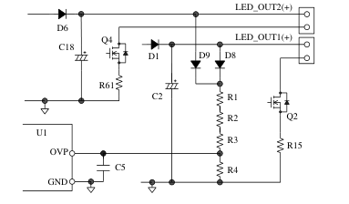
Figure 8-24 OVP pin peripheral circuit
Page 18
8.7.4 Short Mode between LED_OUT(−)
and GND
When the LED_OUT (–) and the GND are shorted, and the IFB pin voltage decreases to VIFB(AR.VR) in Figure 8-20, then the IC switches to Auto Restart 1.
8.7.5 Short Mode of LED Current Detection
Resistor (RSEN_Short)
When the output current detection resistor (R15, R61), is shorted, the IFB pin voltage decreases. When the IFB pin voltage decreases to VIFB(AR.VR) in Figure 8-20, then the IC switches to Auto Restart 1.
8.7.6 Short Mode of LED Output Both Ends
When the LED_OUT (+) and LED_OUT (–) are shorted, the short current flows through the output current detection resistor (R15, R61), while the dimming MOSFET (Q2, Q4) turns on. The IFB pin detects the voltage rise of the detection resistor. When the IFB pin voltage increases to the IFB Pin Overcurrent Protection High Threshold Voltage, VIFB(OCH) = 4.0 V or more, the IC switches to Auto Restart 2.
8.7.7 Open Mode of LED Current Detection
Resistor (RSEN_Open)
When the output current detection resistor (R15, R61), is open, the IFB pin voltage increases. When the IFB pin voltage increases to the IFB Pin Overcurrent Protection High Threshold Voltage, VIFB(OCH) = 4.0 V or more, the IC switches to Auto Restart 2.
8.7.8 Overtemperature of junction of IC
(TSD) When the temperature of the IC increases to Tj(TSD) = 125 °C (min) or more, the TSD is activated, and the IC stops switching operation. When the junction temperature decreases by Tj(TSD) − Tj(TSD)HYS after the fault condition is removed, the IC returns to normal operation automatically.
9. Design Notes
9.1 Peripheral Components
Take care to use the proper rating and proper type of components. Input and output electrolytic capacitors, C1, C2, C18 and C21 ▫ Apply proper design margin to accommodate ripple current, voltage, and temperature rise. ▫ Use of high ripple current and low impedance types, designed for switch-mode power supplies, is recommended, depending on their purposes. Inductor, L1, L2 ▫ Apply proper design margin to temperature rise by core loss and copper loss. ▫ Apply proper design margin to core saturation. Current detection resistors, R15, R20, R48 and R61 Choose a type of low internal inductance because a high frequency switching current flows to the current detection resistor, and of properly allowable
dissipation.
9.2 Inductor Design Parameters
The CRM\* or DCM\* mode of boost converter with PWM dimming can improve the output current rise during PWM dimming. \* CRM is the critical conduction mode, DCM is the discontinuous conduction mode.
(1) On-duty Setting The output voltage of boost converter is more than the input voltage. The on-duty, DON can be calculated using following equation. The equality of the equation means the condition of CRM mode operation and the inequality means that of DCM mode operation.
V V DON OUT IN
(9-1)
V OUT
where: VIN is the minimum input voltage, VOUT is the maximum forward voltage drop of LED string.
DON is selected by the above equation applied to CRM or DCM mode. In case fPWM = 100 kHz, the range of DON should be 3.1 % to 90 %. In case fPWM = 200 kHz, the range of DON should be 6 % to 90 %. (The minimum value results from the condition of tMIN, and fPWM. The maximum value is DMAX).
Page 19
(2) Inductance value, L The inductance value, L, for DCM or CRM mode can be calculated as follow:
V D 2
L
(9-2)
IN ON
2 I f V V OUT PWM OUT IN
where: IOUT is the maximum output current, fPWM is the maximum operation frequency of PWM
(3) Peak inductor current, ILP
V D I IN ON
(9-3)
LP L f PWM
(4) Inductor selection The inductor should be applied the value of inductance, L, from equation (9-2) and the DC superimposition characteristics being higher than the peak inductor current, ILP, from equation (9-3).
9.3 PCD Trace Layout and Component
Placement
Since the PCB circuit trace design and the component layout significantly affects operation, EMI noise, and power dissipation, the high frequency PCB trace as shown in Figure 9-1 should be low impedance with small loop and wide trace.
D1
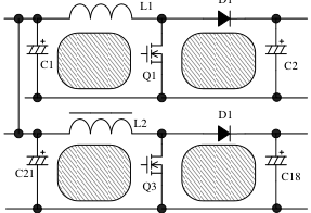
Figure 9-1 High-frequency current loops
(hatched areas)
In addition, the ground traces affect radiated EMI noise, and wide, short traces should be taken into account. Figure 9-2 shows the circuit design example of BL0200C.
(1) Main Circuit Trace Layout This is the main trace containing switching currents, and thus it should be as wide trace and small loop as possible. C1 and C18 should be connected near the inductors, L1and L2, in order to reduce impedance of the high frequency current loop.
(2) Control Ground Trace Layout Since the operation of IC may be affected from the large current of the main trace that flows in control ground trace, the control ground trace should be connected at a single point grounding of point A with a dedicated trace.
(3) Current Detection Resistor Trace Layout R15, R20, R48 and R61 are current detection resistors. The trace from the base of current detection resistor should be connected to the pin of IC with a dedicated trace.
(4) COMP pin Trace Layout for Compensation Component The components connected to COMP pin are compensation components. The trace of the compensation component should be connected as close as possible to COMP pin, to reduce the influence of noise.
(5) Bypass Capacitor Trace Layout on VCC , REG, and VREF pins C8, C12 and C10 of bypass capacitors, connected to VCC, REG, and VREF pins respectively, should be connected as close as possible to the pin of IC, to reduce the influence of noise.
(6) Power MOSFET Gate Trace Layout The resistor between gate and source, R19, R24, R47 and R63, should be connected near each the gate of the power MOSFETs and the ground line side of the current detection resistance. Peripheral components of MOSFET, gate resistors and diodes, should be connected as close as possible between each the gate of the power MOSFETs and the pin of IC.
Page 20
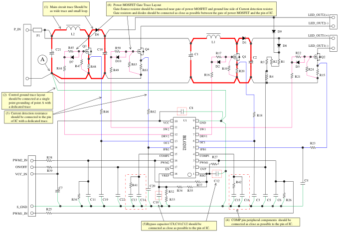
Figure 9-2 Peripheral circuit example around the IC (BL0200C)
Page 21
10.Reference Design of Power Supply
As an example, the following show a power supply specification of BL0200C and BL0202B, circuit schematic, bill of materials, and transformer specification. This reference design is the example of the value of parts, and should be adjusted based on actual operation in the application.
10.1 BL0202B BL0202B Features - DRV pin oscillation frequency is 100 kHz - Enable function Power Supply Specification
| IC | BL0202B |
| Input voltage | DC 24 V |
| Maximum output power | 40 W (max.) |
| Output voltage | 50 V |
| Output current | 400 mA × 2 |
Circuit
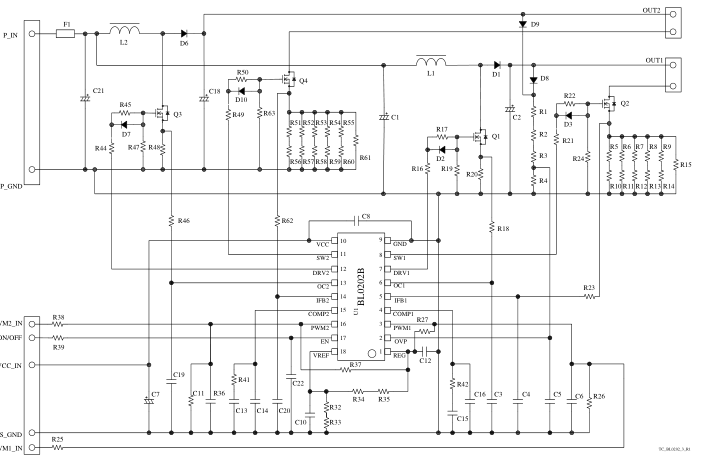
Page 22
Bill of Materials
| Symbol | Part type | Ratings(1) | Recommended Sanken Parts | Symbol | Part type | Ratings(1) | Recommended Sanken Parts |
|---|---|---|---|---|---|---|---|
| F1 | Fuse | 3 A | R4 | General, chip, 2012 | 11 kΩ | ||
| L1 | Inductor | 50 μH, 3 A | R5-R14 | General, chip, 2012 | Open | ||
| L2 | Inductor | 50 μH, 3 A | R15 | General | 1.35 Ω, 1 W | ||
| D1 | Fast recovery | 200 V, 1.5 A | EL 1Z | R16 | General, chip, 2012 | 10 Ω | |
| D2 | Schottky | 30 V, 1 A | SJPA-D3 | R17 | General, chip, 2012 | 100 Ω | |
| D3 | Schottky | 30 V, 1 A | SJPA-D3 | R18 (2) | General, chip, 2012 | 100 Ω | |
| D6 | Fast recovery | 200 V, 1.5 A | EL 1Z | R19 | General, chip, 2012 | 10 kΩ | |
| D7 | Schottky | 30 V, 1 A | SJPA-D3 | R20 | General | 0.22 Ω, 2 W | |
| D8 | 200 V, 1 A | AL01Z | R21 | General, chip, 2012 | 470 Ω | ||
| D10 | Schottky | 30 V, 1 A | SJPA-D3 | R22 | General, chip, 2012 | 1.5 kΩ | |
| Q1 | Power MOSFET | 200 V, 45 mΩ (typ.) | SKP202 | R23 | General, chip, 2012 | 1.5 kΩ | |
| Q2 | Power MOSFET | 100 V, 1 Ω (typ.) | R24 | General, chip, 2012 | 10 kΩ | ||
| Q3 | Power MOSFET | 200 V, 45 mΩ (typ.) | SKP202 | R25 | General, chip, 2012 | 1 kΩ | |
| Q4 | Power MOSFET | 100 V, 1 Ω (typ.) | R26 | General, chip, 2012 | 33 kΩ | ||
| C1 | Electrolytic | 50 V, 22 μF | R27 | General, chip, 2012 | 10 kΩ | ||
| C2 | Electrolytic | 100 V, 100 μF | R32 | General, chip, 2012 | 10 kΩ | ||
| C3 (2) | Ceramic, chip, 2012 | 100 pF | R33 | General, chip, 2012 | 0 Ω | ||
| C4 (2) | Ceramic, chip, 2012 | 100 pF | R34 | General, chip, 2012 | 82 kΩ | ||
| C5 | Ceramic, chip, 2012 | 10 nF | R35 (2) | General, chip, 2012 | 560 Ω | ||
| C6 | Ceramic, chip, 2012 | 470 pF | R37 | General, chip, 2012 | 10 kΩ | ||
| C7 | Electrolytic | 50 V, 100 μF | R38 | General, chip, 2012 | 1 kΩ | ||
| C8 | Ceramic, chip, 2012 | 50 V, 0.1 μF | R39 | General, chip, 2012 | 5 kΩ (V = 3.5 V) EN | ||
| C9 | Ceramic, chip, 2012 | 50 V, 0.1 μF | R40 | General, chip, 2012 | 10 kΩ | ||
| C10 | Ceramic, chip, 2012 | 0.1 μF | R41 (2) | General, chip, 2012 | 22 kΩ | ||
| C11 | Ceramic, chip, 2012 | 470 pF | R42 (2) | General, chip, 2012 | 22 kΩ | ||
| C12 | Ceramic, chip, 2012 | 0.1 μF | R44 | General, chip, 2012 | 10 Ω | ||
| C13 (2) | Ceramic, chip, 2012 | 0.047 μF | R45 | General, chip, 2012 | 100 Ω | ||
| C14 (2) | Ceramic, chip, 2012 | 2200 pF | R46 (2) | General, chip, 2012 | 100 Ω | ||
| C15 (2) | Ceramic, chip, 2012 | 0.047 μF | R47 | General, chip, 2012 | 10 kΩ | ||
| C16 (2) | Ceramic, chip, 2012 | 2200 pF | R48 | General | 0.22 Ω, 2 W | ||
| C18 | Electrolytic | 100 V, 100 μF | R49 | General, chip, 2012 | 470 Ω | ||
| C19 (2) | Ceramic, chip, 2012 | 100 pF | R50 | General, chip, 2012 | 1.5 kΩ | ||
| C20 (2) | Ceramic, chip, 2012 | 100 pF | R51-R60 | General, chip, 2012 | Open | ||
| C21 | Electrolytic | 50 V, 22 μF | R61 | General | 1.35 Ω, 1 W | ||
| C22 | Ceramic, chip, 2012 | 0.1 μF | R62 | General, chip, 2012 | 1.5 kΩ | ||
| R1 (3) | General, chip, 2012 | 110 kΩ | R63 | General, chip, 2012 | 10 kΩ | ||
| R2 (3) | General, chip, 2012 | 110 kΩ | U1 | IC | BL0202B | ||
| R3 (3) | General, chip, 2012 | 0 Ω |
(1) Unless otherwise specified, the voltage rating of capacitor is 50V or less, and the power rating of resistor is 1/8W or less. (2) It is necessary to be adjusted based on actual operation in the application. (3) Resistors applied high DC voltage and of high resistance are recommended to select resistors designed against electromigration or use combinations of resistors in series for that to reduce each applied voltage, according to the requirement of the application.
Page 23
10.2 BL0200C BL0200C Features - DRV pin oscillation frequency is 200 kHz - Error signal output Power Supply Specification
| IC | BL0200C |
| Input voltage | DC 24 V |
| Maximum output power | 40 W (max.) |
| Output voltage | 50 V |
| Output current | 400 mA × 2 |
Circuit Schematic
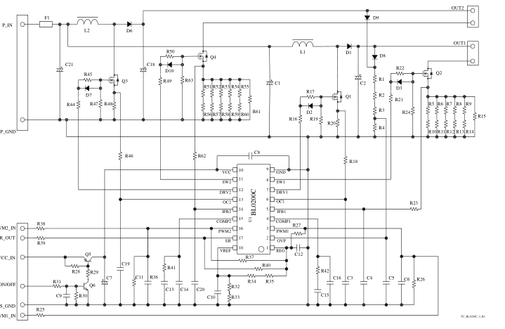
Page 24
Bill of Materials
| Symbol | Part type | Ratings(1) | Recommended Sanken Parts | Symbol | Part type | Ratings(1) | Recommended Sanken Parts |
|---|---|---|---|---|---|---|---|
| F1 | Fuse | 3 A | R5-R14 | General, chip, 2012 | Open | ||
| L1 | Inductor | 25 μH, 3 A | R15 | General | 1.35 Ω, 1 W | ||
| L2 | Inductor | 25 μH, 3 A | R16 | General, chip, 2012 | 10 Ω | ||
| D1 | Fast recovery | 200 V, 1.5 A | EL 1Z | R17 | General, chip, 2012 | 100 Ω | |
| D2 | Schottky | 30 V, 1 A | SJPA-D3 | R18 (2) | General, chip, 2012 | 100 Ω | |
| D3 | Schottky | 30 V, 1 A | SJPA-D3 | R19 | General, chip, 2012 | 10 kΩ | |
| D6 | Fast recovery | 200 V, 1.5 A | EL 1Z | R20 | General | 0.22 Ω, 2 W | |
| D7 | Schottky | 30 V, 1 A | SJPA-D3 | R21 | General, chip, 2012 | 470 Ω | |
| D8 | 200 V, 1 A | AL01Z | R22 | General, chip, 2012 | 1.5 kΩ | ||
| D9 | 200 V, 1 A | AL01Z | R23 | General, chip, 2012 | 1.5 kΩ | ||
| D10 | Schottky | 30 V, 1 A | SJPA-D3 | R24 | General, chip, 2012 | 10 kΩ | |
| Q1 | Power MOSFET | 200 V, 45 mΩ (typ.) | SKP202 | R25 | General, chip, 2012 | 1 kΩ | |
| Q2 | Power MOSFET | 100 V, 1 Ω (typ.) | R26 | General, chip, 2012 | 33 kΩ | ||
| Q3 | Power MOSFET | 200 V, 45 mΩ (typ.) | SKP202 | R27 | General, chip, 2012 | 10 kΩ | |
| Q4 | Power MOSFET | 100 V, 1 Ω (typ.) | R28 | General, chip, 2012 | 10 kΩ | ||
| Q5 | PNP Transistor | −50 V, 0.1 A | R29 | General, chip, 2012 | 12 kΩ | ||
| Q6 | NPN Transistor | 50 V, 0.1 A | R30 | General, chip, 2012 | 10 kΩ | ||
| C1 | Electrolytic | 50 V, 22 μF | R31 | General, chip, 2012 | 15 kΩ | ||
| C2 | Electrolytic | 100 V, 47 μF | R32 | General, chip, 2012 | 10 kΩ | ||
| C3 (2) | Ceramic, chip, 2012 | 100 pF | R33 | General, chip, 2012 | 0 Ω | ||
| C4 (2) | Ceramic, chip, 2012 | 100 pF | R34 | General, chip, 2012 | 82 kΩ | ||
| C5 | Ceramic, chip, 2012 | 10 nF | R35 | General, chip, 2012 | 560 Ω | ||
| C6 | Ceramic, chip, 2012 | 470 pF | R36 | General, chip, 2012 | 33 kΩ | ||
| C7 | Electrolytic | 50 V, 100 μF | R37 | General, chip, 2012 | 10 kΩ | ||
| C8 | Ceramic, chip, 2012 | 50 V, 0.1 μF | R38 | General, chip, 2012 | 1 kΩ | ||
| C9 | Ceramic, chip, 2012 | 50 V, 0.1 μF | R39 | General, chip, 2012 | 10 kΩ | ||
| C10 | Ceramic, chip, 2012 | 0.1 μF | R40 | General, chip, 2012 | 10 kΩ | ||
| C11 | Ceramic, chip, 2012 | 470 pF | R41 (2) | General, chip, 2012 | 22 kΩ | ||
| C12 | Ceramic, chip, 2012 | 0.1 μF | R42 (2) | General, chip, 2012 | 22 kΩ | ||
| C13 (2) | Ceramic, chip, 2012 | 0.047 μF | R44 | General, chip, 2012 | 10 Ω | ||
| C14 (2) | Ceramic, chip, 2012 | 2200 pF | R45 | General, chip, 2012 | 100 Ω | ||
| C15 (2) | Ceramic, chip, 2012 | 0.047 μF | R46 (2) | General, chip, 2012 | 100 Ω | ||
| C16 (2) | Ceramic, chip, 2012 | 2200 pF | R47 | General, chip, 2012 | 10 kΩ | ||
| C18 | Electrolytic | 100 V, 47 μF | R48 | General | 0.22 Ω, 2 W | ||
| C19 (2) | Ceramic, chip, 2012 | 100 pF | R49 | General, chip, 2012 | 470 Ω | ||
| C20 (2) | Ceramic, chip, 2012 | 100 pF | R50 | General, chip, 2012 | 1.5 kΩ | ||
| C21 | Electrolytic | 50 V, 22 μF | R51-R60 | General, chip, 2012 | Open | ||
| R1 (3) | General, chip, 2012 | 110 kΩ | R61 | General | 1.35 Ω, 1 W | ||
| R2 (3) | General, chip, 2012 | 110 kΩ | R62 | General, chip, 2012 | 1.5 kΩ | ||
| R3 (3) | General, chip, 2012 | 0 Ω | R63 | General, chip, 2012 | 10 kΩ | ||
| R4 | General, chip, 2012 | 11 kΩ | U1 | IC | BL0200C |
(1) Unless otherwise specified, the voltage rating of capacitor is 50V or less, and the power rating of resistor is 1/8W or less. (2) It is necessary to be adjusted based on actual operation in the application. (3) Resistors applied high DC voltage and of high resistance are recommended to select resistors designed against electromigration or use combinations of resistors in series for that to reduce each applied voltage, according to the requirement of the application.
Page 25
OPERATING PRECAUTIONS
In the case that you use Sanken products or design your products by using Sanken products, the reliability largely depends on the degree of derating to be made to the rated values. Derating may be interpreted as a case that an operation range is set by derating the load from each rated value or surge voltage or noise is considered for derating in order to assure or improve the reliability. In general, derating factors include electric stresses such as electric voltage, electric current, electric power etc., environmental stresses such as ambient temperature, humidity etc. and thermal stress caused due to self-heating of semiconductor products. For these stresses, instantaneous values, maximum values and minimum
values must be taken into consideration. In addition, it should be noted that since power devices or IC’s including power devices have large self-heating value, the degree of derating of junction temperature affects the reliability significantly.
Because reliability can be affected adversely by improper storage environments and handling methods, please observe the following cautions. Cautions for Storage Ensure that storage conditions comply with the standard temperature (5 to 35°C) and the standard relative humidity (around 40 to 75%); avoid storage locations that experience extreme changes in temperature or humidity. Avoid locations where dust or harmful gases are present and avoid direct sunlight. Reinspect for rust on leads and solderability of the products that have been stored for a long time. Cautions for Testing and Handling When tests are carried out during inspection testing and other standard test periods, protect the products from power
surges from the testing device, shorts between the product pins, and wrong connections. Ensure all test parameters are within the ratings specified by Sanken for the products. Soldering When soldering the products, please be sure to minimize the working time, within the following limits:
- 260 ± 5 °C
10 ± 1 s (Flow, 2 times)
- 380 ± 10 °C 3.5 ± 0.5 s (Soldering iron, 1 time)
Electrostatic Discharge When handling the products, the operator must be grounded. Grounded wrist straps worn should have at least 1MΩ of resistance from the operator to ground to prevent shock hazard, and it should be placed near the operator. Workbenches where the products are handled should be grounded and be provided with conductive table and floor mats. When using measuring equipment such as a curve tracer, the equipment should be grounded. When soldering the products, the head of soldering irons or the solder bath must be grounded in order to prevent leak voltages generated by them from being applied to the products. The products should always be stored and transported in Sanken shipping containers or conductive containers, or
be wrapped in aluminum foil.
Page 26
IMPORTANT NOTES
The contents in this document are subject to changes, for improvement and other purposes, without notice. Make sure that this is the latest revision of the document before use. Application and operation examples described in this document are quoted for the sole purpose of reference for the use of the products herein and Sanken can assume no responsibility for any infringement of industrial property rights, intellectual property rights or any other rights of Sanken or any third party which may result from its use. Unless otherwise agreed in writing by Sanken, Sanken makes no warranties of any kind, whether express or implied, as to the products, including product merchantability, and fitness for a particular purpose and
special environment, and the information, including its accuracy, usefulness, and reliability, included in this document. Although Sanken undertakes to enhance the quality and reliability of its products, the occurrence of failure and defect of semiconductor products at a certain rate is inevitable. Users of Sanken products are requested to take, at their own risk, preventative measures including safety design of the equipment or systems against any possible injury, death, fires or damages to the society due to device failure or malfunction. Sanken products listed in this document are designed and intended for the use as components in general purpose electronic equipment or apparatus (home appliances, office equipment, telecommunication
equipment, measuring equipment, etc.). When considering the use of Sanken products in the applications where higher reliability is required (transportation equipment and its control systems, traffic signal control systems or equipment, fire/crime alarm systems, various safety devices, etc.), and whenever long life expectancy is required even in general purpose electronic equipment or apparatus, please contact your nearest Sanken sales representative to discuss, prior to the use of the products herein. The use of Sanken products without the written consent of Sanken in the applications where extremely high reliability is required (aerospace equipment, nuclear power control systems, life support systems, etc.) is
strictly prohibited. When using the products specified herein by either (i) combining other products or materials therewith or (ii) physically, chemically or otherwise processing or treating the products, please duly consider all possible risks that may result from all such uses in advance and proceed therewith at your own responsibility. Anti radioactive ray design is not considered for the products listed herein. Sanken assumes no responsibility for any troubles, such as dropping products caused during transportation out of Sanken’s distribution network. The contents in this document must not be transcribed or copied without Sanken’s written consent.