


 Download PDF
BD241C_11 ONSEMI
Document overview
- PDF pages: 6
Technical content
Page 1
BD241C (NPN), BD242B (PNP), BD242C (PNP)
Complementary Silicon
Plastic Power Transistors
Designed for use in general purpose amplifier and switching
applications.
Features
- Collector−Emitter Saturation Voltage −
VCE = 1.2 Vdc (Max) @ IC = 3.0 Adc
- Collector−Emitter Sustaining Voltage −
VCEO(sus) = 100 Vdc (Min) BD241C, BD242C
- High Current Gain − Bandwidth Product
fT = 3.0 MHz (Min) @ IC = 500 mAdc
- Compact TO−220 AB Package
- Epoxy Meets UL94 V−0 @ 0.125 in
- ESD Ratings: Human Body Model, 3B ? 8000 V
Machine Model, C ? 400 V
- Pb−Free Packages are Available\*
MAXIMUM RATINGS
| ÎÎÎÎÎÎÎÎÎÎÎÎÎÎ Rating ÎÎÎÎÎÎÎ | ÎÎÎÎÎÎÎÎ Symbol ÎÎÎÎÎ | ÎÎÎÎÎÎÎ BD242B ÎÎÎÎ | ÎÎBD2ÎÎ41CÎÎÎ BD242C ÎÎÎÎ | ÎÎÎÎ Unit ÎÎ |
|---|---|---|---|---|
| Collector−Emitter Voltage ÎÎÎÎÎÎÎÎÎÎÎÎÎÎ | VCEO ÎÎÎÎÎÎÎÎÎÎ | 80 ÎÎÎÎÎÎÎÎ | 100 ÎÎÎÎÎÎÎÎ | Vdc ÎÎÎÎ |
| Collector−Emitter Voltage ÎÎÎÎÎÎÎÎÎÎÎÎÎÎ | VCES ÎÎÎÎÎÎÎÎÎÎ | 90 ÎÎÎÎÎÎÎÎ | 115 ÎÎÎÎÎÎÎÎ | Vdc ÎÎÎÎ |
| Emitter−Base Voltage ÎÎÎÎÎÎÎÎÎÎÎÎÎÎ | VEB ÎÎÎÎÎÎÎÎÎÎ | 5.0 ÎÎÎÎÎÎÎÎÎÎÎÎÎÎÎ | Vdc ÎÎÎÎ | |
| Collector Current ÎÎÎÎÎÎCoÎÎntinÎÎuousÎÎÎÎ Peak ÎÎÎÎÎÎÎ | IC ÎÎÎÎÎÎÎÎÎÎ ÎÎÎÎÎ | ÎÎÎÎÎÎ3.0ÎÎÎÎÎÎÎÎ 5.0 ÎÎÎÎÎÎÎ | Adc ÎÎÎÎ ÎÎ | |
| Base Current ÎÎÎÎÎÎÎÎÎÎÎÎÎÎ | IB ÎÎÎÎÎÎÎÎÎÎ | 1.0 ÎÎÎÎÎÎÎÎÎÎÎÎÎÎ | Adc ÎÎÎÎ | |
| Total Device Dissipation @ ÎÎTC =ÎÎ 25ÎΰC ÎÎÎÎÎÎÎÎ Derate above 25°C ÎÎÎÎÎÎÎ | PD ÎÎÎÎÎÎÎÎÎÎ ÎÎÎÎÎ | 40 ÎÎÎÎÎÎÎÎÎÎÎÎÎÎ ÎÎÎ0.32ÎÎÎÎ | W ÎÎÎÎ ÎW/°ÎC | |
| ÎÎOpeÎÎratinÎÎg anÎÎd SÎÎtoragÎÎe ÎÎ Junction Temperature Range ÎÎÎÎÎÎÎ | ÎÎÎÎTJÎÎ, TstÎÎÎÎg ÎÎÎÎÎ | ÎÎÎΖ65ÎÎ to +ÎÎ150ÎÎÎÎÎÎ ÎÎÎÎÎÎÎ | ÎΰCÎÎ ÎÎ |
THERMAL CHARACTERISTICS

Stresses exceeding Maximum Ratings may damage the device. Maximum Ratings are stress ratings only. Functional operation above the Recommended Operating Conditions is not implied. Extended exposure to stresses above the Recommended Operating Conditions may affect device reliability.
\*For additional information on our Pb−Free strategy and soldering details, please download the ON Semiconductor Soldering and Mounting Techniques Reference Manual, SOLDERRM/D.
© Semiconductor Components Industries, LLC, 2011 October, 2011 − Rev. 8

POWER TRANSISTORS
COMPLEMENTARY
SILICON
3 AMP
80−100 VOLTS
40 WATTS
MARKING DIAGRAM
TO−220AB
CASE 221A−09
AYWW
STYLE 1
BD24xxG
1 2 3
BD24xx = Device Code xx = 1C, 2B, or 2C A = Assembly Location Y = Year WW = Work Week G = Pb−Free Package
ORDERING INFORMATION
| Column 1 | Column 2 | Column 3 |
|---|---|---|
| Device | Package | Shipping |
| BD241C | TO−220AB | 50 Units/Rail |
| BD241CG | TO−220AB (Pb−Free) | 50 Units/Rail |
| BD242B | TO−220AB | 50 Units/Rail |
| BD242BG | TO−220AB (Pb−Free) | 50 Units/Rail |
| BD242C | TO−220AB | 50 Units/Rail |
| BD242CG | TO−220AB (Pb−Free) | 50 Units/Rail |
Publication Order Number:
BD241C/D
Page 2
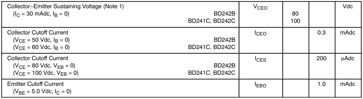
ELECTRICAL CHARACTERISTICS (TC = 25°C unless otherwise noted)
Characteristic
Symbol
Min Max Unit
OFF CHARACTERISTICS
ON CHARACTERISTICS (Note 1)
| Column 1 | Column 2 | Column 3 | Column 4 | Column 5 |
|---|---|---|---|---|
| DC Current Gain ÎÎ(ÎÎIC =ÎÎ 1.0 ÎÎAdc,ÎÎ VCEÎÎ = 4ÎÎ.0 VdÎÎc) ÎÎÎÎÎÎÎÎÎÎÎÎÎÎÎÎÎÎÎÎÎÎÎÎÎÎ (IC = 3.0 Adc, VCE = 4.0 Vdc) ÎÎÎÎÎÎÎÎÎÎÎÎÎÎÎÎÎÎÎÎÎ | hFE ÎÎÎÎÎÎÎÎÎÎ ÎÎÎÎÎÎ | ÎÎ2ÎÎ5 10 ÎÎ | ÎÎÎÎÎÎÎÎ ÎÎÎÎÎ | ÎÎÎÎ ÎÎ |
| Collector−Emitter Saturation Voltage ÎÎÎÎÎÎÎÎÎÎÎÎÎÎÎÎÎÎÎÎÎÎÎÎÎÎÎÎÎÎÎÎÎÎÎÎÎÎÎÎÎÎ (IC = 3.0 Adc, IB = 0.6 Adc) ÎÎÎÎÎÎÎÎÎÎÎÎÎÎÎÎÎÎÎÎÎ | ÎÎÎÎÎÎVCEÎÎ(sat)ÎÎÎÎ ÎÎÎÎÎÎ | ÎÎÎÎ ÎÎ | 1.2 ÎÎÎÎÎÎÎÎÎÎ ÎÎÎÎÎ | Vdc ÎÎÎÎ ÎÎ |
| Base−Emitter On Voltage ÎÎ(ÎÎIC =ÎÎ 3.0 ÎÎAdc,ÎÎ VCEÎÎ = 4ÎÎ.0 VdÎÎc) ÎÎÎÎÎÎÎÎÎÎÎÎÎÎÎÎÎÎÎÎÎÎÎÎÎÎ | VBE(on) ÎÎÎÎÎÎÎÎÎÎÎÎ | ÎÎÎÎ | 1.8 ÎÎÎÎÎÎÎÎÎÎ | Vdc ÎÎÎÎ |
DYNAMIC CHARACTERISTICS
| Column 1 | Column 2 | Column 3 | Column 4 | Column 5 |
|---|---|---|---|---|
| ÎÎCuÎÎrrentÎÎ GaiÎÎn − BÎÎandÎÎwidtÎÎh PrÎÎoducÎÎt (NÎÎote 2ÎÎ) ÎÎÎÎÎÎÎÎÎÎÎÎÎÎÎÎÎÎÎÎ Î( ÎIC = Î 500 Î mAd Îc, V ÎCE = Î 10 ÎVdc, Î ftestÎ = 1. Î0 MH Îz) ÎÎÎÎÎÎÎÎÎ | ÎÎÎÎÎfTÎÎÎÎÎ ÎÎÎÎÎÎ | ÎÎ3ÎÎ.0 ÎÎ | ÎÎÎÎÎÎÎÎ ÎÎÎÎÎ | ÎÎMHÎÎz ÎÎ |
| Small−Signal Current Gain ÎÎÎÎÎÎÎÎÎÎÎÎÎÎÎÎÎÎÎÎÎÎÎÎÎÎÎÎÎÎÎÎÎÎÎÎÎÎÎÎÎÎ (IC = 0.5 Adc, VCE = 10 Vdc, f = 1.0 kHz) ÎÎÎÎÎÎÎÎÎÎÎÎÎÎÎÎÎÎÎÎÎ | ÎÎÎÎÎÎhfÎÎe ÎÎÎÎ ÎÎÎÎÎÎ | 20 ÎÎÎÎ ÎÎ | ÎÎÎÎÎÎÎÎÎÎ ÎÎÎÎÎ | ÎÎÎÎ ÎÎ |
- Pulse Test: Pulse Width ? 300 ?s, Duty Cycle ? 2.0%. 2. fT = |hfe| • ftest.
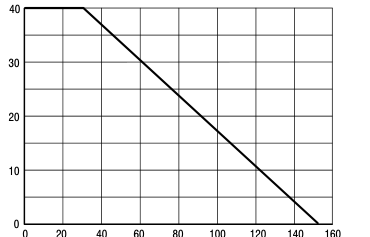
0 20 40 60 80 100 120 140 160
TC, CASE TEMPERATURE (°C)
Figure 1. Power Derating
Page 3
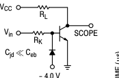
TURN‐ON PULSE APPROX + 11 V
Vin 0 VEB(off)
t1
- 4.0 V
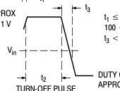
APPROX
t1 ? 7.0 ns
+ 11 V
100 ? t2 ? 500 ?s t3 ? 15 ns
DUTY CYCLE ? 2.0% APPROX - 9.0 V
Figure 2. Switching Time Equivalent Circuit
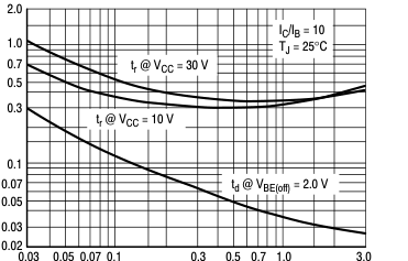
IC, COLLECTOR CURRENT (AMP)
Figure 3. Turn−On Time
t, TIME (ms)
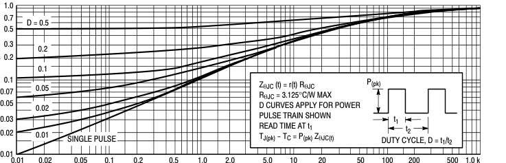
Figure 4. Thermal Response
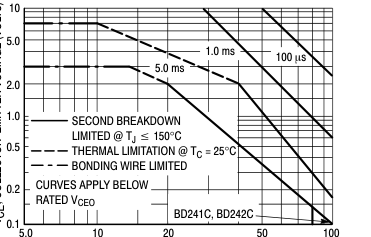
IC, COLLECTOR CURRENT (AMP) Figure 5. Active Region Safe Operating Area
There are two limitations on the power handling ability of
a transistor: average junction temperature and second breakdown. Safe operating area curves indicate IC − VCE
limits of the transistor that must be observed for reliable operation, i.e., the transistor must not be subjected to greater dissipation than the curves indicate.
The data of Figure 5 is based on TJ(pk) = 150°C; TC is
variable depending on conditions. Second breakdown pulse limits are valid for duty cycles to 10% provided TJ(pk)
? 150°C, TJ(pk) may be calculated from the data in
Figure 4. At high case temperatures, thermal limitations will reduce the power that can be handled to values less than the limitations imposed by second breakdown.
Page 4
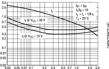
IC, COLLECTOR CURRENT (AMP)
Figure 6. Turn−Off Time
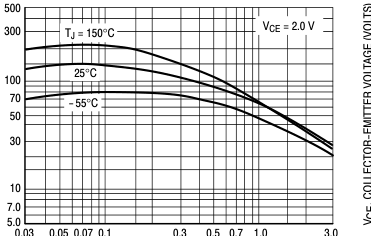
IC, COLLECTOR CURRENT (AMP) Figure 8. DC Current Gain
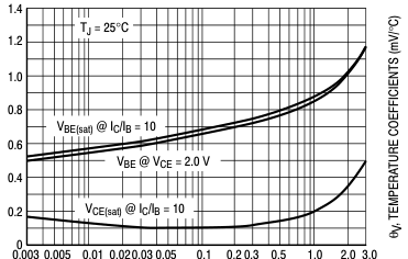
IC, COLLECTOR CURRENT (AMPS) Figure 10. “On” Voltages
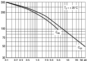
VR, REVERSE VOLTAGE (VOLTS)
Figure 7. Capacitance
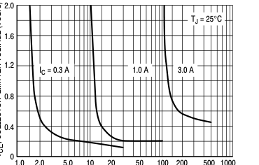
IB, BASE CURRENT (mA) Figure 9. Collector Saturation Region
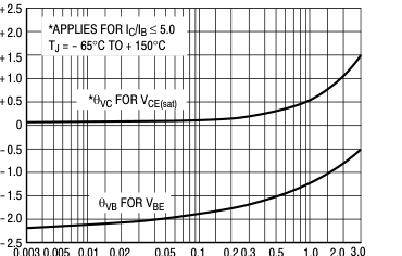
IC, COLLECTOR CURRENT (AMP) Figure 11. Temperature Coefficients
Page 5
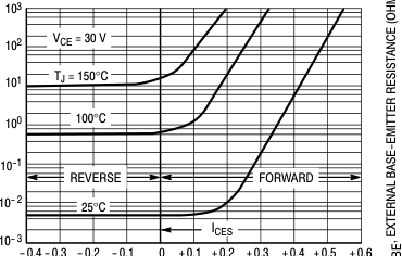
VBE, BASE-EMITTER VOLTAGE (VOLTS) Figure 12. Collector Cut−Off Region
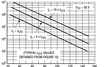
TJ, JUNCTION TEMPERATURE (°C) Figure 13. Effects of Base−Emitter Resistance
Page 6
PACKAGE DIMENSIONS
TO−220
CASE 221A−09
ISSUE AG
NOTES: 1. DIMENSIONING AND TOLERANCING PER ANSI Y14.5M, 1982.
SEATING
−T−
- CONTROLLING DIMENSION: INCH.
PLANE
- DIMENSION Z DEFINES A ZONE WHERE ALL
C
B
F
BODY AND LEAD IRREGULARITIES ARE
| Column 1 | Column 2 |
|---|---|
| 4 Q 1 | B A 2 3 K D |
| H Z L V G |
T
ALLOWED.
S
| Column 1 | Column 2 | Column 3 | Column 4 | Column 5 |
|---|---|---|---|---|
| DIM | INCHES | MILLIMETERS | ||
| MIN | MAX | MIN | MAX | |
| A | 0.570 | 0.620 | 14.48 | 15.75 |
| B | 0.380 | 0.405 | 9.66 | 10.28 |
| C | 0.160 | 0.190 | 4.07 | 4.82 |
| D | 0.025 | 0.036 | 0.64 | 0.91 |
| F | 0.142 | 0.161 | 3.61 | 4.09 |
| G | 0.095 | 0.105 | 2.42 | 2.66 |
| H | 0.110 | 0.161 | 2.80 | 4.10 |
| J | 0.014 | 0.025 | 0.36 | 0.64 |
| K | 0.500 | 0.562 | 12.70 | 14.27 |
| L | 0.045 | 0.060 | 1.15 | 1.52 |
| N | 0.190 | 0.210 | 4.83 | 5.33 |
| Q | 0.100 | 0.120 | 2.54 | 3.04 |
| R | 0.080 | 0.110 | 2.04 | 2.79 |
| S | 0.045 | 0.055 | 1.15 | 1.39 |
| T | 0.235 | 0.255 | 5.97 | 6.47 |
| U | 0.000 | 0.050 | 0.00 | 1.27 |
| V | 0.045 | --- | 1.15 | --- |
| Z | --- | 0.080 | --- | 2.04 |
U
R
J
N
STYLE 1: PIN 1. BASE 2. COLLECTOR 3. EMITTER 4. COLLECTOR

PUBLICATION ORDERING INFORMATION
N. American Technical Support: 800−282−9855 Toll Free
LITERATURE FULFILLMENT:
ON Semiconductor Website: www.onsemi.com
Literature Distribution Center for ON Semiconductor
USA/Canada Europe, Middle East and Africa Technical Support:
Order Literature: http://www.onsemi.com/orderlit
P.O. Box 5163, Denver, Colorado 80217 USA Phone: 303−675−2175 or 800−344−3860 Toll Free USA/Canada
Phone: 421 33 790 2910
For additional information, please contact your local
Japan Customer Focus Center
Fax: 303−675−2176 or 800−344−3867 Toll Free USA/Canada
Sales Representative
Email: orderlit@onsemi.com
Phone: 81−3−5817−1050