

 Download PDF
B3DB3 HARVATEK
Document overview
- PDF pages: 17
Technical content
Page 1
Harvatek Surface Mount CHIP LEDs Data Sheet



| Official Product | HT Part No. B3DB3BRG-05C-000113 | |||
|---|---|---|---|---|
| Tentative Product | **************** | **************** | ||
| Specifications are subject to changes for improvement without advance notice. Proprietary data, drawings, company confidential all rights reserved. | 02/07/2020 | Version 1.0 | Page 1/15 | |
Page 2
DISCLAIMER ......................................................................................................................................... 3 LIFE SUPPORT POLICY ............................................................................................................. 3
PRODUCT SPECIFICATIONS ............................................................................................................. 4
ATTENTION: ELECTROSTATIC DISCHARGE (ESD) PROTECTION ............................................... 4
LABEL SPECIFICATIONS ................................................................................................................... 5
SPECIFICATIONS RANGE .................................................................................................................. 6
PRODUCT FEATURES ......................................................................................................................... 7
ELECTRO-OPTICAL CHARACTERISTICS ...................................................................................... 7 PACKAGE OUTLINE DIMENSION AND RECOMMENDED SOLDERING PATTERN FOR REFLOW
SOLDERING ............................................................................................................................. 7
ELECTRICAL CHARACTERISTICS ................................................................................................. 8 DATA TRANSFER PROTOCOL ..................................................................................................................... 9
PRECAUTION FOR USE .................................................................................................................... 12
PACKAGING ........................................................................................................................................ 13 TAPE DIMENSION ................................................................................................................... 13 REEL DIMENSION ................................................................................................................... 14 PACKING ............................................................................................................................... 14 DRY PACK ............................................................................................................................ 15
BAKING................................................................................................................................. 15 PRECAUTIONS ....................................................................................................................... 15
REFLOW SOLDERING ...................................................................................................................... 16 REWORKING .......................................................................................................................... 16 CLEANING ............................................................................................................................. 16 CAUTIONS OF PICK AND PLACE .............................................................................................. 17 REVISE HISTORY ................................................................................................................... 17
| Official Product | HT Part No. B3DB3BRG-05C-000113 | |||
|---|---|---|---|---|
| Tentative Product | **************** | **************** | ||
| Specifications are subject to changes for improvement without advance notice. Proprietary data, drawings, company confidential all rights reserved. | 02/07/2020 | Version 1.0 | Page 2/15 | |
Page 3
DISCLAIMER
HARVATEK reserves the right to make changes without further notice to any products herein to improve reliability, function or design. HARVATEK does not assume any liability arising out of the application or use of any product or circuit described herein; neither does it convey any license under its patent rights, nor the rights of others.
Life Support Policy HARVATEK’s products are not authorized for use as critical components in life support devices or systems without the express written approval of the President of HARVATEK or HARVATEK INTERNATIONAL. As used herein: 1. Life support devices or systems are devices or systems which, (a) are intended for surgical implant into the body, or (b) support or sustain life, and (c) whose failure to perform when properly used in accordance with instructions for use provided in the labeling, can be reasonably expected to result in a significant injury of the user. 2. A critical component in any component of a life support device or system whose failure to
perform can be reasonably expected to cause the failure of the life support device or system, or to affect its safety or effectiveness.
| Official Product | HT Part No. B3DB3BRG-05C-000113 | |||
|---|---|---|---|---|
| Tentative Product | **************** | **************** | ||
| Specifications are subject to changes for improvement without advance notice. Proprietary data, drawings, company confidential all rights reserved. | 02/07/2020 | Version 1.0 | Page 3/15 | |
Page 4
Product Specifications
| Item | Specification | Material | Quantity |
| Luminous Intensity(Iv) | Red : 40~120 mcd Green : 60~180 mcd Blue : 15~60 mcd IC@5V, R/G/B@5mA Ts= 25O C; Tolerance ±10% | ||
| Wavelength | Red : 618~625 nm Green : 518~535 nm Blue : 460~474 nm IC@5V, R/G/B@5mA Ts= 25O C; Tolerance ±10% | ||
| Applied voltage | 5V_DC | ||
| View angle | 120o | ||
| Resin | Clear | Epoxy | |
| Carrier tape | Conductive black tape | 3000 ea/reel | |
| Reel | Conductive black | ||
| Label | HT standard | Paper | |
| Packing bag | 220x240mm | Aluminum laminated bag/ no-zipper | One reel per bag |
| Carton | HT standard | Paper | Non-specified |
| Others: Each immediate box consists of 5 reels. The 5 reels may not necessarily have the same lot number or the same bin combinations of Iv, λ and Vf. Each reel has a label identifying its specification; the immediate box consists of a product label D as well. Note :This is shipped test conditions ※Remarks: This product should be operated in forward bias. If a reverse voltage is continuously applied to the product, such operation can cause migration resulting in LED damage. ATTENTION: Electrostatic Discharge (ESD) protection The symbol to the left denotes that ESD precaution is needed. ESD protection for GaP and AlGaAs based chips is necessary even though they are relatively safe in the presence of low static-electric discharge. Parts built with AlInGaP, GaN, or/and InGaN based chips are STATIC SENSITIVE devices. ESD precaution must be taken during design and assembly. If manual work or processing is needed, please ensure the device is adequately protected from ESD during the process. | |||
| Official Product | HT Part No. B3DB3BRG-05C-000113 | |||
|---|---|---|---|---|
| Tentative Product | **************** | **************** | ||
| Specifications are subject to changes for improvement without advance notice. Proprietary data, drawings, company confidential all rights reserved. | 02/07/2020 | Version 1.0 | Page 4/15 | |
Page 5
Label Specifications
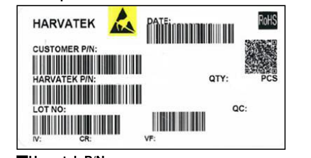
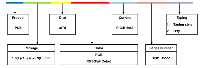
■Harvatek P/N:
B 3DB 3
BRG-
05C- 0001 13
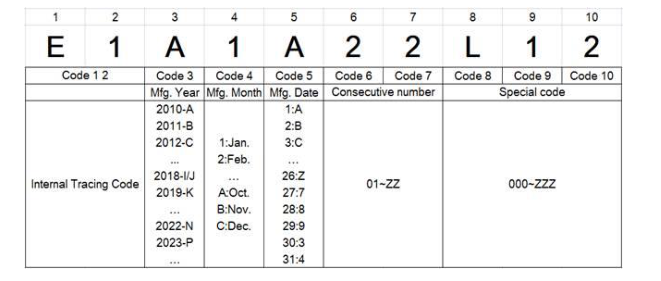
■ Lot No.:
| Official Product | HT Part No. B3DB3BRG-05C-000113 | |||
|---|---|---|---|---|
| Tentative Product | **************** | **************** | ||
| Specifications are subject to changes for improvement without advance notice. Proprietary data, drawings, company confidential all rights reserved. | 02/07/2020 | Version 1.0 | Page 5/15 | |
Page 6
Specifications Range ■Luminous Intensity (Iv) :
| Color | Spec. Range |
| R | 40-120 mcd |
| G | 60-180 mcd |
| B | 15-60 mcd |
Note: It maintains a tolerance of ±10% on luminous intensity
■Wavelength :
| Color | Spec. Range |
| R | 618-625 nm |
| G | 518-535 nm |
| B | 460-474 nm |
Note: It maintains a tolerance of + 0.5nm on Wavelength Bin
| Official Product | HT Part No. B3DB3BRG-05C-000113 | |||
|---|---|---|---|---|
| Tentative Product | **************** | **************** | ||
| Specifications are subject to changes for improvement without advance notice. Proprietary data, drawings, company confidential all rights reserved. | 02/07/2020 | Version 1.0 | Page 6/15 | |
Page 7
Product Features Electro-Optical Characteristics
(TSoldering , 25 oC)
| Series | Emitting Color | Material | Wavelength λ(nm) | I (mcd) V | Viewing Angle 21 2 | ||
| λ D | λ P | △λ | Typical | ||||
| B3DB3BRG | R | AllnGaP | 624 | 630 | 18 | 65 | 120 |
| G | InGaN | 523 | 518 | 35 | 85 | 120 | |
| B | InGaN | 470 | 465 | 25 | 20 | 120 | |
Package Outline Dimension and Recommended Soldering Pattern for Reflow Soldering
(Unit:mm Tolerance: +/-0.1)
| Outline Dim. | Soldering Pattern |
| Soldering terminals may shift in the x, y direction. | |
Absolute Maximum Ratings (unless otherwise specified, Temperature=25°C)
( TSoldering 25 ℃)
| Characteristic | Symbol | Rating | Unit |
|---|---|---|---|
| Supply Voltage | VDD | 6.5 | V |
| Power Dissipation | PD | <400 | mW |
| Maximum Output Current | ILEDOUT | 5 | mA |
| Welding Temperature | TM | 300(8S) | °C |
| Operating Temperature Range | TOPR | -40~85 | °C |
| Storage Temperature Range | TSTO | -65~120 | °C |
| Official Product | HT Part No. B3DB3BRG-05C-000113 | |||
|---|---|---|---|---|
| Tentative Product | **************** | **************** | ||
| Specifications are subject to changes for improvement without advance notice. Proprietary data, drawings, company confidential all rights reserved. | 02/07/2020 | Version 1.0 | Page 7/15 | |
Page 8
Electrical Characteristics
| Characteristic | Symbol | Condition | Limit | Units | ||
|---|---|---|---|---|---|---|
| Min. | Typ. | Max. | ||||
| Supply Voltage | VDD | - | 3.3 | 5.0 | 5.5 | V |
| Operation Current | I dyn | VDD=5V、RGB off | 2 | mA | ||
| Standby Current | I sleep | - | 5 | uA | ||
| Logic input control DIN/CIN | ||||||
| Input High “H” | V IH | - | 2.7 | - | VDD+0.4 | V |
| Input High “L” | V IL | - | -0.4 | - | 1.0 | V |
| DIN Pull-up resistance @normal mode | R IN | 80K | Ω | |||
| CIN Frequency | C FREQ | 15 | MHz | |||
| CIN High pulse width | T CKH | 30 | ns | |||
| CIN Low pulse width | T CKL | 30 | ns | |||
| DIN to CIN setup | T SETUP | 10 | ns | |||
| DIN to CIN hold time | T HOLD | 5 | ns | |||
| Logic output DOUT/COUT | ||||||
| Output High “H” | V OH | 4mA @VDD=5V | 4.5 | - | - | V |
| Output Low “L” | V OL | 4mA @VDD=5V | - | - | 0.4 | V |
| Sink Current R/G/B | ||||||
| R, G, B Sink Current | I SINK | @VDD-Vf ≧1.5V LED | 4.75 | 5 | 5.25 | mA |
| Official Product | HT Part No. B3DB3BRG-05C-000113 | |||
|---|---|---|---|---|
| Tentative Product | **************** | **************** | ||
| Specifications are subject to changes for improvement without advance notice. Proprietary data, drawings, company confidential all rights reserved. | 02/07/2020 | Version 1.0 | Page 8/15 | |
Page 9
Data Transfer Protocol

32 consecutive 0’s denote the start of a command for an RGB LED. After receiving 32 0’s, the IC gets the following 32 bits as the received command, including FLAG, DIMMING, GREEN, BLUE and RED fields.
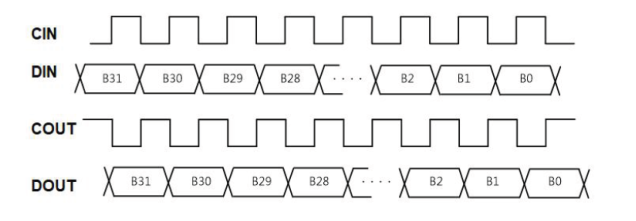
The serial command is transmitted with MSB first, DIN is latched at the rising edge of CIN clock. COUT and DOUT are re-generated for the next RGB LED. COUT is inverted from CIN. When 32 consecutive 0’s are encountered, the next 1 is expected to start a 32-bit command, i.e., FLAG[2:0]=111. When FLAG[2:0]=111, then DIMMING, GREEN, BLUE and RED fields are latched respectively. while the current 32-bit command is got, the IC passes remaining command bits to the next RGB LED.
After the last one command is issued for the last LED (LED n), the following 32 consecutive 1’s denote the end of the current command for an RGB LED(End of Frame) and wait for next 32 consecutive 0’s to start a new command set.(Note: the IC is workable either with or without “End of Frame” command, but MCU should issue the extra N/2 numbers of clocks signal if there are N LED lamps totally connected in the strip to make sure the data transfer and display of the last one LED lamp is complete and correct).

FLAG[2:0] : 111 to start a 32-bit command DIMMING[4:0] : 32-level current control for R/G/B drivers GREEN [7:0] : 256 gray levels for blue LED BLUE [7:0] : 256 gray levels for green LED RED[7:0] : 256 gray levels for red LED
| Official Product | HT Part No. B3DB3BRG-05C-000113 | |||
|---|---|---|---|---|
| Tentative Product | **************** | **************** | ||
| Specifications are subject to changes for improvement without advance notice. Proprietary data, drawings, company confidential all rights reserved. | 02/07/2020 | Version 1.0 | Page 9/15 | |
Page 10
Sleep and power saving mode
The IC supports the sleep/wake-up modes for power-saving purpuse. In sleep mode, the built-in oscillator and associated circuitry will be disabled. The quiencent current of the IC is approximately 1uA(typ.).
Command Setup to enable sleep or wake up mode
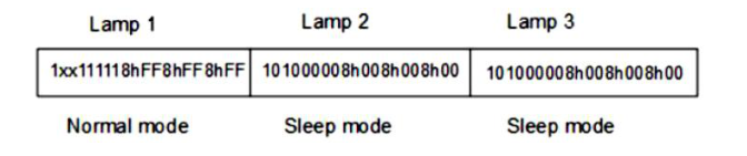
When recieving 24-bit 0’s GBR data (that is GREEN [7:0]=8h00, BLUE [7:0]=8h00, RED[7:0]=8h00), in the meantime, both of the data in 3-bits’ flag and 5-bits’ DIMMING is 8h’A0’ (that is FLAG[2:0]=3b101 and DIMMING[4:0]=5b00000), the IC will enter sleep mode.
The IC will wake up from sleep mode once receiving the new data with the data of Flag[2:0]、 DIMMING[4:0] is not 8h"A0"; after wake-up,all sleeping circuits in the IC return to normal working mode within 1ms. Since it takes 1ms for a sleeping the IC returning to normal function mode, it is recommended for a host to wait for 1ms to send display data and command after issuing a wake-up command.
Sleeep power-saving mode example:

Case 1:
Case 2:
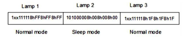
In case 2, while lamp2 is under sleep mode, in the following data transfer process, the state of lamp 2 will be not changed as long as the 32 bits data for lamp 2 is received with data of Flag[2:0]、DIMMING[4:0] being 8h”A0”. It means lamp2 will keep in sleep mode as well. In the situation, lamp2 can pass through the remaining data to
| Official Product | HT Part No. B3DB3BRG-05C-000113 | |||
|---|---|---|---|---|
| Tentative Product | **************** | **************** | ||
| Specifications are subject to changes for improvement without advance notice. Proprietary data, drawings, company confidential all rights reserved. | 02/07/2020 | Version 1.0 | Page 10/15 | |
Page 11
lamp 3 (32bits) to change the display data of lamp 3. In other words, the sleeping chip is able to pass the data to the next chips.
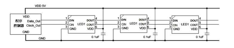
Typical Circuit of an RGB LED strip application
| Official Product | HT Part No. B3DB3BRG-05C-000113 | |||
|---|---|---|---|---|
| Tentative Product | **************** | **************** | ||
| Specifications are subject to changes for improvement without advance notice. Proprietary data, drawings, company confidential all rights reserved. | 02/07/2020 | Version 1.0 | Page 11/15 | |
Page 12
Precaution for Use 1. The chips should not be used directly in any type of fluid such as water, oil, organic solvent, etc. 2. When the LEDs are illuminating, the maximum ambient temperature should be first considered before operation. 3. LEDs must be stored in a clean environment. A sealed container with a nitrogen atmosphere is necessary if the storage period is over 3 months after shipping. 4. The LEDs must be used within 72hours after unpacked. Unused products must be repacked in an anti-electrostatic package, folded to close any opening and then stored in a dry and cool space. 5. The appearance and specifications of the products may be modified for improvement
without further notice. 6. The LEDs are sensitive to the static electricity and surge. It is strongly recommended to use a grounded wrist band and anti-electrostatic glove when handling the LEDs. If a voltage over the absolute maximum rating is applied to LEDs, it will damage LEDs. Damaged LEDs will show some abnormal characteristics such as remarkable increase of leak current, lower turn-on voltage and getting unlit at low current.
| Official Product | HT Part No. B3DB3BRG-05C-000113 | |||
|---|---|---|---|---|
| Tentative Product | **************** | **************** | ||
| Specifications are subject to changes for improvement without advance notice. Proprietary data, drawings, company confidential all rights reserved. | 02/07/2020 | Version 1.0 | Page 12/15 | |
Page 13
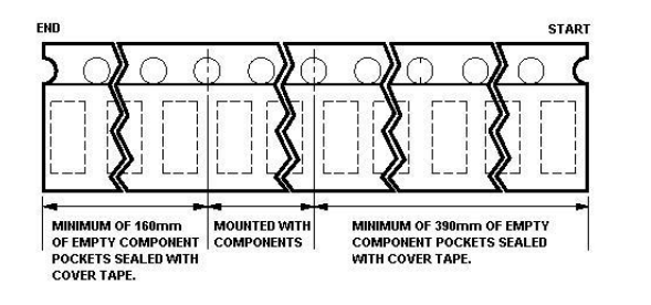
Packaging Tape Dimension
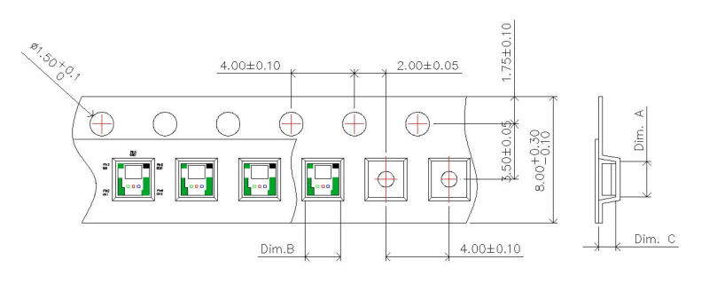
| Dim. A | Dim. B | Dim. C | Q’ty/Reel |
| 1.73±0.05 | 1.73±0.05 | 1.10±0.05 | 3K |
| Official Product | HT Part No. B3DB3BRG-05C-000113 | |||
|---|---|---|---|---|
| Tentative Product | **************** | **************** | ||
| Specifications are subject to changes for improvement without advance notice. Proprietary data, drawings, company confidential all rights reserved. | 02/07/2020 | Version 1.0 | Page 13/15 | |
Page 14
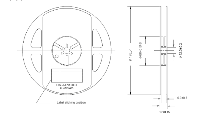
Reel Dimension
Packing
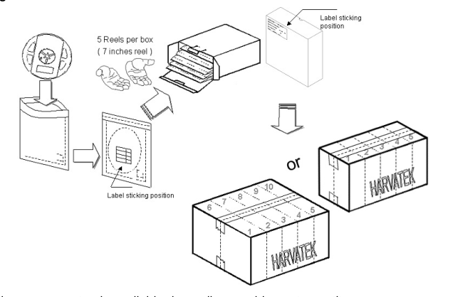
5 or 10 boxes per carton is available depending on shipment quantity.
| Official Product | HT Part No. B3DB3BRG-05C-000113 | |||
|---|---|---|---|---|
| Tentative Product | **************** | **************** | ||
| Specifications are subject to changes for improvement without advance notice. Proprietary data, drawings, company confidential all rights reserved. | 02/07/2020 | Version 1.0 | Page 14/15 | |
Page 15
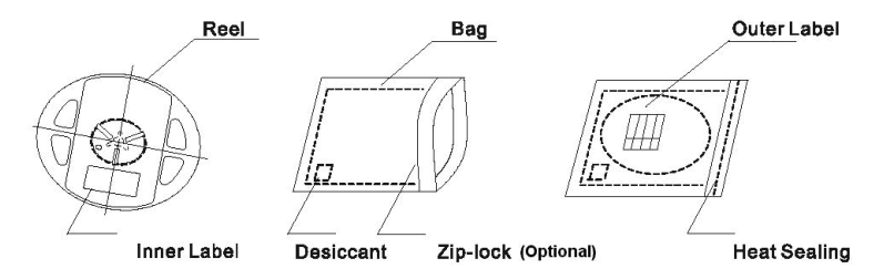
Dry Pack All SMD optical devices are MOISTURE SENSITIVE. Avoid exposure to moisture at all times during transportation or storage. Every reel is packaged in a moisture protected anti-static bag. Each bag is properly sealed prior to shipment.
A humidity indicator will be included in the moisture protected anti-static bag prior to shipment.
The packaging sequence is as follows:
Baking Baking before soldering is recommended when the package has been unsealed for 72hours. The conditions are as followings: 1. 60±3℃×(12~24hrs)and<5%RH, taped reel type. 2. 100±3℃×(45min~1hr), bulk type. 3. 130±3℃×(15min~30min), bulk type. Precautions 1. Avoid exposure to moisture at all times during transportation or storage. 2. Anti-Static precaution must be taken when handling GaN, InGaN, and AlInGaP products. 3. It is suggested to connect the unit with a current limiting resistor of the proper size. Avoid applying a reverse voltage beyond the specified limit. 4. Avoid operation beyond the limits as specified by the absolute maximum ratings. 5. Avoid direct contact with the surface through which the LED emits light.
- If possible, assemble the unit in a clean room or dust-free environment.
| Official Product | HT Part No. B3DB3BRG-05C-000113 | |||
|---|---|---|---|---|
| Tentative Product | **************** | **************** | ||
| Specifications are subject to changes for improvement without advance notice. Proprietary data, drawings, company confidential all rights reserved. | 02/07/2020 | Version 1.0 | Page 15/15 | |
Page 16
Reflow Soldering Recommend soldering paste specifications: 1. Operating temp.: Above 220℃ ,60 sec. 2. Peak temp.:260 ℃Max.,10sec Max. 3. Reflow soldering should not be done more than two times. 4. Never attempt next process until the component is cooled down to room temperature after reflow. 5. The recommended reflow soldering profile (measured on the surface of the LED terminal) is as following: Lead-free Solder Profile
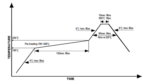
Reworking Rework should be completed within 5 seconds under 260 ℃. The iron tip must not come in contact with the copper foil. Twin-head type is preferred.
Cleaning Following are cleaning procedures after soldering: An alcohol-based solvent such as isopropyl alcohol (IPA) is recommended. Temperature x Time should be 50℃ x 30sec. or <30℃ x 3min Ultrasonic cleaning: < 15W/ bath; bath volume ≤ 1liter Curing: 100 ℃ max, <3min
| Official Product | HT Part No. B3DB3BRG-05C-000113 | |||
|---|---|---|---|---|
| Tentative Product | **************** | **************** | ||
| Specifications are subject to changes for improvement without advance notice. Proprietary data, drawings, company confidential all rights reserved. | 02/07/2020 | Version 1.0 | Page 16/15 | |
Page 17
Cautions of Pick and Place Avoid stress on the resin at elevated temperature. Avoid rubbing or scraping the resin by any object. Electric-static may cause damage to the component. Please ensure that the equipment is properly grounded. Use of an ionizer fan is recommended.
Revise History
| Official Product | HT Part No. B3DB3BRG-05C-000113 | |||
|---|---|---|---|---|
| Tentative Product | **************** | **************** | ||
| Specifications are subject to changes for improvement without advance notice. Proprietary data, drawings, company confidential all rights reserved. | 02/07/2020 | Version 1.0 | Page 17/15 | |