

 Download PDF
B120/B - B160/B
Document overview
- PDF pages: 6
Technical content
Page 1
1.0A SURFACE-MOUNT SCHOTTKY BARRIER RECTIFIER
Product Summary
B120/B, B130/B, B140/B
| VRRM (V) | IO (A) | VF Max (V) TA = +25°C | IR Max (mA) TA = +25°C |
|---|---|---|---|
| 20/30/40 | 1.0 | 0.5 | 0.5 |
B150/B, B160/B
| VRRM (V) | IO (A) | VF Max (V) TA = +25°C | IR Max (mA) TA = +25°C |
|---|---|---|---|
| 50/60 | 1.0 | 0.7 | 0.5 |
Description and Applications
This Schottky barrier rectifier is designed to meet the general requirements of commercial applications. It is ideally suited for use as:
Polarity protection diodes Re-circulating diodes Switching diodes
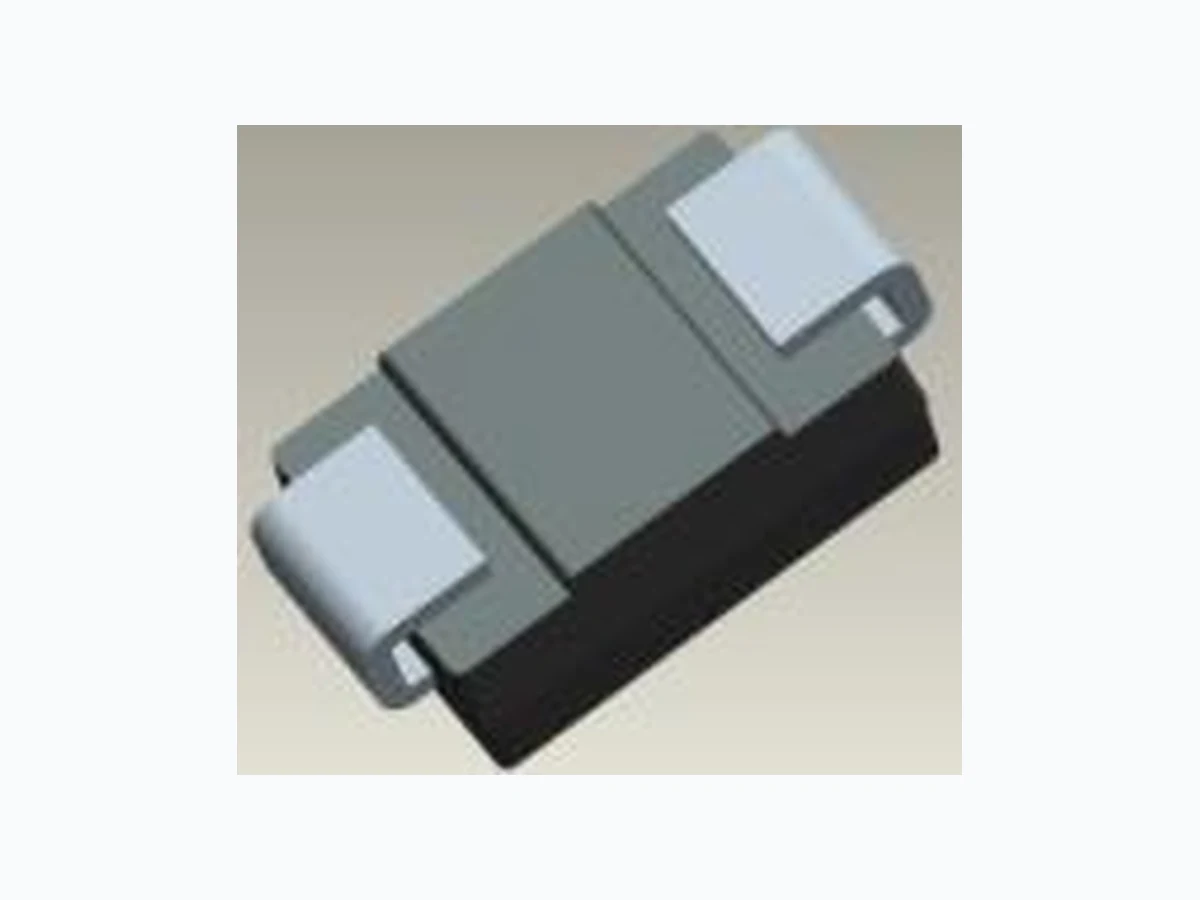
Top View
Ordering Information (Note 4)
Features and Benefits
Guard Ring Die Construction for Transient Protection Ideally Suited for Automated Assembly Low Power Loss, High Efficiency Surge Overload Rating to 30A Peak For Use in Low-Voltage, High-Frequency Inverters, Free Wheeling, and Polarity Protection Application Lead-Free Finish; RoHS Compliant (Notes 1 & 2) Halogen and Antimony Free. “Green” Device (Notes 3) For automotive applications requiring specific change control (i.e. parts qualified to AEC-Q100/101/104/200, PPAP capable, and manufactured in IATF 16949 certified facilities), please contact us or your local Diodes representative. https://www.diodes.com/quality/product-definitions/
Mechanical Data
Package: SMA/SMB Package Material: Molded Plastic. UL Flammability Classification Rating 94V-0 Moisture Sensitivity: Level 1 per J-STD-020 Terminals: Lead Free Plating (Matte Tin Finish). Solderable per MIL-STD-202, Method 208 Polarity: Cathode Band or Cathode Notch Weight: SMA 0.064 grams (Approximate) SMB 0.093 grams (Approximate)
Bottom View
| Part Number | Package | Packing | |
| Qty. | Carrier | ||
| B1XX-13-F | SMA | 5,000 | Tape & Reel |
| B1XXB-13-F | SMB | 3,000 | Tape & Reel |
\*XX = Device Type, e.g., B120-13-F (SMA Package); B120B-13-F (SMB Package). Notes: 1. EU Directive 2002/95/EC (RoHS), 2011/65/EU (RoHS 2) & 2015/863/EU (RoHS 3) compliant. All applicable RoHS exemptions applied. 2. See https://www.diodes.com/quality/lead-free/ for more information about Diodes Incorporated’s definitions of Halogen- and Antimony-free, "Green" and Lead-free. 3. Halogen- and Antimony-free "Green” products are defined as those which contain <900ppm bromine, <900ppm chlorine (<1500ppm total Br + Cl) and <1000ppm antimony compounds. 4. For packaging details, go to our website at https://www.diodes.com/design/support/packaging/diodes-packaging/.
Marking Information
B1X0 = Product Type Marking Code, e.g., B120 (SMA Package)
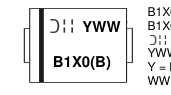
B1X0B = Product Type Marking Code, e.g., B160B (SMB Package) = Manufacturers’ Code Marking YWW = Date Code Marking Y = Last Digit of Year (ex: 3 for 2023) WW = Week Code (01 to 53)
1 of 6
Page 2
Maximum Ratings (@TA = +25°C, unless otherwise specified.)
Single phase, half wave, 60Hz, resistive or inductive load For capacitive load, derate current by 20%.
| Characteristic | Symbol | B120/B B130/B | B140/B B150/ | B B160/B | Unit |
|---|---|---|---|---|---|
| Peak Repetitive Reverse Voltage Working Peak Reverse Voltage DC Blocking Voltage | VRRM VRWM VR | 20 30 | 40 50 | 60 | V |
| RMS Reverse Voltage | VR(RMS) | 14 21 | 28 35 | 42 | V |
| Average Rectified Output Current @ TT = +130°C | IO | 1.0 | A | ||
| Non-Repetitive Peak Forward Surge Current 8.3ms Single Half Sine Wave Superimposed on Rated Load | IFSM | 30 | A | ||
Thermal Characteristics
| Characteristic | Symbol | B120/B B130/B | B140/B B150/ | B B160/B | Unit |
|---|---|---|---|---|---|
| Typical Thermal Resistance Junction to Terminal (Note 5) | RJT | 20 | °C/W | ||
| Operating and Storage Temperature Range | TJ, TSTG | -65 to +150 | °C | ||
Electrical Characteristics (@TA = +25°C, unless otherwise specified.)
| Characteristic | Symbol | Min Typ | Max Unit | Test Condition |
|---|---|---|---|---|
| B120/B, B130/B, B140/B Forward Voltage Drop B150/B, B160/B | VF | — — — — | 0.5 IF V 0.7 IF | = 1.0A = 1.0A |
| Leakage Current (Note 6) | IR | — — — — | 0.5 @ mA 10 @ | Rated VR, TA = +25°C Rated VR, TA = +100°C |
| Total Capacitance | CT | — 110 | — pF V | R = 4V, f = 1MHz |
Notes: 5. Thermal Resistance: Junction to terminal, unit mounted on PC board with 5.0mm2 (0.013mm thick) copper pads as heat sink. 6. Short duration pulse test used to minimize self-heating effect.
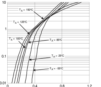
V , INSTANTANEOUS FORWARD VOLTAGE (V) F Figure 1. Figure 1 Typical Forward Characteristics
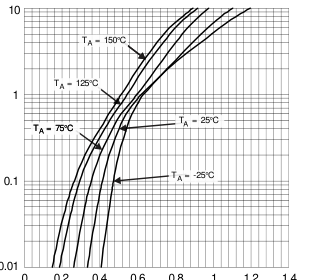
0 0.2 0.4 0.6 0.8
1 1.2 1.4
V , INSTANTANEOUS FORWARD VOLTAGE (V) F Figure 2. Figure 2 Typical Forward Characteristics B150/B through B160/B
2 of 6
Page 3
10000
0 10 20 30 40 50
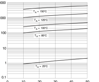
V , INSTANTANEOUS REVERSE VOLTAGE (V) R Figure 3. Figure 3 Typical Reverse Characteristics B120/B through B140/B
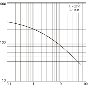
V , DC REVERSE VOLTAGE (V) R Figure 5. Fig. 5 Total Capacitance vs. Reverse Voltage
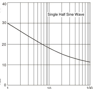
NUMBER OF CYCLES AT 60 Hz
Figure 7. Fig. 7 Max Non-Repetitive Peak Forward Surge Current
3 of 6 10000
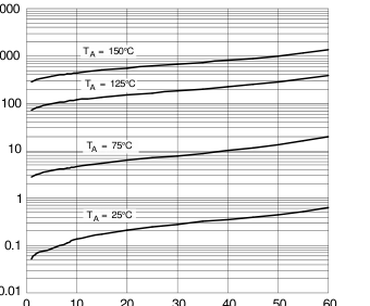
V , INSTANTANEOUS REVERSE VOLTAGE (V) R Figure 4. Figure 4 Typical Reverse Characteristics B150/B through B160/B
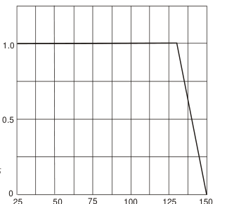
(°C)
T , TERMINAL TEMPERATURE (篊 ) T Figure 6. Fig. 6 Forward Current Derating Curve
Page 4
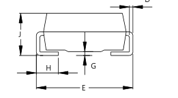
Package Outline Dimensions
Please see http://www.diodes.com/package-outlines.html for the latest version.
SMA
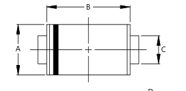
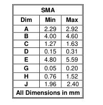
D
SMB
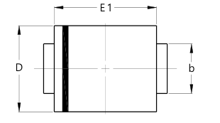
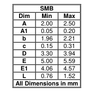
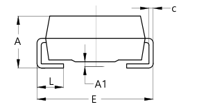
4 of 6
Page 5
Suggested Pad Layout
Please see http://www.diodes.com/package-outlines.html for the latest version.
SMA
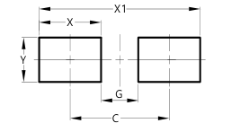
| Dimensions | Value (in mm) |
| C | 4.00 |
| G | 1.50 |
| X | 2.50 |
| X1 | 6.50 |
| Y | 1.70 |
SMB
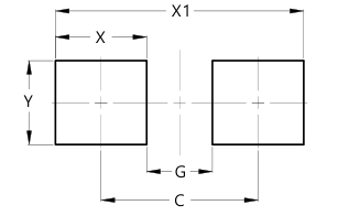
| Dimensions | Value (in mm) |
| C | 4.30 |
| G | 1.80 |
| X | 2.50 |
| X1 | 6.80 |
| Y | 2.30 |
5 of 6
Page 6
IMPORTANT NOTICE
DIODES INCORPORATED (Diodes) AND ITS SUBSIDIARIES MAKE NO WARRANTY OF ANY KIND, EXPRESS OR IMPLIED, WITH 1. REGARDS TO ANY INFORMATION CONTAINED IN THIS DOCUMENT, INCLUDING, BUT NOT LIMITED TO, THE IMPLIED WARRANTIES OF MERCHANTABILITY, FITNESS FOR A PARTICULAR PURPOSE OR NON-INFRINGEMENT OF THIRD PARTY INTELLECTUAL PROPERTY RIGHTS (AND THEIR EQUIVALENTS UNDER THE LAWS OF ANY JURISDICTION).
The Information contained herein is for informational purpose only and is provided only to illustrate the operation of Diodes’ products 2. described herein and application examples. Diodes does not assume any liability arising out of the application or use of this document or any product described herein. This document is intended for skilled and technically trained engineering customers and users who design with Diodes’ products. Diodes’ products may be used to facilitate safety-related applications; however, in all instances customers and users are responsible for (a) selecting the appropriate Diodes products for their applications, (b) evaluating the suitability of Diodes’ products for their intended applications,
(c) ensuring their applications, which incorporate Diodes’ products, comply the applicable legal and regulatory requirements as well as safety and functional-safety related standards, and (d) ensuring they design with appropriate safeguards (including testing, validation, quality control techniques, redundancy, malfunction prevention, and appropriate treatment for aging degradation) to minimize the risks associated with their applications.
Diodes assumes no liability for any application-related information, support, assistance or feedback that may be provided by Diodes 3. from time to time. Any customer or user of this document or products described herein will assume all risks and liabilities associated with such use, and will hold Diodes and all companies whose products are represented herein or on Diodes’ websites, harmless against all damages and liabilities.
Products described herein may be covered by one or more United States, international or foreign patents and pending patent 4. applications. Product names and markings noted herein may also be covered by one or more United States, international or foreign trademarks and trademark applications. Diodes does not convey any license under any of its intellectual property rights or the rights of any third parties (including third parties whose products and services may be described in this document or on Diodes’ website) under this document.
- Diodes’ products are provided subject to
Diodes’ Standard Terms and Conditions of Sale
(https://www.diodes.com/about/company/terms-and-conditions/terms-and-conditions-of-sales/) or other applicable terms. This document does not alter or expand the applicable warranties provided by Diodes. Diodes does not warrant or accept any liability whatsoever in respect of any products purchased through unauthorized sales channel.
Diodes’ products and technology may not be used for or incorporated into any products or systems whose manufacture, use or sale is 6. prohibited under any applicable laws and regulations. Should customers or users use Diodes’ products in contravention of any applicable laws or regulations, or for any unintended or unauthorized application, customers and users will (a) be solely responsible for any damages, losses or penalties arising in connection therewith or as a result thereof, and (b) indemnify and hold Diodes and its representatives and agents harmless against any and all claims, damages, expenses, and attorney fees arising out of, directly or indirectly, any claim relating to any noncompliance with
the applicable laws and regulations, as well as any unintended or unauthorized application.
While efforts have been made to ensure the information contained in this document is accurate, complete and current, it may contain 7. technical inaccuracies, omissions and typographical errors. Diodes does not warrant that information contained in this document is error-free and Diodes is under no obligation to update or otherwise correct this information. Notwithstanding the foregoing, Diodes reserves the right to make modifications, enhancements, improvements, corrections or other changes without further notice to this document and any product described herein. This document is written in English but may be translated into multiple languages for reference. Only the English version of this document
is the final and determinative format released by Diodes.
Any unauthorized copying, modification, distribution, transmission, display or other use of this document (or any portion hereof) is 8. prohibited. Diodes assumes no responsibility for any losses incurred by the customers or users or any third parties arising from any such unauthorized use.
- This Notice may be periodically updated with the most recent version available at https://www.diodes.com/about/company/terms-andconditions/important-notice
The Diodes logo is a registered trademark of Diodes Incorporated in the United States and other countries. All other trademarks are the property of their respective owners. © 2023 Diodes Incorporated. All Rights Reserved.
6 of 6