
 Download PDF
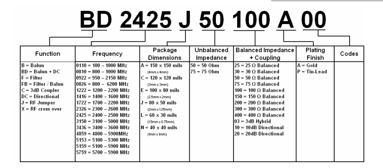
B0011E75300A00 ANAREN
Document overview
- PDF pages: 10
Technical content
Page 1

Ultra Low Profile 1008 Balun
75Ω to 300Ω Balanced
Description
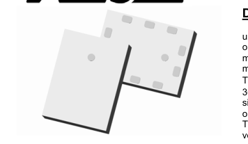
The B0011E75300A00 is a low profile sub-miniature balanced to unbalanced transformer designed for differential inputs and output locations on next generation analog and digital TV chipsets in an easy to use surface mount package.
The B0011E75300A00 is ideal for high volume
manufacturing and is higher performance than traditional wire wound baluns. The B0011E75300A00 has an unbalanced port impedance of 75Ω and a 300Ω balanced port impedance. This transformation enables single ended signals to be applied to differential ports on modern semiconductors. The output ports have equal amplitude (-3dB) with 180 degree phase differential. The B0011E75300A00 is available on tape and reel for pick and place high volume manufacturing.
Detailed Electrical Specifications: Specifications subject to change without notice.
| Features: • 48 – 1080 MHz • 1.0 mm Height Profile • 75 Ohm to 2 x 150 Ohm • DVB-T, DVB-H and DVB-C • Low Insertion Loss • Surface Mountable • Tape & Reel • Non-conductive Surface • RoHS Compliant | Parameter | ROOM (25°C) Min. Typ. Max | Unit |
|---|---|---|---|
| Frequency Unbalanced Port Impedance Balanced Port Impedance Return Loss Insertion Loss* Amplitude Balance Phase Balance CMRR Power Handling Operating Temperature | 48 1080 75 300 9 11 1.3 1.6 0.6 1.5 6 15 28 TBD -55 +85 | MHz Ω Ω dB dB dB Degrees dB Watts ºC |
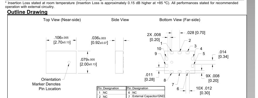
| 2 | NC | 7 | External Capacitor/GND |
| 3 | NC | 8 | NC |
| 4 | Unbalanced Port | 9 | Balanced Port 1 |
| 5 | GND | 10 | Balanced Port 2 |
Dimensions are in Inches [Millimeters] Mechanical Outline
Page 2
Typical Performance with Two External 82pF Capacitors (test/specification condition)
| 11 ZO=P 7o 5r Ωt_ [1 =Zin] C=C 822 pF 4 10 ZO=15P 0o Ωrt [_ =3 Zout/2] 4 7 3 3 B0011E75300Axx R1 6 6 R=300Ω [Zout] 5 2 1 1 7 C1 Port_2 C=82pF ZO=150Ω [=Zout/2] 5 12 9 Figure 1 The Balun with external capacitors on both low impedance ports (nominal/test configuration). The two capacitors improve the insertion loss and return loss in the 40-200MHz range over that of the basic balun. Amplitude Balance | Insertion Loss 82pF series capacitors on Pin 4&7 0 48MHz 57MHz 170MHz 870MHz 1080MHz -0.3 -0.519 -0.6 -0.9 -1.014 -1.108 -1.2 -1.381 -1.343 -1.5 Loss -1.8 Insertion -2.1 -2.4 -2.7 -3 -3.3 -3.6 100 1000 FFrreeqquueennccyy ((MMHHzz)) Return Loss |
|---|---|
| 82pF series capacitors on Pin 4&7 2 48MHz 57MHz 170MHz 870MHz 1080MHz 1.6 1.2 0.8 0.559 0.4 0.255 Balance 0 -0.072 Amplitude -0.4 -0.483 -0.76 -0.8 -1.2 -1.6 -2 100 1000 FFrreeqquueennccyy ((MMHHzz)) | 82pF series capacitors on Pin 4&7 0 48MHz 57MHz 170MHz 870MHz 1080MHz -3 -6 -9 -12 -13.60- 511.975 -14.55 -15 Loss -18 -18.969 Return -21 -24 -24.202 -27 -30 -33 -36 100 1000 FFrreeqquueennccyy ((MMHHzz)) |
| Phase Balance (Delta 180) 82pF series capacitors on Pin 4&7 20 48MHz 57MHz 170MHz 870MHz 1080MHz 16 12 8 8.077 4.712 180) 4 2.1182.293 1.891 (Delta 0 Balance -4 Phase -8 -12 -16 -20 100 1000 FFrreeqquueennccyy ((MMHHzz)) | Common Mode Rejection 82pF series capacitors on Pin 4&7 0 48MHz 57MHz 170MHz 870MHz 1080MHz -3 -6 -9 -12 Rejection -15 -18 Mode -21 -21.614 Common -24 -26.079 -27 -28.613 -30 -32.109 -33 -35.381 -36 100 1000 FFrreeqquueennccyy ((MMHHzz)) |
Page 3

Typical Performance with One External 82pF Capacitor
| 11 4 10 ZO=15P 0o Ωrt [_ =3 Zout/2] 4 Port_1 ZO=75Ω [=Zin] 3 3 B0011E75300Axx R1 6 6 R=300Ω [Zout] 5 2 1 1 7 C1 Port_2 C=82pF ZO=150Ω [=Zout/2] 5 12 9 Figure 2 The Balun with an external capacitor on the low impedance ground pin. This improves insertion loss and return loss in the 40-200MHz range over that of the basic configuration. The capacitor value can be changed some to get a slightly different performance. A series capacitor with just pin 4 does NOT produce identical results as the one just in series with pin 7. | Insertion Loss 82pF series capacitor on Pin 7 0 48MHz 57MHz 170MHz 870MHz 1080MHz -0.3 -0.497 -0.6 -0.9 -0.962 -1.2 -1.232 -1.308 -1.5 -1.661 Loss -1.8 Insertion -2.1 -2.4 -2.7 -3 -3.3 -3.6 100 1000 FFrreeqquueennccyy ((MMHHzz)) Return Loss |
| Amplitude Balance 82pF series capacitor on Pin 7 2 48MHz 57MHz 170MHz 870MHz 1080MHz 1.6 1.2 0.8 0.587 0.4 0.283 Balance 0 -0.015 -0.283 Amplitude -0.4 -0.614 -0.8 -1.2 -1.6 -2 100 1000 FFrreeqquueennccyy ((MMHHzz)) | 82pF series capacitor on Pin 7 0 48MHz 57MHz 170MHz 870MHz 1080MHz -3 -6 -9 -10.9-9191.577 -12 -12.417 -14.678 -15 Loss -18 -18.631 Return -21 -24 -27 -30 -33 -36 100 1000 FFrreeqquueennccyy ((MMHHzz)) |
| Phase Balance (Delta 180) 82pF series capacitor on Pin 7 20 48MHz 57MHz 170MHz 870MHz 1080MHz 16 12 8 6.305 180) 4 1.9962.147 2.108 3.206 (Delta 0 Balance -4 Phase -8 -12 -16 -20 100 1000 FFrreeqquueennccyy ((MMHHzz)) | Common Mode Rejection 82pF series capacitor on Pin 7 0 48MHz 57MHz 170MHz 870MHz 1080MHz -3 -6 -9 -12 Rejection -15 -18 Mode -21 Common -23.683 -24 -27 -28.399 -29.797 -30 -32.098 -33 -34.696 -36 100 1000 FFrreeqquueennccyy ((MMHHzz)) |
Page 4
Typical Performance with no External Components
| 11 10 Port_3 4 4 ZO=150Ω [=Zout/2] Port_1 ZO=75Ω [=Zin] 3 3 B0011E75300Axx R1 6 6 R=300Ω [Zout] 5 1 1 7 Port_2 ZO=150Ω [=Zout/2] 5 12 9 Figure 3 The Balun in it’s basic configuration with no external components. | Insertion Loss No External Components 0 48MHz 57MHz 170MHz 870MHz 1080MHz -0.3 -0.583 -0.6 -0.9 -0.974 -1.2 -1.399 -1.5 Loss -1.8 Insertion -2.1 -2.4 -2.47 -2.7 -3 -3.115 -3.3 -3.6 100 1000 FFrreeqquueennccyy ((MMHHzz)) Return Loss |
| Amplitude Balance No External Components 2 48MHz 57MHz 170MHz 870MHz 1080MHz 1.6 1.2 0.8 0.4 Balance 0 -0.08-40.08 -1.042e-3 Amplitude -0.358 -0.4 -0.553 -0.8 -1.2 -1.6 -2 100 1000 FFrreeqquueennccyy ((MMHHzz)) | No External Components 0 48MHz 57MHz 170MHz 870MHz 1080MHz -3 -4.145 -5.039 -6 -9 -11.154 -12 -14.713 -14.226 -15 Loss -18 Return -21 -24 -27 -30 -33 -36 100 1000 FFrreeqquueennccyy ((MMHHzz)) |
| Phase Balance (Delta 180) No External Components 20 48MHz 57MHz 170MHz 870MHz 1080MHz 16 12 8 5.796 180) 4 2.5032.253 1.85 2.698 (Delta 0 Balance -4 Phase -8 -12 -16 -20 100 1000 FFrreeqquueennccyy ((MMHHzz)) | Common Mode Rejection No External Components 0 48MHz 57MHz 170MHz 870MHz 1080MHz -3 -6 -9 -12 Rejection -15 -18 Mode -21 Common -24 -24.469 -27 -30 -30.093 -33.006 -33 -33.897 -35.838 -36 100 1000 FFrreeqquueennccyy ((MMHHzz)) |
Page 5

Additional Configurations
| 11 4 10 ZO=15P 0o Ωrt _ [=3 Zout/2] 4 Port_1 ZO=75Ω [=Zin] 3 3 B0011E75300Axx R1 6 6 R=300Ω [Zout] 5 2 L1 1 1 7 L=2.4nH Port_2 ZO=150Ω [=Zout/2] 5 12 9 Figure 4 The balun with an external inductor in the low impedance ground path. This improves the insertion loss, return loss and balanced performance in the 870-1080MHz range. This inductance can be realized as a transmission line (dimensions will depend on the PCB material and ground plane distance). The added inductance can be used in conjunction with the external capacitors. When mounted with high groundplane spacing, part of this inductance comes automatically from the increased inductance of the typical via to ground. | 11 11 ZO=P 7o 5r Ωt_ [1 =Zin] C=C 821 pF 4 10 ZO=15P 0o Ωrt _ [=3 Zout/2] 4 2 8 8 B0011E75300Axx R1 13 R=300Ω [Zout] 5 3 1 1 C2 7 Port_2 C=82pF ZO=150Ω [=Zout/2] 5 12 12 9 SG1 VDC=V [Bias Voltage] 13 13 13 100mA max C3 C4 C=3900pF C=82pF 9 9 9 Figure 5 Biasing the balanced signals thru the balun. Dependign on the quality of “C3” the additional capacitor “C4” may not be needed. The DC-resistance from the bias point thru to each of the outputs are 10±4Ω. It is important to keep inductance to a minimum from pin 5 to ground or balanced performance will suffer. When used with high groundplane spacings it is recommended to have two or more via to ground. |
|---|---|
| 11 11 ZO=P 7o 5r Ωt_ [1 =Zin] C=C 81 2pF 4 10 ZO=15P 0o Ωrt _ [=3 Zout/2] 4 2 6 6 B0011E75300Axx R1 1 R=300Ω [Zout] 5 3 3 7 5 12 12 9 Figure 6 Using the balun as an single ended to single ended impedance transformer (Unun). Pin 5 must be open circuit. It is recommended to use the 82pF on the low impedance side to improve the insertion loss and return loss in the 50-200MHz range. Note that pins 4 & 7 can only be interchanged if pins 9 7 10 are also interchanged, otherwise performance will suffer. | |
Page 6
Distortion Considerations:
This balun does NOT contain any ferrite materials and are as such distortion free. Very, very low levels of distortion can arise from dissimilar metals on the contact pads of the part (Cu-Ni-Au) and from inter-metallic contaminations within the part.
Power Handling Considerations:
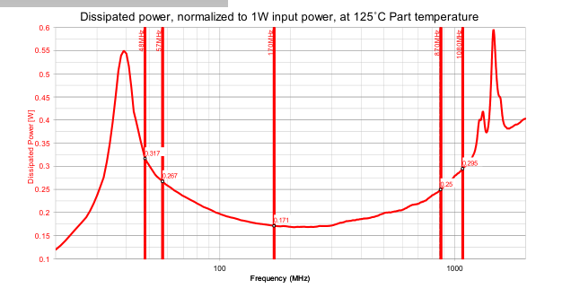
The RF-power handling capability of these baluns depends on the temperature at the mounted interface (base plate temperature), and whether or not DC-bias is feed through the part. The power handling specified is for a mounted temperature of 85˚C and no DC-bias and is based on a maximum operating temperature of the part itself of 125˚C (do not exceed this).
The maximum power handling relates to the dissipated power within the part and is therefore a function of insertion loss. The insertion loss of this device changes within the specified band. Thus if operated with a narrowband signal at either band edge (this is what is specified) it will have less power handling than if operated closer to the center of the band or if operated with a very wideband signal. If signals arrive at the balun that are out of the specified band, these must be included in the total dissipated power calculation. However the deteriorating return loss will eliminate some of this power.
The dissipated RF power can be estimated as;
RL
IL
dB
dB
−
−
= P 1−10
1−10 10
10
[W ]
P
RF ,diss in
Where:
- P is the input power, either on the low impedance side, single ended or the combined differential power in
on the balanced side, depending on the feeding direction.
- RL is the return loss in dB associated with the feeding port. I.e. if feed from the balanced side then the
dB balanced return loss must be used (this however is very similar to the single ended return loss). is the insertion loss at the operating temperature of the device.
- ILdB
Below the dissipated power is shown at a normalized 1W input power for the balun internal temperature of 125˚C.
Page 7

When used with DC-biasing the RF-power must be de-rated with the amount of DC power dissipated; (
)
P = R || R I ≈ 7I [W
2 2 ]
dc,diss out1 out 2 dc
dc
The total dissipated power cannot exceed TBD.
When the duty cycle is not 100% the input power can be averaged, however the instantaneous input power should newer exceed TBD.
Page 8
Mounting Configuration:
In order for Xinger surface mount components to work optimally, the proper impedance transmission lines must be used to connect to the RF ports. If this condition is not satisfied, insertion loss, Isolation and VSWR may not meet published specifications.
All of the Xinger components are constructed from softboard composites which possess excellent electrical and mechanical stability having X and Y thermal coefficient of expansion (CTE) of 19 ppm/oC.
An example of the PCB footprint used in the testing of these parts is shown below. In specific designs, the transmission line widths need to be adjusted to the unique dielectric coefficients and thicknesses as well as varying pick and place equipment tolerances.
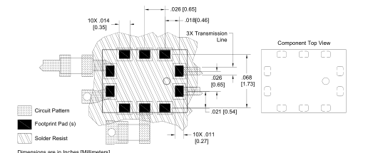
Dimensions are in Inches [Millimeters] Mounting Footprint
The material used for testing is 8mil Rogers 4003. For a ground plane spacing much larger than this the single via at pin 5 should be replaced with at least 2 via and if possible a coplanar ground.
Page 9

Packaging and Ordering Information
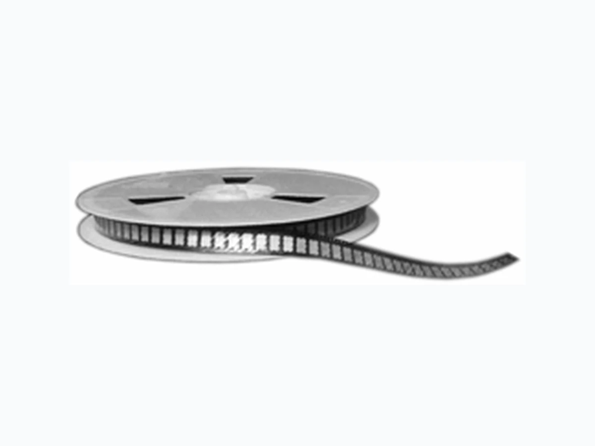
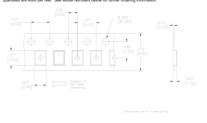
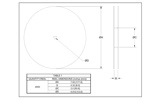
Parts are available in reel and are packaged per EIA 481-2. Parts are oriented in tape and reel as shown below. Minimum order
quantities are 4000 per reel. See Model Numbers below for further ordering information.
Page 10