

 Download PDF
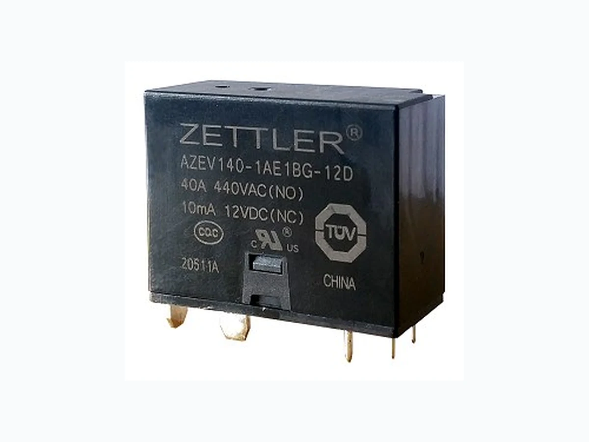
AZEV140 AZETTLER
Document overview
- Manufacturer or author: Provided By digicamel.com
- PDF pages: 4
Technical content
www.ZETTLER-group.com page 1 of 4 2024-04-29 Arrangement load contact signal contact SPST-NO (1 Form A) SPST-NC (1 Form B) coupled to NO load contact Ratings (max.) load contact switched power switched current continuous current switched voltage contact load category signal contact switched current minimum load (resistive load) 22000 VA 50 A 50 A
440 VAC
10 mA, 5 VDC, 50mW (gold plated contact) Approved ratings load contact signal contact (UL/CUR/TÜV/CQC)
40 A at 440 VAC, resistive, 85°C, 30k cycles
32 A at 440 VAC, resistive, 85°C, 50k cycles
50 A at 440 VAC, resistive, 85°C, 6k cycles
20 A make, 50 A carry, 20 A break at 440 VAC,
resistive, 85°C, 50k cycles 10 mA at 12 VDC, 85°C, 50k cycles Contact material load contact signal contact AgSnO2 (silver tin oxide) AgNi + Au (silver nickel, gold plated) Contact gap load contact (clearance of open load contacts) ≥ 2.25 mm Contact resistance load contact initial typical ≤ 50 mΩ (at 6VDC/1A) ≤ 3 mΩ (at 40 A, contact factory for details) CONTACTS Life Expectancy mechanical electrical (minimum operations) 1 x 10⁵ see UL/CUR/TÜV/CQC approved ratings Timing operate time release time (at nominal coil voltage) ≤ 30 ms ≤ 10 ms (without coil suppression) Dielectric Strength open load contacts coil to load contacts open signal contacts coil to signal contacts signal to load contacts (at sea level for 1 min.)
2500 VRMS
4000 VRMS
500 VRMS
(clearance / creepage) ≥ 2.25 mm / ≥ 4.2 mm Insulation Resistance 1000 MΩ (min.) at 23°C, 500 VDC, 50% RH Pulse current capability ≥ 1.50 kA , ≥ 6.0 kA²s (based on requirements of IEC 62752) ≥ 1.85 kA , ≥ 4.5 kA²s (based on requirements of IEC 62955) Temperature Range operating (at nominal coil voltage) Vibration resistance 0.062" (1.5 mm) DA at 10–55 Hz Enclosure protection category material material group Flammability RT II, flux proof PBT. polyester IIIa UL94 V-0 Terminals Tinned copper alloy, THT PCB mounting Soldering preheating soldering (referring IEC 61760-1 wave soldering) Dimensions and Weight 35 mm x 16 mm x 28 mm, 35 grams Compliance UL 508, IEC 61810-1, GB/T 21711.1-2008 RoHS, REACH designed to meet requirements of IEC 62752 Agency Approvals UL / CUR TÜV CQC E365652 B 088793 0016 CQC20002276475 Packing (pcs.) 50 per plastic tray 400 per carton box GENERAL DATA
FEATURES
- Designed for IEC 61851 Mode 2 charging applications
- NO load contact plus NC signal contact for welding monitoring
- 40 Amp nominal, up to 50 Amp switching capability
- Electrical ratings according IEC 61851-1: CC2 / 50.000 cycles
- Withstands up to 1850 A short circuit current
- Wide load contact gap of ≥ 2.25 mm
- Dielectric strength 4 kVRMS, surge withstand voltage 6 kV
- TÜV, UL / CUR and CQC approvals Nominal coil voltages 5, 9, 12, 24, 48 (DC) Dropout voltage > 5% of nominal coil voltage Holding voltage > 35% of nominal coil voltage (at 23°C) 55 - 65% of nominal coil voltage (at 85°C) Coil power nominal holding power (at 23 °C) 2.1 W 260 mW Temperature rise 70 K (126°F) at nominal coil voltage, 85°C Insulation system class F, max. temperature 155°C (311°F) COIL
40 AMP POWER RELAY WITH MONITORING
www.ZETTLER-group.com page 2 of 4 2024-04-29 MECHANICAL DATA CAD data in attachment of the datasheet. Dimensions in mm. Tolerance ±0.1mm if not stated otherwise. Notes: * Pin dimensions for reference only and given without tin coating. Bottom view TIMING DIAGRAM Item Description Notes Timing [ms] min. typ. max. t1 Full energization time recommended value 200 - - t2 NO operate time at nominal coil voltage (at 23°C) 1) - < 10 30 at nominal coil voltage (at hot coil) 2) - < 20 65 t3 NO bounce time at nominal coil voltage - < 2 - NC operate time at nominal coil voltage (at 23°C) 1) - < 7 20 t4 at nominal coil voltage (at hot coil) 2) < 12 40 t5 NO release time without coil suppression - < 2 10 with suppression: UBR/Unom = 2 3) - < 3 - t6 NC release time with suppression: UBR/Unom = 2 3) - < 4 10 t7 NC bounce time - < 8 - tarc arcing duration if released under load, dependent on actual load condition Notes: 1) Cold coil at ambient temperature of 23°C 2) Hot coil with relay operated at max. temperature. 3) Coil suppression breakdown voltage UBR twice the nominal coil voltage Unom. E.g. 24V transient voltage suppressor diode in parallel to 12V coil. Coil energization NO load contact NC signal contact t tarct5 full hold off open closed open closed release condition operate release release conditionoperate condition t4 t7t6 PC BOARD LAYOUT / WIRING DIAGRAMS Layout and footprint recommendation. Dimensions in mm. Viewed towards terminals. Note: Pins 3 and 4 are omitted in versions without 1 Form B signal contact.
1 Coil end - winding outer layer
2 Coil start - winding center layer
3, 4 NC signal contact
5 NO load contact - movable
6 NO load contact - stationary
AZEV140-1AE-24D Without signal contact, 24VDC coil AZEV140-1AE1BG-12D With 1 From B signal contact, 12VDC coil ORDERING DATA Nominal coil voltage see coil voltage specifications table Signal contact nil: without signal contact 1BG: equipped with 1 Form B signal contact Options nil: standard version (xxx): special version COIL VOLTAGE SPECIFICATIONS Notes: 1. All values at 23°C, upright position, terminals downward. 2. Voltage max. is the voltage the coil can endure for a short period of time. 3. Values for coil current and coil power for reference only. 4. To avoid overheating at elevated ambient temperatures, we recommend to operate the coil at 55 - 65% of nominal coil voltage after applying the full nominal coil voltage for ≥200 ms. 5. Preferred coil voltages in bold face numbers. Voltage [VDC] Resistance [Ω] ±10% Power (ref.) [W] Current (ref.) [mA] nominal must operate min. holding max. nominal min. holding min. holding 5 3.75 1.75 6.0 11.8 2.1 0.26 148 9 6.75 3.15 10.8 38.4 82 12 9.0 4.2 14.4 68.5 62 24 18.0 8.4 28.8 274.0 31 48 36.0 16.8 57.6 1096.0 16 2 4 365
www.ZETTLER-group.com page 3 of 4 2024-04-29 NOTES General 1. All values in this datasheet are at reference temperature of 23°C (73°F) unless stated otherwise. 2. Evaluate the component’s performance and operating conditions under the worst -case conditions of the actual application. 3. The datasheet and the component’s specifications are subject to change without notice. Storage, handling, and environmental guidelines 4. Relays are electromechanical components that are sensitive to shock. The relay ’s adjustment can be affected if the relay is subjected to excessive shock or excessive pressure is applied to the relay case. Relays which have been dropped must no longer be used. 5. Substances containing silicone or phosphorus must be avoided in the vicinity to the relay. Outgassing from these substances c an penetrate the relay and adhere on the contacts. Deposits of these substances may act as insulators and adversely affect the contact resistance. S ilicone can be found e.g. in gaskets, lubricants or filling materials, phosphorus can be found e.g. as a flame retardant in plastics. 6. Prevent relays from atmospheres containing corrosive gases. Corrosion of internal structures and contacts leads to malfunctio n a nd shortens the component’s service life. 7. Prevent non-sealed relays from atmospheres subject to dust. Dust particles may enter the case and get stuck between the contacts , causing the contact circuits to fail. 8. Do not use these relays in environments with explosive or flammable gases. Electrical arcing at the contacts could ignite the se gases and cause fire. 9. For automated dual wave soldering process we recommend preheating with 120°C (248°F) for max. 120 seconds and a soldering tem perature of 260 ±5°C (500 ±9°F) for max. 10 seconds soldering time (max. 5 seconds per wave). For manual soldering we recommend 350°C (662°F ) max. temperature for max. 5 seconds. During the soldering process, no force may be exerted on the relay terminals. 10. Non-sealed relays (RTII) must not be washed, immersion cleaned or conformal coated as substances may enter the case and cause co rrosion or seizure of mechanical parts. 11. Avoid high frequency or ultrasonic vibrations on the relays as these can cause contact welding and misalignment or destructio n of internal structures. 12. During operation, storage and transport, ambient temperature should be within the specified operating temperature range. Humi dity should be in the range of 5% to 85% RH. Icing and condensation must be avoided. Relays stored for an extended period of time may show initiall y increased contact resistance values due to chemical effects such as oxidation. Design guidelines 13. The relay may pull in and operate with less than the specified must operate voltage value. 14. The coil’s must operate and min. holding voltages, the coil’s ohmic resistance and the relay’s operate time depend on the temperature of the coil. The specified values are given for a coil temperature of 23°C and increase by approx. 0.39% per Kelvin of temperature rise. This circumstance must be considered, especially during operation with high load currents and elevated ambient temperature. 15. At elevated ambient temperatures, after applying the rated nominal coil voltage for ≥ 200 milliseconds, the coil energization must be reduced to a suitable holding level in order to reduce thermal stress and to prevent the coil from overheating. 16. Coil suppression circuits such as diodes, etc. in parallel to the coil will lengthen the release time. We recommend using sup pression circuits with a breakdown voltage of approx. 2 times the nominal coil voltage in order to achieve a quick release time. 17. When using PWM coil control, use a fast -switching recirculation diode in parallel with the coil to keep the coil current during pulse pauses. To achieve a quick release time when de -energizing the coil, the recirculation diode must be eliminated from the circuit to get a fast decay of coil current. As PWM frequency we recommend ≥ 15 kHz in order to avoid audible noise from magnetostriction. To reduce negative EMI effects, we recommend to apply the PWM to the coil's inner/center layer terminal and have the outer layer terminal connected to ground or the supply rail. 18. Contact resistance is a function of load current, dwell time and wear level of the contacts. Immediately after closing the co ntacts, or if tested with low current only, the contact resistance will show a relatively high value. A low level steady state contact resistance is reache d at higher current after a certain time in thermal equilibrium. 19. The relay dissipates heat form power losses through its load terminals. Provide sufficient cross section and area of the PCB traces so that they can act as heat spreader. 20. For PCBs with multiple relays, do not place the components directly next to each other. We suggest providing a mounting dista nce of minimum 10 mm to allow for better cooling. 21. A minimum load of 10 mA / 5 V / 50 mW is recommended for the gold plated NC signal contact to ensure a reliable and stable el ectrical connection. 22. As with any contact mechanism, the relay ’s NC signal contact bounces when switching. For evaluation of its signal, suitable debouncing measures must be taken to get a reliable signal. Compliance with IEC 62752, IEC 62955 or similar standards for short circuit withstand is a function of both relay design and PCB layout. ZETTLER's relay design and applications engineering teams have developed an application note that contains important design suggestions to op timize the performance of the relay with respect to its short circuit current withstand capability. In addition, as the overall performance depends on multiple factors such as part arrangement and trace routing, compliance ca nnot be generically guaranteed by ZETTLER. We strongly encourage customers to conduct their own short circuit tests in accordance with IEC 62752, IEC 62955 or similar standards in the context of their individual application design. IEC 62752 / IEC 62955 Short Circuit Withstand Application note in attachment of the datasheet.
www.ZETTLER-group.com page 4 of 4 2024-04-29 DISCLAIMER This product specification is to be used in conjunction with the application notes which can be downloaded from the regional ZETTLER relay websites. The specification provides an overview of the most significant part features. Any individual applications and operating condition s a re not taken into consideration. It is recommended to test the product under application conditions. Responsibility for the application remains with the customer. Proper operation and service life cannot be guaranteed if the part is operated outside the specified limits. ZETTLER GROUP Building on a foundation of more than a century of expertise in German precision engineering, ZETTLER Group is a world -class enterprise, engaged in the design, manufacturing, sales and distribution ofelectronic components. Our industry leadership is based on a unique combinati on of engineering competence and global scale. For more information on other ZETTLER Group companies, please visit zettler-group.com. For support on this product or other ZETTLER relays, please visit one of the group sites below. SITES FOR ZETTLER RELAYS NORTH AMERICA American Zettler, Inc. www.azettler.com sales@azettler.com CHINA Zettler Group, China www.zettlercn.com relay@zettlercn.com EUROPE Zettler Electronics, GmbH www.zettlerelectronics.com office@zettlerelectronics.com Zettler Electronics, Poland www.zettlerelectronics.pl office@zettlerelectronics.pl ASIA PACIFIC Zettler Electronics (HK) Ltd. www.zettlerhk.com sales@zettlerhk.com