

 Download PDF
DATASHEET SEARCH SITE
Document overview
- Manufacturer or author: Provided By digicamel.com
- PDF pages: 4
Technical content
MAXIMUM RATINGS All Ratings: TC = 25°C unless otherwise specified. STATIC ELECTRICAL CHARACTERISTICS Symbol BVDSS VDS(ON) IDSS IGSS gfs VGS(TH) Characteristic / Test Conditions Drain-Source Breakdown Voltage (VGS = 0V, ID = 250 µA) On State Drain Voltage 1 (ID(ON) = 5A, VGS = 10V) Zero Gate Voltage Drain Current (VDS = VDSS, VGS = 0V) Zero Gate Voltage Drain Current (VDS = 0.8 VDSS, VGS = 0V, TC = 125°C) Gate-Source Leakage Current (VGS = ±30V, VDS = 0V) Forward Transconductance (VDS = 25V, ID = 5A) Gate Threshold Voltage (VDS = VGS, ID = 50mA) MIN TYP MAX 450 250 ±100 3 5.8 UNIT Volts µA nA mhos Volts Symbol VDSS VDGO ID VGS PD RθJC TJ,TSTG TL Parameter Drain-Source Voltage Drain-Gate Voltage Continuous Drain Current @ TC = 25°C Gate-Source Voltage Total Power Dissipation @ TC = 25°C Junction to Case Operating and Storage Junction Temperature Range Lead Temperature: 0.063" from Case for 10 Sec. ARF449A/449B 450 450 ±30 165 0.76 -55 to 150 300 UNIT Volts Amps Volts Watts °C/W RF POWER MOSFETs N- CHANNEL ENHANCEMENT MODE 150V 90W 120MHz The ARF449A and ARF449B comprise a symmetric pair of common source RF power transistors designed for push- pull scientific, commercial, medical and industrial RF power amplifier applications up to 120 MHz.
- Specified 150 Volt, 81.36 MHz Characteristics:
- Output Power = 90 Watts.
- Gain = 13dB (Class C)
- Efficiency = 75%
- Low Cost Common Source RF Package.
- Very High Breakdown for Improved Ruggedness.
- Low Thermal Resistance.
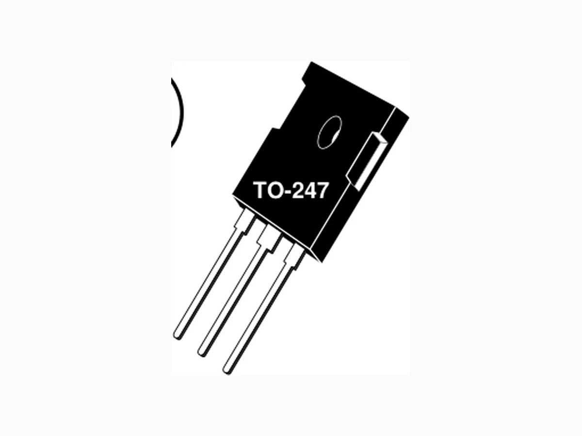
- Nitride Passivated Die for Improved Reliability. TO-247 ARF449A ARF449B G D S Common Source CAUTION: These Devices are Sensitive to Electrostatic Discharge. Proper Handling Procedures Should Be Followed. APT Website - http://www.advancedpower.com
DYNAMIC CHARACTERISTICS ARF449A/449B Symbol Ciss Coss Crss td(on) tr td(off) tf Characteristic Input Capacitance Output Capacitance Reverse Transfer Capacitance Turn-on Delay Time Rise Time Turn-off Delay Time Fall Time Test Conditions V GS = 0V VDS = 150V f = 1 MHz VGS = 15V VDD = 0.5 VDSS ID = ID[Cont.] @ 25°C RG = 1.6ý MIN TYP MAX 980 1200 87 120 25 40 51 0 3.1 7 15 25 UNIT pF ns FUNCTIONAL CHARACTERISTICS Symbol GPS η ψ Test Conditions f = 81.36 MHz VGS = 0V VDD = 150V Pout = 90W No Degradation in Output Power Characteristic Common Source Amplifier Power Gain Drain Efficiency Electrical Ruggedness VSWR 20:1 MIN TYP MAX 12 13 70 75 UNIT dB
1 Pulse Test: Pulse width < 380 µS, Duty Cycle < 2%
APT Reserves the right to change, without notice, the specifications and information contained herein. 1 5 10 50 100 500 GAIN (dB) FREQUENCY (MHz) Figure 1, Typical Gain vs Frequency 030 45 60 75 90 105 120 Class C VDD = 150V Pout = 150W 0 2 468 CAPACITANCE (pf) VDS, DRAIN-TO-SOURCE VOLTAGE (VOLTS) Figure 2, Typical Capacitance vs. Drain-to-Source Voltage 3000 1000 500 100 1 5 10 50 150 ID, DRAIN CURRENT (AMPERES) VDS, DRAIN-TO-SOURCE VOLTAGE (VOLTS) Figure 4, Typical Maximum Safe Operating Area VGS, GATE-TO-SOURCE VOLTAGE (VOLTS) Figure 3, Typical Transfer Characteristics ID, DRAIN CURRENT (AMPERES) VDS> ID (ON) x RDS (ON)MAX. 250µSEC. PULSE TEST @ <0.5 % DUTY CYCLE TJ = -55°C TJ = -55°CTJ = +125°C TJ = +25°C TC =+25°C TJ =+150°C SINGLE PULSE OPERATION HERE LIMITED BY RDS (ON) Ciss Coss Crss 10µS 1mS 10mS 100mS DC 100µS
C2-C4 -- Arco 463 Mica Trimmer C5-C7 -- 1nF 500V COG chip L1 -- 0.8" #18 AWG into hairpin ~19nH L2-L3 -- 3t #18 AWG .25" ID ~50nH L4 -- 10t #18 AWG .25" ID ~470nH L5 -- VK200-4B ferrite choke ~3uH R1 -- 25 Ohm 1/2W Carbon T1 -- 4:1 Broadband Transformer
81.36 MHz Test Circuit
15.49 (.610) 16.26 (.640) 5.38 (.212) 4.50 (.177) Max. 19.81 (.780) 20.32 (.800) 20.80 (.819) 21.46 (.845) 1.65 (.065) 2.13 (.084) 1.01 (.040) 1.40 (.055) 5.45 (.215) BSC 3.55 (.138) 3.81 (.150) 2.87 (.113) 3.12 (.123) 4.69 (.185) 5.31 (.209) 1.49 (.059) 2.49 (.098) 2.21 (.087) 2.59 (.102) 0.40 (.016) 0.79 (.031) Source 2-Plcs. Top View ARF449A Device ARF449B Gate Drain Source Source Drain Gate Dimensions in Millimeters and (Inches) NOTE: The ARF446 and ARF447 comprise a symmetric pair of RF power transistors and meet the same electrical specifications. The device pin-outs are the mirror image of each other to allow ease of use as a push-pull pair. ARF449A/449B APT’s products are covered by one or more of U.S.patents 4,895,810 5,045,903 5,089,434 5,182,234 5,019,522 5,262,336 6,503,786 5,256,583 4,748,103 5,283,202 5,231,474 5,434,095 5,528,058 and foreign patents. US and Foreign patents pending. All Rights Reserved.