
APM80900 ALLEGRO
Document overview
- Manufacturer or author: Provided By www.digicamel.com(free datasheet download site)
- PDF pages: 26
Technical content
DESCRIPTION
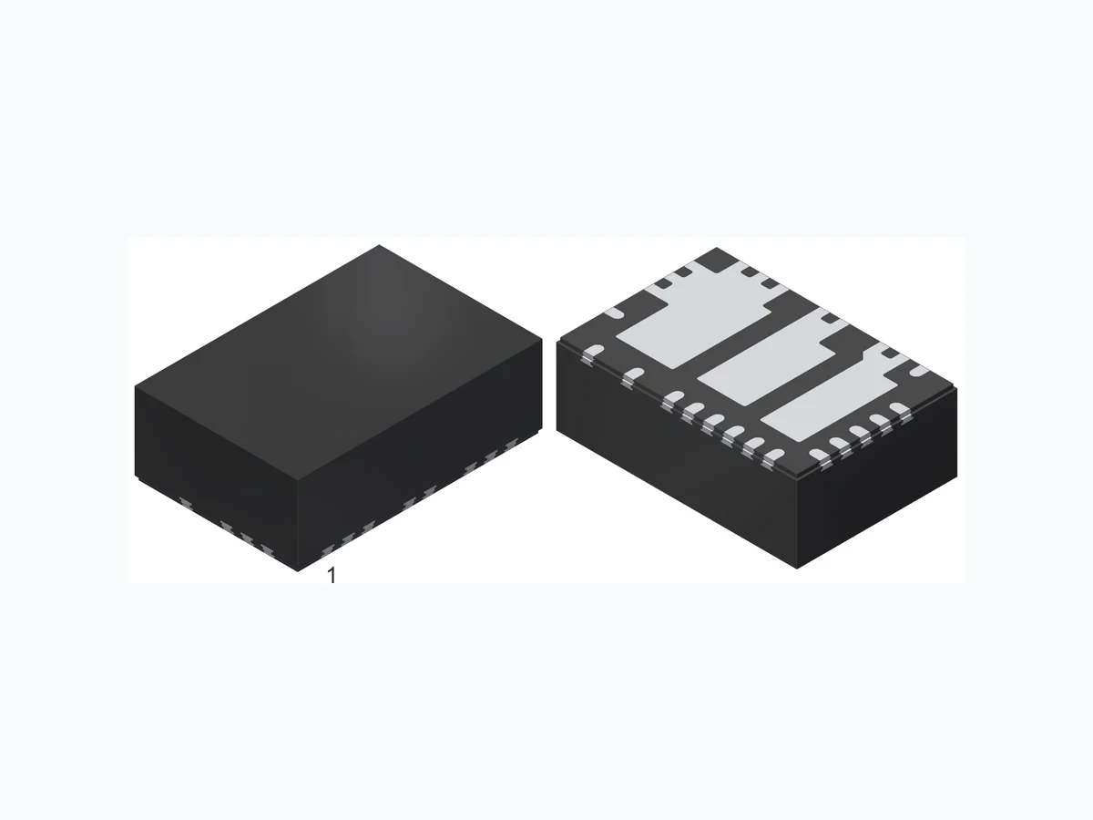
The APM80900 is a complete synchronous buck switching regulator module that provides constant current output to drive high-power LEDs. It integrates both high-side and low-side N-channel switches, inductor, high frequency VIN and boot capacitors. A true average current is output using a cycle-by- cycle, controlled on-time method. Output current is user-selectable by an external current sense resistor. Output voltage automatically adjusts to the LED string voltage to ensure optimal system efficiency. LED dimming is accomplished by a direct logic input pulse- width modulation (PWM) signal at the PWM pin while EN is enabled. Alternatively, applying a PWM signal at the EN pin while the PWM pin is high provides “chopped battery” PWM dimming for legacy control modules. The analog dimming input (ADIM pin) can be used to calibrate the LED current or implement thermal foldback in conjunction with an external NTC thermistor. The APM80900 is provided in a compact, thermally enhanced 4 mm × 6 mm × 2.1 mm QFN-32 package with wettable flanks. APM80900-DS, Rev. 2 MCO-0001053 FEATURES AND BENEFITS
- Automotive AEC-Q100 qualified
- Supply voltage 4.5 to 36 V , maximum 40 V
- Complete 1.5 A maximum output compact LED driver
- Integrated inductor, VIN, and boot capacitors
- Ultra-low EMI architecture, fSW > 2 MHz
- Spread spectrum for improved EMC
- Integrated high-side and low-side MOSFETs: 80 mΩ / 60 mΩTYP , 90% efficiency at 1 A
- 5 V , 14 mA LDO regulator for peripheral circuits
- Dimming via external PWM or EN pin
- Analog dimming for brightness calibration and thermal foldback
- Low power shutdown (1 μA typical)
- High side current sense, ±3% accuracy
- Fault flag output
- LED open fault mask setting for low VIN operation
- Undervoltage lockout (UVLO) and thermal shutdown protection
- Robust protection against: □ Adjacent pin-to-pin short □ Pin-to-ground short □ Component open/short faults Automotive-Grade, Low-EMI, 1.5 A PWM Dimmable Synchronous Buck LED Module PACKAGE: Not to scale APM80900 Figure 1: APM80900 Typical Application Circuit APPLICATIONS:
- Daytime running lights
- Front and rear fog lights
- Turn/stop lights
- Map light
- Dimmable interior lights
- Puddle lights 32-pin QFN 4 mm × 6 mm × 2.1 mm with wettable flank (suffix NB) November 29, 2022 VIN EN PWM ADIM RNG SGND PGND CSH CSL FFn FFn VOUT VCC FDSET APM80900 Ω Ω Ω
Automotive-Grade, Low-EMI, 1.5 A PWM Dimmable Synchronous Buck LED Module APM80900 Allegro MicroSystems
955 Perimeter Road
Manchester, NH 03103-3353 U.S.A. www.allegromicro.com SELECTION GUIDE Part Number Temperature Range Package Packing APM80900KNBATR –40°C to 150°C 32-pin 4 mm × 6 mm × 2.1 mm QFN with wettable flanks 3000 pieces per 13-inch reel ABSOLUTE MAXIMUM RATINGS Characteristic Symbol Notes Rating Unit Supply Voltage VVIN −0.3 to 40 V EN Voltage VEN –0.3 to VVIN + 0.3 V Current Sense Voltages VCSH, VCSL –0.3 to VVIN + 0.3 V VCC, ADIM, RNG, FDSET, FFn, and PWM Terminal Voltages VVCC, VADIM, VRNG, VFDSET, VFFn, VPWM –0.3 to 7 V Bootstrap Voltage VBOOT –0.3 to VVIN + 8 V Switching Voltage VSW Continuous –0.3 to VVIN + 0.3 V Pulsed, t < 50 ns –1 to VVIN + 3 V Maximum Junction Temperature TJ(max) 150 °C Storage Temperature Tstg –55 to 150 °C THERMAL CHARACTERISTICS* : May require derating at maximum conditions; see application section for optimization Characteristic Symbol Test Conditions* Value Unit Package Thermal Resistance (Junction to Ambient) RθJA On 4-layer PCB based on JEDEC standard 30 °C/W Package Thermal Resistance (Junction to Pad) RθJP 2 °C/W *Additional thermal information available on the Allegro™ website. SPECIFICATIONS Table of Contents Features and Benefits 1 Description 1 Applications 1 Package 1 Typical Application Circuit 1 Selection Guide 2 Absolute Maximum Ratings 2 Thermal Characteristics 2 Pinout Diagram and Terminal List 3 Functional Block Diagrams 4 Electrical Characteristics 5 EMC Performance Characteristics 7 Thermal Performance Characteristics 8 Functional Description 9 Application Circuit Diagrams 18 Package Outline Drawing 24
Automotive-Grade, Low-EMI, 1.5 A PWM Dimmable Synchronous Buck LED Module APM80900 Allegro MicroSystems Manchester, NH 03103-3353 U.S.A. www.allegromicro.com QFN-32 Pinout Diagram 31 30 28 12 13 14 15 16 VOUT VOUT VOUT VIN VIN PGND PGND EN FFn ADIM FDSET PWM SW BOOT CSH CSL SGND RNG VCC SW VOUT VOUT VOUT NC NC PAD1: VIN PAD0: PGND PAD2: VOUT Terminal List Number Name Function 1, 2, 3, 30, 31, 32 VOUT Output of converter. Sources LED current. 5, 6 VIN Input voltage supply for power stage. 8, 9 PGND Power ground terminal. 10 EN Enable pin for all IC functions. EN pin can also be used for PWM dimming when PWM pin is High.
12 PWM Logic input for PWM dimming: When PWM = Low, LED is OFF;
if PWM = High and EN = High, LED is ON.
13 FDSET
Sets LED Open fault mask threshold. Connect to a voltage divider formed between VIN and SGND. When VIN is low, resulting in FDSET below the internal reference, LED Open Fault detection will be masked. 14 ADIM Analog dimming control voltage input. 15 FFn Open-drain output that is pulled low when a fault occurs. Connect through an external pull-up resistor to the desired logic level. 16, 17 NC Recommend connecting to PGND 18 VCC Internal IC bias regulator output. Connect 1 µF MLCC to PGND. Can be used to supply up to 14 mA to an external load. 19 RNG Output current range select pin. Connect to VCC or GND to select high or low output current range. 20 SGND Signal ground terminal. 21 CSL Current Sense (negative end) feedback input for LED current. 22 CSH Current Sense (positive end) feedback input for LED current. 24 BOOT High-side gate driver bootstrap terminal (for test only). Leave this pin disconnected. 26, 28 SW Switch terminal (for test only). Leave this pin disconnected. PAD0 PAD Exposed pad for enhanced thermal dissipation; connect to PGND plane. PAD1 PAD Exposed pad for enhanced thermal dissipation; connect to VIN. PAD2 PAD Exposed pad for enhanced thermal dissipation; connect to VOUT. PINOUT DIAGRAM AND TERMINAL LIST
Automotive-Grade, Low-EMI, 1.5 A PWM Dimmable Synchronous Buck LED Module APM80900 Allegro MicroSystems Manchester, NH 03103-3353 U.S.A. www.allegromicro.com Figure 2: Functional Block Diagram PGND VVIN CIN PWM Cbias Rsense PGND VOUT BOOT PGND CSH CSL VIN PWM VCC CLED VIN On-Time select Buck Converter duty cycle control Vout Internal 5.0 V bias Vref (0 – 200 mV)i_LED referenceADIMADIM On-me VIN Fault FFn FAULT VCC LED current Gate driver Differenal Amp SGND Up to 14 mA external load VCSREG EN UVLO Other Faults 17 ms Boot Charger SW VIN LDO APM80900 RNG FDSET REF1 -+LED Open Fault LED Short Fault Vout VVIN 140 kΩ 100 kΩ 200 kΩ VCC
Automotive-Grade, Low-EMI, 1.5 A PWM Dimmable Synchronous Buck LED Module APM80900 Allegro MicroSystems Manchester, NH 03103-3353 U.S.A. www.allegromicro.com ELECTRICAL CHARACTERISTICS: Valid at VVIN = 12 V, VVOUT = 6 V, TJ = –40°C to 125°C, typical values at TJ = 25°C, unless otherwise noted Characteristics Symbol Test Conditions Min. Typ. Max. Unit Input Supply Voltage VVIN 4.5 – 36 V VVIN Undervoltage Lockout Threshold VUVLO(ON) VVIN increasing – – 4.31 V VVIN Undervoltage Lockout Hysteresis VUVLO(HYS) VVIN decreasing 100 – 300 mV VIN Pin Supply Current IVIN VCSH – VCSL = 0.5 V, VEN = VIH(EN), VPWM = VIH(PWM) – 5 – mA VIN Pin Shutdown Current [1] IVIN(SD) VEN = VIL(EN), TJ ≤ 85°C, VSW = 0 V – 1 10 µA Output Current Sense Common Mode Voltage (measured at CSL pin) [1] VVOUT VVIN = 36 V 2.65 – 25 V Buck Switch Current Limit Threshold ISW(LIM) 2.5 3.1 3.6 A Buck High-Side Switch On-Resistance RDSON(HS) VBOOT = VVIN + 4.3 V, TJ = 25°C, ISW = 0.5 A – 0.08 – Ω Buck Low-Side Switch On-Resistance RDSON(LS) VBOOT = 4.3 V, TJ = 25°C, ISW = 0.5 A – 0.06 – Ω Switching Minimum Off-Time tOFF(MIN) VCSH – VCSL = 0 V 50 65 80 ns Switching Minimum On-Time tON(MIN) 65 80 95 ns Selected On-Time tON VVIN = 12 V, VVOUT = 6 V – 250 – ns tON Spread Spectrum Range fSW(SWEEP) – ±5 – % Spread Spectrum Modulation Frequency fSW(MOD) – 11.5 – kHz REGULATION COMPARATOR AND ERROR AMPLIFIER Load Current Sense Regulation Threshold at 100% [2] VCSREG VCSH – VCSL decreasing, SW turns on, ADIM tied to VCC RNG = High 194 200 206 mV RNG = Low 96 100 104 mV CSH Input Sense Current [3] ICSH VCSH – VCSL = 0 V – 170 – µA CSL Input Sense Current ICSL VCSH – VCSL = 0 V – 170 – µA INTERNAL LINEAR REGULATOR VCC Regulated Output VVCC 0 mA < IVCC < 14 mA, VVIN > 6 V 4.85 5.0 5.15 V VCC Dropout Voltage VLDO Measure VVIN – VVCC: VVIN = 4.8 V, IVCC = 14 mA – 0.3 0.6 V VCC Current Limit iVCC(LIM) VVCC ≥ 4.35 V 20 – – mA VCC Undervoltage Lockout VVCC(UVLO) Rising 3.6 3.9 4.15 V VVCCUVLO(HYS) Hysteresis 180 230 280 mV EN INPUT Maximum IC Turn Off Delay tOFF(DELAY) Measured while PWM dimming signal applied at EN keeping low and exceeding tOFF(DELAY) results in shutdown 10 17 – ms Logic High Voltage VIH(EN) VEN increasing 1.8 – – V Logic Low Voltage VIL(EN) VEN decreasing – – 0.4 V EN Pull-Down Resistance REN(PD) – 140 – kΩ PWM INPUT Logic High Voltage VIH(PWM) VPWM increasing 1.8 – – V Logic Low Voltage VIL(PWM) VPWM decreasing – – 1.2 V PWM Pin Pull-Down Resistance RPWM(PD) – 100 – kΩ Continued on the next page…
Automotive-Grade, Low-EMI, 1.5 A PWM Dimmable Synchronous Buck LED Module APM80900 Allegro MicroSystems Manchester, NH 03103-3353 U.S.A. www.allegromicro.com Characteristics Symbol Test Conditions Min. Typ. Max. Unit RNG INPUT RNG Logic High VIH(RNG) VRNG increasing 1.8 – – V RNG Logic Low VIL(RNG) VRNG decreasing – – 0.8 V RNG Pull-Up Resistance to VCC RRNG(PU) – 200 – kΩ ANALOG DIMMING INPUT Input Voltage For >94% LED Current VADIM(H) VCSH – VCSL = VCSREG RNG = High 1.5 – – V Input Voltage For >90% LED Current VADIM(L) VCSH – VCSL = VCSREG RNG = Low 1.0 – – V Regulation Threshold at 50% Analog Dimming VCSREG(50) VADIM = 0.9 V RNG = High – 100 – mV VADIM = 0.65 V RNG = Low – 50 – mV Regulation Threshold at 20% Analog Dimming VCSREG(20) VADIM = 0.6 V RNG = High 38 40 42 mV FAULT ADIM Threshold for LED Open/Short Fault Detection VADIM(FAULT) VADIM rising 475 500 525 mV Output Voltage Low Threshold for LED Short Fault Detection VOUT(SHORT) VVOUT falling; VADIM = 5 V 1.3 1.5 1.7 V LED Open Fault Enable Reference VREF1 2.352 2.4 2.448 V LED Open Fault Current Threshold VCS(OPEN) VCSREG = 200 mV start falling (PWM duty = max), VADIM = VVCC, VFDSET = VVCC 35 65 95 mV LED Open Fault Current Hysteresis [1] VCS(OPENHYS) VCSREG = 200 mV start falling (PWM duty = max), VADIM = VVCC, VFDSET = VVCC 8 14 24 mV Fault Deglitch Timer tFDG 30 50 65 µs Fault Mask Timer tMASK 70 100 130 µs FFn Pull-Down Voltage VFAULT(PD) Fault condition asserted, pull-up current = 1 mA – – 0.4 V FFn Pin Leakage Current IFAULT(LKG) Fault condition cleared, pull-up to 5 V – – 1 µA FFn Rising Timer [1] tRISE Transition time Fault pin takes from Low to High – – 10 µs FFn Falling Timer [1] tFALL Transition time Fault pin takes from High to Low – – 10 µs Cool Down Timer for Fault Retry tRETRY – 1 – ms THERMAL SHUTDOWN Thermal Shutdown Threshold [1] TSD 150 165 180 °C Thermal Shutdown Hysteresis [1] TSD(HYS) – 25 – °C [1] Determined by design and characterization. Not production tested. [2] In test mode, a ramp signal is applied between CSH and CSL pins to determine the VCSH – VCSL regulation threshold voltage. In actual application, the average VCSH – VCSL voltage is regulated at VCSREG regardless of ripple voltage. [3] Negative current is defined as coming out of (sourcing) the specified device pin or node. ELECTRICAL CHARACTERISTICS (continued): Valid at VVIN = 12 V, VVOUT = 6 V, TJ = –40°C to 125°C, typical values at TJ = 25°C, unless otherwise noted
Automotive-Grade, Low-EMI, 1.5 A PWM Dimmable Synchronous Buck LED Module APM80900 Allegro MicroSystems Manchester, NH 03103-3353 U.S.A. www.allegromicro.com EMC PERFORMANCE CHARACTERISTICS VVIN = 12 V, TA = 25°C, Load = 2 series white LEDs, ILED = 0.5 A, with EMI filters, as shown in Figure 3 EN55025/CISPR25 Class 5 Peak and Average Conducted Emissions (150 kHz to 108 MHz) EN55025/CISPR25 Class 5 Peak and Average Rod Antenna Radiated Emissions (150 kHz to 30 MHz) EN55025/CISPR25 Class 5 Peak and Average Biconical Radiated Emissions (Horizontal, 30 MHz to 330 MHz) EN55025/CISPR25 Class 5 Peak and Average Biconical Radiated Emissions (Vertical, 30 MHz to 330 MHz)
Automotive-Grade, Low-EMI, 1.5 A PWM Dimmable Synchronous Buck LED Module APM80900 Allegro MicroSystems Manchester, NH 03103-3353 U.S.A. www.allegromicro.com Figure 3: EMC test circuit 0.047 µF 4.7 µF 1 µF APM80900 10 kΩ 100 kΩ VOUTVIN PGND FFn ADIM PWM FDSET EN CSH CSL SGND RNG VCC VVIN VCC Fault 0.2 Ω 374 kΩ For best performance, locate C2 close to CSL pin with a low impedance path to PGND of the IC. THERMAL PERFORMANCE CHARACTERISTICS VVIN = 12 V, 2 WLEDs / 1 A, Ƞ = 89% VVIN = 24 V, 2 WLEDs / 1 A, Ƞ = 82%
Automotive-Grade, Low-EMI, 1.5 A PWM Dimmable Synchronous Buck LED Module APM80900 Allegro MicroSystems Manchester, NH 03103-3353 U.S.A. www.allegromicro.com The APM80900 is a complete low-EMI synchronous buck regu- lator module designed for driving a high-current LED string. The operational VVIN range is from 4.5 to 36 V , and it can withstand up to 40 V input transients. This module can regulate LED cur- rent from 200 mA to 1.5 A, depending on thermal management. It uses average current mode control to maintain constant LED current for consistent brightness. The LED current level is easily programmable by selection of an external sense resistor, with a value determined as follows: RSENSE = VCSREG / iLED There are two options of VCSREG for high or low output current range. If output LED current is between 0.6 and 1.5 A, the RNG pin should be connected to logic high signal (VCC) or left open. If output LED current is between 200 and 600 mA, the RNG pin should be connected to GND for reduced power dissipation. Table 1: RNG setting for suggested LED Output Current Range RNG VCSREG ILED High 200 mV (typical) 0.6 to 1.5 A Low 100 mV (typical) 200 to 600 mA Synchronous Regulation The APM80900 integrates an N-channel DMOS as the low-side and high-side switches to implement synchronous regulation for LED drivers, as shown in Figure 4. CBOOT BOOT GND VIN Floating gate driver Integrated switch SW L i_L RSENSE CLED Boot Charger VOUT SW APM80900 Figure 4: Synchronous Buck LED Driver The synchronous configuration can effectively pull SW to GND by forcing the low-side synchronous switch on even with small inductor current. Therefore, the internal boot capacitor can be charged normally every switch cycle to ensure the normal opera- tion of the buck LED driver. An extremely low switch deadtime ensures that minimal power is dissipated during the high-side switch turn-on transition. This low deadtime also reduces EMI. The integrated VIN to PGND capacitor significantly reduces the high-current input loop length, greatly reducing the radiated emissions. Switching Frequency The APM80900 operates in fixed on-time mode during switching. The on-time (and hence switching frequency) is programmed by an internal circuit to keep switching frequency at around 2 MHz across the operating range. Note that tON must be greater than tON(MIN), which is 80 ns (typical). If VVIN is high enough to reach tON(MIN), the APM80900 will maintain tON(MIN) even when VVIN increases further. tON = max[tON(MIN) , 1 / (2 MHz) × (VVOUT / VVIN)] The switching frequency of the converter may vary with output current due to voltage drop on the switches and inductor when conducting. To minimize the peaks of switching frequency harmonics in EMC measurement, a spread spectrum feature is implemented. The spread spectrum range is internally set at ±5%. The actual switch- ing frequency is swept linearly between 0.95 × fSW and 1.05 × fSW, where fSW is the programmed switching frequency. The rate of modulation for fSW is fixed internally at 11.5 kHz. Enable and Dimming The APM80900 is activated when a logic-high signal is applied to the EN (enable) pin and VVIN is above UVLO threshold, 4.31 V . The buck converter ramps up the LED current to a target level set by RSENSE when PWM pin = High. The EN pin is high-voltage tolerant and can be directly con- nected to a power supply. However, if VEN is higher than VVIN at any time, a series resistor (10 kΩ) is required to limit the current flowing into the EN pin. This resistor is helpful in preventing EN from damage in case of reverse battery connection. This series resistor is not necessary if EN is driven from a logic input. The PWM pin is a logic input pin and is internally pulled down through a resistor. If the APM80900 is enabled before the PWM sig- nal is asserted high, the output remains off until PWM signals start. FUNCTIONAL DESCRIPTION
Automotive-Grade, Low-EMI, 1.5 A PWM Dimmable Synchronous Buck LED Module APM80900 Allegro MicroSystems Manchester, NH 03103-3353 U.S.A. www.allegromicro.com The EN and PWM pins function as shown in Table 2. Table 2: EN and PWM Pin Function EN pin PWM pin VCC LED High Low/Open ON OFF High High ON ON Low (<tOFF(DELAY)) x ON OFF Low (>tOFF(DELAY)) x Shutdown When the EN pin is forced from high to low, the LED current is turned off, but the IC remains in standby mode for up to at least 10 ms. If EN goes high again within this period, the LED current is turned on immediately if PWM pin is high. If EN pin is low for more than tOFF(DELAY), the IC enters shutdown mode to reduce power consumption. The next high signal on EN will initialize a full startup sequence, which includes a startup delay of approxi- mately 150 μs. This startup delay is not present during PWM operation. Active dimming of the LED is achieved with 2 options: by sending a PWM (pulse-width modulation) signal to the EN pin (while PWM = High); or by sending a dimming PWM signal to the PWM pin while EN = High. The resulting LED brightness is proportional to the duty cycle of the applied PWM signal. A practical range for PWM dimming frequency is between 100 Hz (period 10 ms) and 2 kHz. If the PWM dimming signal at the PWM pin is low when the EN pin is high, the LED will be off immediately, and the IC remains enabled, waiting for the next PWM pulse. The internal LDO is still on and can provide bias to the internal and external circuits. PWM Dimming Ratio The brightness of the LED string can be changed by adjusting the PWM duty cycle as follows: Dimming ratio = PWM on-time / PWM period For example, by selecting a PWM period of 5 ms (200 Hz PWM frequency) and a PWM on-time of 5 µs, a dimming ratio of 0.1% can be achieved. This is sometimes referred to as “1000:1 dim- ming.” In an actual application, the minimum dimming ratio is deter- mined by various system parameters, including: VVIN , VVOUT , inductance, LED current, and PWM frequency. The device is easily capable of PWM on-time as short as 5 µs; however, if fault flag for open/short LED detection is required, it should be above 130 µs due to the fault mask timer. Analog Dimming In addition to PWM dimming, the APM80900 also provides an analog dimming feature. If RNG = High, when VADIM is over 1.5 V , the LED current is at 100% level (as defined by the sense resistor RSENSE). When VADIM is between 0.6 and 1.3 V , the LED current changes linearly with VADIM from 20% to 90%. Within this range, the LED current reference voltage VCS can be calculated as: VCSREG = (VADIM – 0.4 V) ⁄ 5 This is shown in Figure 5. RNG = High 1.3 V 200 mV (100%) 0.6 V 40 mV (20%) 100 mV (50%) 0.9 V0.4 V 180 mV (90%)
1.5 V VADIM
Figure 5: ADIM Pin Voltage controls the LED Current Reference Voltage with RNG = High If RNG = Low, when VADIM is over 1.0 V , the LED current is at 100% level (as defined by the sense resistor RSENSE). When VADIM is between 0.6 to 0.85 V , the LED current changes linearly with VADIM from 40% to 90%. Within this range, LED current reference voltage VCS can be calculated as: VCSREG = (VADIM – 0.4 V) ⁄ 5 This is shown in Figure 6. RNG = Low 0.85 V 100 mV (100%) 0.6 V 40 mV (40%) 50 mV (50%) 0.65 V0.4 V 90 mV (90%)
1.0 V VADIM
Figure 6: ADIM Pin Voltage controls the LED Current Reference Voltage with RNG = Low
Automotive-Grade, Low-EMI, 1.5 A PWM Dimmable Synchronous Buck LED Module APM80900 Allegro MicroSystems Manchester, NH 03103-3353 U.S.A. www.allegromicro.com For accurate LED current level control, the APM80900 should operate with ADIM in the linear region of 0.6 to 1.3 V for RNG = High and 0.6 to 0.85 V for RNG = Low. Note that the allowable voltage across the sensing resistor RSENSE should lie within the range of –50 to 250 mV to avoid saturating the internal current amplifiers. The expected minimum and maxi- mum vCS can be estimated by the following equations: min _ = [ − ( − ) 19.6 × ] × max _ = [ + ( − ) 19.6 × ] × where ILED is the expected LED output current. In order to extend the operation beyond VCS limits, an external inductor of 4.7 µH can be added to ensure proper operation with 5 or 6 WLEDs with VIN up to 36 V , as shown in Figure 7: VOUT CSH CSL 5 or 6 WLEDs LED+ GND Figure 7: An external inductor is added for 5 or 6 WLEDs operation with VIN up to 36 V The ADIM pin can be used in conjunction with PWM dimming to provide wider LED dimming range over 1000:1. In addition, the IC can provide thermal foldback protection by using an external NTC (negative temperature coefficient) thermistor, as shown in Figure 8. NTC Rp Rs VCC ADIM Figure 8: Using an External NTC Thermistor to Implement Thermal Foldback Based on the equation below, ADIM voltage will be reduced to lower the LED current for less LED power when temperature rise due to LED heating causes the resistance reduction of NTC thermistor. VADIM = VVCC × ([(RNTC (T) + Rs) // Rp]) / ([(RNTC (T) + Rs) // Rp + R1]) Minimum and Maximum Output Voltages With a typical minimum tOFF of 100 ns, the maximum duty cycle is approximately 80%. So for VVIN = 18 V , the maximum output is approximately 14.4 V (based on the simplified equation of VVOUT = VVIN × D). With a typical minimum tON of 80 ns, the minimum duty cycle is approximately 16%. That means with VVIN = 18 V , the theoreti- cal minimum VVOUT is just 1.8 V . However, the internal current sense amplifier is only designed to operate down to VVOUT = 2.65 V . Operating with VVOUT < 2.65 V will result in reduced current sense accuracy. If the required output voltage is lower than that permitted by the minimum tON, the controller will automatically extend the tOFF, in order to maintain the correct duty cycle. The result is that the switching frequency is reduced, in order to keep the LED current in regulation. If the LED string is completely shorted (VVOUT < 1.5V typical), the controller will continue to switch at minimum tON and will not enter Hiccup mode. Thermal Budgeting The APM80900 can supply a 1.5 A current to the LED string. However, depending on the duty cycle, the conduction loss in the high-side and low-side switches, and loss in the inductor may cause the package to reach the thermal shutdown threshold. Therefore, care must be taken to ensure the total power loss of the APM80900 is within budget. For example, if the maximum temperature rise allowed is ∆T = 60°C at the device case surface, then the maximum power dissipation of the module is 2 W when mounted to Allegro’s 4-layer PCB which has an RθJA of 30°C/W. When considering the switching and conduction losses within the APM80900, the esti- mated maximum LED current is limited to 1.5 A. Fault Handling The APM80900 is designed to handle the following faults.
- Pin-to-ground short
- Pin-to-neighboring pin short
- Pin open
- Opens/shorts on some external components
- Output short to ground
Automotive-Grade, Low-EMI, 1.5 A PWM Dimmable Synchronous Buck LED Module APM80900 Allegro MicroSystems Manchester, NH 03103-3353 U.S.A. www.allegromicro.com RSENSE Shorted Fault RSENSE short detection detects shorts across the RSENSE resis- tor, but is limited to hard shorts (very low impedance). A weak short will effectively reduce the value of the RSENSE resistance, resulting in greater output current. If the inductor current limit is not reached, this will not register as a short, a fault will not be asserted, and the IC will continue to regulate at higher than programmed LED current. LED Open/Output Short Faults The A80900 can detect an open LED string or output short fault and assert the fault flag by pulling the FFn pin low. The LED open fault is detected by monitoring the voltage, VCSREG, across the current sense resistor while the PWM signal is high, and LED short is detected when VOUT < 1.5 V while VADIM > 500 mV . The fault must remain present for more than the fault deglitch time, tFDG for the A80900 to act on fault condition. A fault mask timer, tMASK, starts at the rising edge of each PWM cycle to mask faults when the PWM cycle starts. If the PWM on-time is less than the fault mask timer, the fault flag will not assert. The fault flag state is latched when PWM goes low to maintain its high or low state until the next PWM rising edge. If an open LED fault is detected, the regulator will enter hiccup mode and assert the fault flag. If the open LED fault condition is removed, the fault flag is released after the next PWM rising edge and completion of either the hiccup timer or current to regulation timer; see cases 5, 6, and 7 in the LED Open/Short fault tim- ing diagrams. The open LED fault is masked and will not assert the fault flag if either of two conditions is met: VFDSET is below VREF1 or VADIM is below 500 mV . If the fault flag was asserted prior to either of these conditions, the fault flag will remain asserted. If the fault is removed while VFDSET is below VREF1 or VADIM is below 500 mV , the fault flag will be released. When an output short fault occurs, such as LED shorted to ground or output capacitor shorted to ground, the regulator will not enter hiccup mode and will continue to switch. When the short is removed, the APM80900 will return to normal operation.
Automotive-Grade, Low-EMI, 1.5 A PWM Dimmable Synchronous Buck LED Module APM80900 Allegro MicroSystems Manchester, NH 03103-3353 U.S.A. www.allegromicro.com 1 ms Hiccup Mode FFn FFn VCC FDSET SGND LED Open LED Short VIN REF1 SW Duty MaxDuty RSENSE Short, Inductor Open/Short, Overcurrent 1.5 V -VOUT 25% iLED -VCSREG ADIM 0.5 V Figure 9: LED Open/Short Fault Block Diagram FDSET PWM VCSREG REF1 25% × iLED FFn Flag LED OPEN FAULT LED OPEN FAULT (VADIM ≥ 0.5 V) Figure 10: LED Open/Short Fault Timing Diagram Table 3: LED Open Fault Truth Table FFn (N) FDSET ADIM LED Connection PWM FFn (N+1) Note Previous LED open fault state does not matter X High High Closed Circuit Next Rising Edge 1 Fault Flag does not assert (LEDs connected) X High High Open Circuit Next Rising Edge 0 Fault Flag asserts on next PWM edge Previous LED open fault state high (not asserted)
1 Low X X X 1
Fault flag does not assert when FDSET or ADIM are low
1 X Low X X 1
Previous LED open fault state low (asserted)
0 Low X Open Circuit X 0 Fault flag remains asserted if FDSET or ADIM go low
after fault occurred0 X Low Open Circuit X 0
0 Low X Closed Circuit Next Rising Edge 1 Fault flag de-asserts if LEDs reconnect even when
FDSET or ADIM is low0 X Low* Closed Circuit Next Rising Edge 1 ADIM low is < 500 mV. FDSET low is when FDSET < VREF1 (typical 2.4 V). * must be > 400 mV for FF to go high.
Automotive-Grade, Low-EMI, 1.5 A PWM Dimmable Synchronous Buck LED Module APM80900 Allegro MicroSystems Manchester, NH 03103-3353 U.S.A. www.allegromicro.com The Fault deglitch time tFDG, is fixed and is typically 50 µs. The Fault mask time, tMASK, is also fixed and is typically 100 µs (refer to Electrical Characteristics table). The Fault timing dia- gram is illustrated in Figure 11: tMASK Short Fault Short Removed Short Fault Short Removed Short Fault tFDG tMASK PWM FFn Figure 11a: LED Short Fault Timing Diagram Overview tMASK Open Fault Open Removed Open Fault Open Removed Open Fault tFDG tMASK PWM FFn SW ~1 ms Hiccup period ~1 ms Hiccup Current to regulation timer ~1 ms Hiccup ~1 ms Hiccup Current to regulation timer Figure 11b: LED Open Fault Timing Diagram Overview
Automotive-Grade, Low-EMI, 1.5 A PWM Dimmable Synchronous Buck LED Module APM80900 Allegro MicroSystems Manchester, NH 03103-3353 U.S.A. www.allegromicro.com The basic timing configurations are detailed below for LED Open/Short faults: Case 1: LED Open/Short Event is outside Mask Timer at PWM = H Case 2: LED Open/Short Event is within Mask Timer at PWM = H Mask Timer Fault Event Deglitch Timer PWM Fault Event Fault Flag LED Open/Short No LED Fault Mask Timer Fault Event Mask Timer PWM Fault Event Fault Flag LED Open/Short Case 3: LED Open/Short Event is close to PWM ↓ at PWM = H Case 4: LED Open/Short Event is at PWM = L Mask Timer Fault Event PWM Fault Flag Mask Timer Fault Event LED Open/Short Mask Timer No LED Fault Mask Timer Fault Event PWM Fault Flag Fault Event Mask Timer LED Open/Short Case 5: LED Open/Short Removed at PWM = L a) LED Short Removed at PWM = L b) LED Open Removed at PWM = L Mask Timer Fault Removed PWM Fault Flag Short Event Mask Timer No LED Short Mask Timer Fault Removed Fault Flag Open Event Current to regulation timer: * PWM No LED Open Case 6: LED Open/Short Removed outside Mask Timer at PWM = H a) LED Short Removed outside Mask Timer at PWM = H b) LED Open Removed outside Mask Timer at PWM = H Mask Timer Fault Removed PWM Fault Flag Short Event No LED Short LED Short Mask Timer Fault Removed Current to regulation timer * PWM Fault Flag Open Event LED Open Hiccup period: ~1 ms No LED Open Case 7: LED Open/Short Removed within Mask Timer at PWM = H a) LED Short Removed within Mask Timer at PWM = H b) LED Open Removed within Mask Timer at PWM=H Mask Timer Fault Removed PWM Fault Flag Short Event No LED Short LED Short Mask Timer Fault Removed Current to regulation Timer * PWM Fault Flag Open Event LED Open No LED Open * Current to regulation timer is 256 switching cycles.
Automotive-Grade, Low-EMI, 1.5 A PWM Dimmable Synchronous Buck LED Module APM80900 Allegro MicroSystems Manchester, NH 03103-3353 U.S.A. www.allegromicro.com SYSTEM FAILURE DETECTION AND PROTECTION DEMONSTRATION IC-Level Failure Modes Protected against - Any pin open - Any pin shorted to ground - Adjacent pin-to-pin short C5 = open or short RSENSE short C3 short LED string open or short to GND C1,C2 = open or short System-Level Failure Modes Protected against open/short fault for external components, including: - LED string - Sense resistor - Input/output caps, etc. VVIN EN GND OUT CSH CSL VIN EN PWM VCC APM80900 PWM C1 C2 RSENSE SGND PGND GND Figure 12: Demonstration of various possible fault cases in an application circuit Table 4: System Failure Mode Table (partial) Failure Mode Symptom Observed FAULT flag asserted? APM80900 Response Sense resistor shorted Dim light from LED Yes Triggers SW OCP fault, entering into Hiccup mode with about 1 ms retry period. LED string open [1] No light from LED Yes [1] Enter Hiccup mode with about 1 ms retry period. LED String shorted [2] (Either LED shorted to GND or Output capacitor shorted to GND). VOUT < 1.5 V. Dim or no light from LED Yes Continues switching at minimum tON; regulator will not enter Hiccup mode. [1] For LED Open Fault, fault flag will not be asserted when V VIN is below preset mask threshold, VADIM is below 500 mV or PWM dimming pulse width is below fault mask timer. [2] For LED Short Fault, fault flag will not be asserted when VADIM is below 500 mV or PWM dimming pulse width is below fault mask timer.
Automotive-Grade, Low-EMI, 1.5 A PWM Dimmable Synchronous Buck LED Module APM80900 Allegro MicroSystems Manchester, NH 03103-3353 U.S.A. www.allegromicro.com Output Filter Capacitor The APM80900 is designed to operate in current regulation mode. Therefore, it does not require a large output capacitor to stabilize the output voltage. This results in lower cost and smaller PCB area. In fact, having a large output capacitor is not recom- mended. In most applications, however, it is beneficial to add a small filter capacitor (approximately 0.047 μF) very close to the CSL pin of the IC with a good connection to PGND. This capacitor serves as a filter to eliminate switching spikes seen by the LED string. This is very important in reducing EMI noises, and may also help in ESD testing. Without output capacitor: The same inductor ripple current flows through sense resistor and LED string. iripple With a small capacitor across LED string: Ripple current through LED string is reduced, while ripple voltage across Rsense remains high. VVIN RSENSE GND VOUT iripple VVIN RSENSE GND VOUT iripple Figure 13: Using an Output Filter Capacitor to Reduce Ripple Current in LED String Effects of Output Capacitor on LED Ripple Current
Automotive-Grade, Low-EMI, 1.5 A PWM Dimmable Synchronous Buck LED Module APM80900 Allegro MicroSystems Manchester, NH 03103-3353 U.S.A. www.allegromicro.com APPLICATION CIRCUIT DIAGRAMS Figure 14: Application circuit example for APM80900 with 1 A LED current. 0.047 µF 4.7 µF 1 µF APM80900 10 kΩ 100 kΩ 374 kΩ VOUTVIN PGND FFn ADIM FDSET PWM EN CSH CSL SGND RNG VCC VVIN VCC Fault 0.2 Ω 8 to 36 V (1~6 LEDs) RSENSE For best performance, locate C2 close to CSL pin with a low imped- ance path to PGND of the IC. C1 Ceramic capacitor, 4.7 µF, 50 V, 10%, X7S, 0805 C2 Ceramic capacitor, 0.047 µF, 50 V, 10%, X7R, 0805 C3 Ceramic capacitor, 1 µF, 16 V, 10%, X7R, 0603 RSENSE Resistor, 0.2 Ω, 1/2 W, 1%, 1206 Fault Mask Threshold ≤ 2.4 ×(1 + 374 Ω 100 Ω)= 11.4
Automotive-Grade, Low-EMI, 1.5 A PWM Dimmable Synchronous Buck LED Module APM80900 Allegro MicroSystems Manchester, NH 03103-3353 U.S.A. www.allegromicro.com Efficiency vs. 2 WLEDs load 10% PWM Dimming Waveform at VVIN = 12 V 2 ms/div LED Current: 500 mA/div PWM: 2 V/div LED Voltage:
2 V/div
Input Startup Waveforms @ 2 WLEDs 1 ms/div
12 V - 20 V VIN Transient @ 2 WLEDs
PWM Startup Waveforms @ 2 WLEDs, VVIN = 12 V 2 µs/div PWM Shutdown Waveforms @ 2 WLEDs, VVIN = 12 V 2 µs/div VVIN: 5 V /div LED Current: 500 mA/div PWM: 2 V/div LED Voltage: LED Current: 500 mA/div PWM: 2 V/div LED Voltage: LED Current: 500 mA/div VVIN: 5 V/div LED Current: 200 mA/div
Automotive-Grade, Low-EMI, 1.5 A PWM Dimmable Synchronous Buck LED Module APM80900 Allegro MicroSystems Manchester, NH 03103-3353 U.S.A. www.allegromicro.com APPLICATION CIRCUIT DIAGRAMS (continued) Figure 15: Application circuit example with VVIN = 24 V ±10%, 4 WLEDs @ 1 A C1 Ceramic capacitor, 4.7 µF, 50 V, 10%, X7S, 0805 C2 Ceramic capacitor, 0.047 µF, 50 V, 10%, X7R, 0805 C3 Ceramic capacitor, 1 µF, 16 V, 10%, X7R, 0603 RSENSE Resistor, 0.2 Ω, 1/2 W, 1%, 1206 0.047 µF 4.7 µF 1 µF APM80900 10 kΩ 100 kΩ 374 kΩ VOUTVIN PGND FFn ADIM FDSET PWM EN CSH CSL SGND RNG VCC VVIN VCC Fault 0.2 Ω 1%24 V ±10%
4 WLEDs
For best performance, locate C2 close to CSL pin with a low imped- ance path to PGND of the IC.
24 V Input Startup Waveforms @ 4 WLEDs
24 V Input 10% PWM Dimming Waveform
LED Current: 500 mA/div PWM: 2 V/div LED Voltage:
5 V/div
VVIN: 5 V /div LED Current: 500 mA/div LED Voltage:
10 V /div
Automotive-Grade, Low-EMI, 1.5 A PWM Dimmable Synchronous Buck LED Module APM80900 Allegro MicroSystems Manchester, NH 03103-3353 U.S.A. www.allegromicro.com APPLICATION CIRCUIT DIAGRAMS (continued) Figure 16: Using 2 (or more) APM80900s in parallel to drive the same LED string. Total LED current is the sum of currents from each LED driver. (Note: Each LED driver shares the same VIN and ADIM as illustrated.) CBOOT BOOT GND VIN Floating gate driver Integrated switch L RSENSE1 CLED1 VVOUT Boot Charger OUT SW APM80900 ADIM FFn CBOOT BOOT GND VIN Floating gate driver Integrated switch L RSENSE2 CLED2 Boot Charger OUT SW APM80900 ADIM FFn Input Voltage ADIM Voltage5 V CSH1 CSL1 CSH2 CSL2 0.13 Ω 1% 20 kΩ 0.13 Ω 1% 3 A 0.1 µF 0.1 µF For best performance, locate CLED1 and CLED2 close to CSL pins with a low impedance path to PGND of the IC.
Automotive-Grade, Low-EMI, 1.5 A PWM Dimmable Synchronous Buck LED Module APM80900 Allegro MicroSystems Manchester, NH 03103-3353 U.S.A. www.allegromicro.com Figure 17: “One Out All Out” functionality can be implemented with 2 APM80900s driving different LED strings: When one module fails (e.g. due to LED short or open), its FFn drives other module’s ADIM Low and forces to turn OFF LED current. VIN EN PWM ADIM VCC SGND PGND CSH CSL FFn FFn1 LED+ GND VOUT APM80900 VIN EN PWM ADIM VCC SGND PGND CSH CSL FFn FFn2 LED+ GND VOUT APM80900 ADM1 ADM2 LED1 LED2 For best performance, locate CLED1 and CLED2 close to CSL pins with a low impedance path to PGND of the IC. CLED1 CLED2 APPLICATION CIRCUIT DIAGRAMS (continued)
Automotive-Grade, Low-EMI, 1.5 A PWM Dimmable Synchronous Buck LED Module APM80900 Allegro MicroSystems Manchester, NH 03103-3353 U.S.A. www.allegromicro.com APPLICATION CIRCUIT DIAGRAMS (continued) Figure 18: Application circuit example at VVIN = 30 V ±10% to drive 3 red LEDs @ 1.5 A with external PWM dimming at 30 Hz, 3% duty cycle. 0.047 µF 4.7 µF 1 µF APM80900 10 kΩ 100 kΩ 374 kΩ VOUTVIN PGND FFn ADIM FDSET PWM EN CSH CSL SGND RNG VCC VVIN VCC Fault 0.13 Ω 1%30 V ±10%
3 Red LEDs
PWM = 30 Hz, 3% duty cycle RSENSE 10 kΩ For best performance, locate C2 close to CSL pin with a low impedance path to PGND of the IC. C1 Ceramic capacitor, 4.7 µF, 50 V, 10%, X7S, 0805 C2 Ceramic capacitor, 0.047 µF, 50 V, 10%, X7R, 0805 C3 Ceramic capacitor, 1 µF, 16 V, 10%, X7R, 0603 RSENSE Resistor, 0.13 Ω, 1/2 W, 1%, 1206
30 V Input, 30 Hz 3% PWM Dimming Waveform
2 µs/div LED Current: 500 mA/div PWM: 2 V/div LED Voltage:
5 V/div LED Voltage:
LED Current: 500 mA/div PWM: 2 V/div
Automotive-Grade, Low-EMI, 1.5 A PWM Dimmable Synchronous Buck LED Module APM80900 Allegro MicroSystems Manchester, NH 03103-3353 U.S.A. www.allegromicro.com Figure 19: 32-pin 4 mm × 6 mm × 2.1 mm QFN with wettable flank (suffix NB) A 6.00 ±0.15 4.00 ±0.15 A Terminal #1 mark area PRELIMINARY For Reference Only; Not for Tooling Use (Reference DWG-0000753, Rev. 1) Dimensions in millimeters Exact case and lead configuration at supplier discretion within limits shown C Branding scale and appearance at supplier discretion B Coplanarity includes exposed thermal pad and terminals C Standard Branding Reference View 1 Line 1: Part Number Line 2: Logo A, 4-Digit Date Code Line 3: Characters 5, 6, 7, 8 of Assembly Lot Number Center aligned Pin 1 dot top left XXXXXX Lot Number Date Code 1213141516 0.25 ±0.05 0.50 R0.125 0.40 ±0.10 28 30 31 32 DETAIL A
0.30 MIN
0.00–0.05 0.08 C 32× B 2.10 ±0.10 SEATING PLANE PLATED AREA
0.05 SET BACK
3× 0.45 1.225 ±0.10 1.45 ±0.10 1.00 ±0.10 2.50 ±0.10 0.75 45° 0.655 0.85 6× 0.30 MIN 6× 0.35 0.625 0.625 0.75 6× 0.30 2.30 ±0.10 2.50 ±0.10 0.10 C2× 0.10 C2× PACKAGE OUTLINE DRAWING
Automotive-Grade, Low-EMI, 1.5 A PWM Dimmable Synchronous Buck LED Module APM80900 Allegro MicroSystems Manchester, NH 03103-3353 U.S.A. www.allegromicro.com PCB Footprint – Copper PCB Footprint – Paste PCB Footprint – Soldermask 4.80 0.30 ×4 1.45 0.25 2.50 2.30 1.25 0.45 0.40 2.50 2.80
0.50 TYP
0.30 ×25 0.85 ×15 6.80 45° R0.05 0.30 ×2 0.75 1.00 2.85 2.95 4.80 0.75 ×3 2.00 2.25 1.35 0.95 1.00 0.70 0.75 1.80 2.15 2.00 2.25 0.70 0.30 ×25 0.85 ×25 6.80 R0.05 1.20 0.851.25 2.853.20 0.05 MAX0.50 TYP METAL SOLDERMASK OPENING Figure 20: Recommended PCB Footprint Altium and Cadence schematic and layout library files for the APM80900 are provided on the APM80900 product page on Allegromicro.com.
Automotive-Grade, Low-EMI, 1.5 A PWM Dimmable Synchronous Buck LED Module APM80900 Allegro MicroSystems Manchester, NH 03103-3353 U.S.A. www.allegromicro.com For the latest version of this document, visit our website: www.allegromicro.com
Revision History
– March 30, 2021 Initial release
1 July 26, 2022 Updated Figure 3; removed Solder Reflow Considerations section
2 November 29, 2022 Added PCB footprint (page 25)
Copyright 2022, Allegro MicroSystems. Allegro MicroSystems reserves the right to make, from time to time, such departures from the detail specifications as may be required to permit improvements in the performance, reliability, or manufacturability of its products. Before placing an order, the user is cautioned to verify that the information being relied upon is current. Allegro’s products are not to be used in any devices or systems, including but not limited to life support devices or systems, in which a failure of Allegro’s product can reasonably be expected to cause bodily harm. The information included herein is believed to be accurate and reliable. However, Allegro MicroSystems assumes no responsibility for its use; nor for any infringement of patents or other rights of third parties which may result from its use. Copies of this document are considered uncontrolled documents.