

 Download PDF
APD-SERIES SKYWORKS
Document overview
- PDF pages: 8
Technical content
Page 1
DATA SHEET
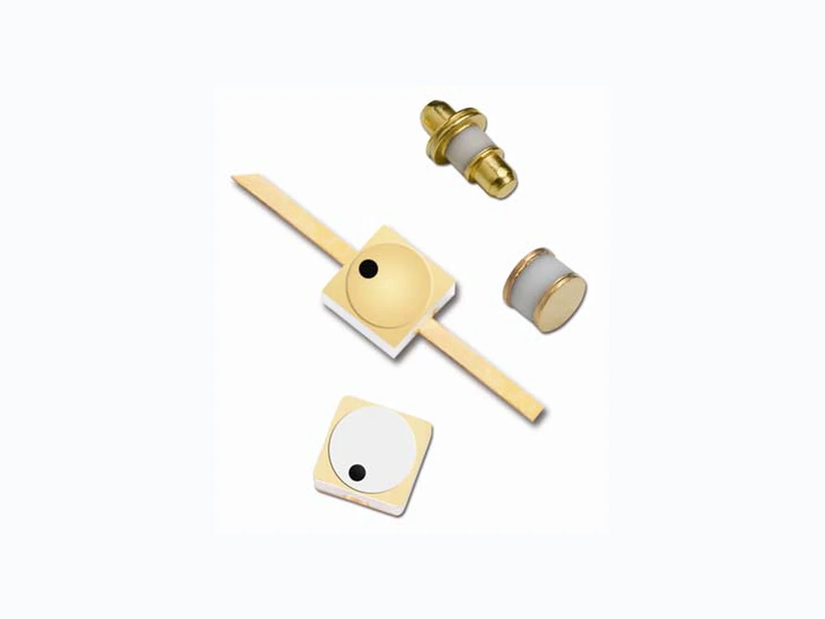
APD Series: Hermetic Ceramic Packaged Silicon PIN Diode
Devices
Applications
Switches Attenuators
Features
Established PIN diode process Low capacitance designs Voltage ratings to 200 V Tight control of I layer base width
Description
The Isolink APD series of silicon PIN diodes are designed for use as switch and attenuator devices in high-performance RF and microwave circuits. The PIN diode designs are useful over a wide range of frequencies from below 100 MHz to beyond 20 GHz. These devices use a well-established silicon technology resulting in PIN diodes with tightly controlled I-region characteristics. The low capacitance and low resistance of the APD0505 through APD1520 diodes are ideal for switch applications that require insertion loss and fast switching speed. For switch or attenuator applications requiring high power and low distortion, the thick I- region and high reverse breakdown voltage of the APD2220 is
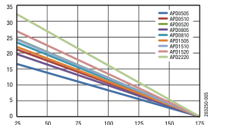
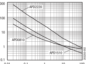
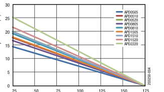
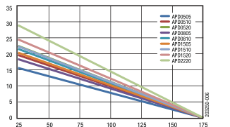
ideal. The absolute maximum ratings of the APD diode series are provided in Table 1. Electrical specifications are provided in Table 2. Typical performance characteristics are provided in Figures 1 through 6.
Page 2
Table 1. APD Series Absolute Maximum Ratings1
| Parameter | Symbol | Minimum | Typical | Maximum | Units |
|---|---|---|---|---|---|
| Power dissipation | PDIS | MaximumTJ CaseTemp ThermalResistancejunctiontocase | W | ||
| Reverse voltage | VR | See Voltage Rating column in Table 2 | V | ||
| Forward current | IF | 200 | mA | ||
| Operating temperature | TOP | –65 | +175 | C | |
| Storage temperature | TSTG | –65 | +200 | C |
1 Exposure to maximum rating conditions for extended periods may reduce device reliability. There is no damage to device with only one parameter set at the limit and all other parameters set at or below their nominal value. Exceeding any of the limits listed here may result in permanent damage to the device.
ESD HANDLING: Although this device is designed to be as robust as possible, electrostatic discharge (ESD) can damage this device.
This device must be protected at all times from ESD when handling or transporting. Static charges may easily produce
potentials of several kilovolts on the human body or equipment, which can discharge without detection.
Industry-standard ESD handling precautions should be used at all times.
Table 2. APD Series Electrical Specifications1 (1 of 2) (TOP = +25 C, Unless Otherwise Noted)
| Part Number | Total Capacitance (CT) @ 50 V, (pF) | Total Capacitance (CT) @ 0 V, (pF) | Series Resistance (RS), @ 10 mA, (Ω) | Minority Carrier Lifetime (TL) @ 10 mA (ns) | Voltage Rating2 (V) | I-Region Thickness (μm) | Thermal Resistance (θJC) (C/W) |
|---|---|---|---|---|---|---|---|
| Maximum | Typical | Maximum | Typical | Minimum | Nominal | Maximum | |
| Switching Applications | |||||||
| APD0505-203 | 0.30 | 0.35 | 2.5 | 70 | 50 | 5 | 232 |
| APD0505-210 | 0.30 | 0.35 | 2.5 | 70 | 50 | 5 | 133 |
| APD0505-219 | 0.30 | 0.35 | 2.5 | 70 | 50 | 5 | 201 |
| APD0505-240 | 0.30 | 0.35 | 2.5 | 70 | 50 | 5 | 214 |
| APD0510-203 | 0.35 | 0.40 | 1.5 | 90 | 50 | 5 | 189 |
| APD0510-210 | 0.35 | 0.40 | 1.5 | 90 | 50 | 5 | 90 |
| APD0510-219 | 0.35 | 0.40 | 1.5 | 90 | 50 | 5 | 158 |
| APD0510-240 | 0.35 | 0.40 | 1.5 | 90 | 50 | 5 | 170 |
| APD0520-203 | 0.40 | 0.45 | 1.0 | 120 | 50 | 5 | 167 |
| APD0520-210 | 0.50 | 0.55 | 1.0 | 120 | 50 | 5 | 59 |
| APD0520-219 | 0.40 | 0.45 | 1.0 | 120 | 50 | 5 | 136 |
| APD0520-240 | 0.40 | 0.45 | 1.0 | 120 | 50 | 5 | 148 |
| APD0805-203 | 0.30 | 0.35 | 2.0 | 100 | 100 | 8 | 201 |
| APD0805-210 | 0.35 | 0.40 | 2.0 | 100 | 100 | 8 | 107 |
| APD0805-219 | 0.30 | 0.35 | 2.0 | 100 | 100 | 8 | 170 |
| APD0805-240 | 0.30 | 0.35 | 2.0 | 100 | 100 | 8 | 182 |
Page 3
Table 2. APD Series Electrical Specifications1 (2 of 2) (TOP = +25 C, Unless Otherwise Noted)
| Part Number | Total Capacitance (CT) @ 50 V, (pF) | Total Capacitance (CT) @ 0 V, (pF) | Series Resistance (RS), @ 10 mA, (Ω) | Minority Carrier Lifetime (TL) @ 10 mA (ns) | Voltage Rating2 (V) | I-Region Thickness (μm) | Thermal Resistance (θJC) (C/W) |
|---|---|---|---|---|---|---|---|
| Maximum | Typical | Maximum | Typical | Minimum | Nominal | Maximum | |
| Switching Applications (continued) | |||||||
| APD0810-203 | 0.35 | 0.40 | 1.5 | 160 | 100 | 8 | 174 |
| APD0810-210 | 0.40 | 0.45 | 1.5 | 160 | 100 | 8 | 75 |
| APD0810-219 | 0.35 | 0.40 | 1.5 | 160 | 100 | 8 | 143 |
| APD0810-240 | 0.35 | 0.40 | 1.5 | 160 | 100 | 8 | 155 |
| APD1505-203 | 0.40 | 0.45 @ 10 V | 2.5 | 350 | 200 | 15 | 172 |
| APD1505-210 | 0.40 | 0.45 @ 10 V | 2.5 | 350 | 200 | 15 | 74 |
| APD1505-219 | 0.40 | 0.45 @ 10 V | 2.5 | 350 | 200 | 15 | 142 |
| APD1505-240 | 0.40 | 0.45 @ 10 V | 2.5 | 350 | 200 | 15 | 150 |
| APD1510-203 | 0.35 | 0.40 | 2.0 | 300 | 200 | 15 | 168 |
| APD1510-210 | 0.35 | 0.40 | 2.0 | 300 | 200 | 15 | 70 |
| APD1510-219 | 0.35 | 0.40 | 2.0 | 300 | 200 | 15 | 137 |
| APD1510-240 | 0.35 | 0.40 | 2.0 | 300 | 200 | 15 | 149 |
| APD1520-203 | 0.40 | 0.45 | 1.2 | 900 | 200 | 15 | 155 |
| APD1520-210 | 0.40 | 0.45 | 1.2 | 900 | 200 | 15 | 57 |
| APD1520-219 | 0.45 | 0.50 | 1.2 | 900 | 200 | 15 | 124 |
| APD1520-240 | 0.40 | 0.45 | 1.2 | 900 | 200 | 15 | 136 |
| Attenuator Applications | |||||||
| APD2220-203 | 0.45 | 0.50 | 4.0 | 100 | 100 | 50 | 132 |
| APD2220-210 | 0.45 | 0.50 | 4.0 | 100 | 100 | 50 | 32 |
| APD2220-219 | 0.40 | 0.45 | 4.0 | 100 | 100 | 50 | 104 |
| APD2220-240 | 0.40 | 0.45 | 4.0 | 100 | 100 | 50 | 115 |
1 Performance is guaranteed only under the conditions listed in this table. 2 Reverse current is specified at 10 μA maximum at the voltage rating noted. Do not exceed this voltage.
Page 4
Typical Performance Characteristics at 25 °C
0.01 0.1 1 10 100
Forward Current (mA)
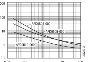
Figure 1. Resistance vs Forward Current @ 1 GHz
25 50 75 100 125 150 175
Case Temperature (°C)
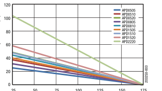
Figure 3. Maximum CW Input Power vs Case Temperature
(-210 Package)
Case Temperature (°C)
Figure 5. Maximum CW Input Power vs Case Temperature
(-219 Package)
0.01 0.1 1 10 100
Forward Current (mA)
Figure 2. Resistance vs Forward Current @ 1 GHz
Case Temperature (°C)
Figure 4. Maximum CW Input Power vs Case Temperature
(-203 Package)
Case Temperature (°C)
Figure 6. Maximum CW Input Power vs Case Temperature
(-240 Package)
Page 5
Package Outline Drawings
Hermetic package outline dimension drawings are shown in Figures 7 through 10.
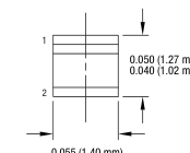
Schematic N-Type 1
2
0.055 (1.40 mm) 0.051 (1.30 mm) Dia.
Dimensions are in inches (millimeters shown in parentheses)
203250-007
Figure 7. -203 Package
Schematic 1
0.064 (1.63 mm)
0.124 (3.15 mm) 0.119 (3.02 mm) Dia.
0.060 (1.52 mm)
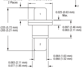
Dimensions are in inches (millimeters shown in parentheses)
203250-008
Figure 8. -210 Package
Page 6
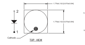
Version A
Schematic
1
0.075 (1.91 mm) 0.065 (1.65 mm) Sq.
Cathode
0.033 (0.84 mm) Min.
1 2
0.010 (0.25 mm) Ref.
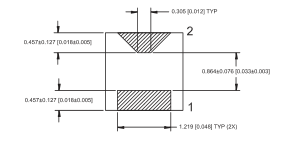
2
0.020 (0.51 mm) Typ.
0.045 (1.14 mm) 0.030 (0.76 mm)
Dimensions are in inches (millimeters shown in parentheses)
Version B
203250-009
Figure 9. -219 Package
Page 7
Schematic
2
1
Colored Dot Denotes Cathode
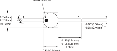
0.104 (2.64 mm) 0.092 (2.34 mm)
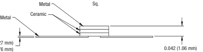
0.005 (0.127 mm) 0.003 (0.076 mm)
0.028 (0.71 mm)
Dimensions are in inches (millimeters shown in parentheses)
203250-010
Figure 10. -240 Package
Page 8
Copyright © 2014, 2017 Isolink, Inc. All Rights Reserved.
Information in this document is provided in connection with Isolink, Inc. (“Isolink”), a wholly-owned subsidiary of Skyworks Solutions, Inc. These materials, including the information contained herein, are provided by Isolink as a service to its customers and may be used for informational purposes only by the customer. Isolink assumes no responsibility for errors or omissions in these materials or the information contained herein. Isolink may change its documentation, products, services, specifications or product descriptions at any time, without notice. Isolink makes no commitment to update the materials or information and shall have no responsibility whatsoever for conflicts, incompatibilities, or other difficulties arising from any future changes.
No license, whether express, implied, by estoppel or otherwise, is granted to any intellectual property rights by this document. Isolink assumes no liability for any materials, products or information provided hereunder, including the sale, distribution, reproduction or use of Isolink products, information or materials, except as may be provided in Isolink Terms and Conditions of Sale.
THE MATERIALS, PRODUCTS AND INFORMATION ARE PROVIDED “AS IS” WITHOUT WARRANTY OF ANY KIND, WHETHER EXPRESS, IMPLIED, STATUTORY, OR OTHERWISE, INCLUDING FITNESS FOR A PARTICULAR PURPOSE OR USE, MERCHANTABILITY, PERFORMANCE, QUALITY OR NON-INFRINGEMENT OF ANY INTELLECTUAL PROPERTY RIGHT; ALL SUCH WARRANTIES ARE HEREBY EXPRESSLY DISCLAIMED. ISOLINK DOES NOT WARRANT THE ACCURACY OR COMPLETENESS OF THE INFORMATION, TEXT, GRAPHICS OR OTHER ITEMS CONTAINED WITHIN THESE MATERIALS. ISOLINK SHALL NOT BE LIABLE FOR ANY DAMAGES, INCLUDING BUT NOT LIMITED TO ANY SPECIAL, INDIRECT, INCIDENTAL, STATUTORY, OR CONSEQUENTIAL DAMAGES, INCLUDING WITHOUT LIMITATION, LOST
REVENUES OR LOST PROFITS THAT MAY RESULT FROM THE USE OF THE MATERIALS OR INFORMATION, WHETHER OR NOT THE RECIPIENT OF MATERIALS HAS BEEN ADVISED OF THE POSSIBILITY OF SUCH DAMAGE.
Customers are responsible for their products and applications using Isolink products, which may deviate from published specifications as a result of design defects, errors, or operation of products outside of published parameters or design specifications. Customers should include design and operating safeguards to minimize these and other risks. Isolink assumes no liability for applications assistance, customer product design, or damage to any equipment resulting from the use of Isolink products outside of stated published specifications or parameters.
Isolink is a trademark of Isolink Inc. in the United States and other countries. Skyworks and the Skyworks symbol are trademarks or registered trademarks of Skyworks Solutions, Inc., in the United States and other countries. Third-party brands and names are for identification purposes only, and are the property of their respective owners.