

 Download PDF
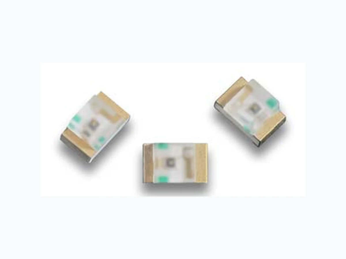
AP2012P3C-P22 KINGBRIGHT
Document overview
- Manufacturer or author: Provided By digicamel.com
- PDF pages: 4
Technical content
© 2017 Kingbright. All Rights Reserved. Spec No: DSAO8747 / 1203000140 Rev No: V.4 Date: 11/20/2017 Page 1 / 4
DESCRIPTION
z Made with NPN silicon phototransistor chips
FEATURES
z 2.0 mm x 1.25 mm SMD LED, 1.1 mm thickness z Mechanically and spectrally matched to the infrared emitting LED lamp z Water clear lens z Package: 2000 pcs / reel z Moisture sensitivity level: 3 z RoHS compliant
APPLICATIONS
z Infrared applied systems z Optoelectronic switches z Photodetector control circuits z Sensor technology PACKAGE DIMENSIONS AP2012P3C-P22 2.0 x 1.25 mm Phototransistor RECOMMENDED SOLDERING PATTERN (units : mm; tolerance : ± 0.1) Notes: 1. All dimensions are in millimeters (inches). 2. Tolerance is ±0.1(0.004") unless otherwise noted. 3. The specifications, characteristics and technical data described in the datasheet are subject to change without prior notice. 4. The device has a single mounting surface. The device must be mounted according to the specifications. Note: 1. Relative humidity levels maintained between 40% and 60% in production area are recommended to avoid the build-up of static electricity – Ref JEDEC/JESD625-A and JEDEC/J-STD-033. ABSOLUTE MAXIMUM RATINGS at TA=25°C Parameter Units Collector-to-Emitter Voltage V Emitter-to-Collector Voltage V Power Dissipation at(or below) 25°C Free Air Temperature mW Operating Temperature °C Storage Temperature °C Max.Ratings 100 -40 to +85 -40 to +85 Confidential
© 2017 Kingbright. All Rights Reserved. Spec No: DSAO8747 / 1203000140 Rev No: V.4 Date: 11/20/2017 Page 2 / 4 ELECTRICAL / OPTICAL CHARACTERISTICS at TA=25°C AP2012P3C-P22 Parameter Symbol Min. Typ. Max. Units Test Conditions Collector-to-Emitter Breakdown Voltage V BR CEO 30 - - V IC = 100uA Ee = 0mW/cm2 Emitter-to-Collector Breakdown Voltage VBR ECO 5 - - V IE = 100uA Ee = 0mW/cm2 Collector-to-Emitter Saturation Voltage VCE (SAT) - - 0.8 V IC = 2mA Ee = 20mW/cm2 Collector Dark Current ICEO - - 100 nA VCE = 10V Ee = 0mW/cm2 Rise Time(10% to 90%) TR - 15 - µS VCE = 5V IC = 1mA RL = 1000Ω Fall Time(90% to 10%) TF - 15 - µS On State Collector Current I(ON ) 0.2 0.4 - mA VCE = 5V Ee = 1mW/cm2 λ = 940nm Range of spectral bandwidth λ0.1 420 - 1120 nm - Wavelength of peak sensitivity λp - 940 - nm - Angle of half sensitivity 2θ1/2 - 160 - deg - 0.5 0.5 90° 15°0° 30° 45° 60° 75° -15° -30° -45° -60° -75° -90° 0.01.0 1.0 Ta = 25 °C Relative sensitivity 20% 40% 60% 80% 100% 350 450 550 650 750 850 950 1050 1150 Ta = 25 °C Wavelength (nm) Relative spectral sensitivity (a. u.) RELATIVE SPECTRAL SENSITIVITY vs. WAVE- RELATIVE RADIANT SENSITIVITY vs. ANGULAR DISPLACEMENT Confidential
© 2017 Kingbright. All Rights Reserved. Spec No: DSAO8747 / 1203000140 Rev No: V.4 Date: 11/20/2017 Page 3 / 4 TECHNICAL DATA AP2012P3C-P22 0.01 0.1 0 5 10 15 20 25 30 Ta = 25 °C Collector-emitter voltage VCE (V) Collector dark current (nA)0.1 100 1000 0 25 50 75 100 VCE = 20V Ee = 0 Ambient temperature (°C) Collector dark current (nA) PHOTOTRANSISTOR 0.1 0.2 0.3 0.4 0.5 012345 Ta = 25 °C Collector-emitter voltage VCE (V) Collector currennt (mA) Ee = 0.25mW/cm2 Ee = 0.5mW/cm2 Ee = 1mW/cm2 100 125 -25 0 25 50 75 100 Ambient temperature (°C) Collector power dissipation Pd (mW) 0.01 0.1 0.01 0.1 1 10 VCE=5V Ta = 25 °C Irradiance Ee (mW/cm2) Collector current Ic (mA) 100 120 140 160 0 1 02 03 04 05 06 07 0 VCE=5V Ee=1mW/cm2 Ambient temperature (°C) Relative collector current (%) Collector Current vs. Irradiance Relative Collector Current vs. Ambient Temperature Collector Dark Current vs. Ambient Temperature Collector Current vs. Collector-Emitter Voltage Collector Power Dissipation vs. Ambient Temperature Collector Dark Current vs. Collector-Emitter Voltage TAPE SPECIFICATIONS (units : mm) REEL DIMENSION (units : mm) REFLOW SOLDERING PROFILE for LEAD-FREE SMD PROCESS Notes: 1. Don't cause stress to the LEDs while it is exposed to high temperature. 2. The maximum number of reflow soldering passes is 2 times. 3. Reflow soldering is recommended. Other soldering methods are not recommended as they might cause damage to the product. Confidential
© 2017 Kingbright. All Rights Reserved. Spec No: DSAO8747 / 1203000140 Rev No: V.4 Date: 11/20/2017 Page 4 / 4 PACKING & LABEL SPECIFICATIONS AP2012P3C-P22 PRECAUTIONARY NOTES 1. The information included in this document reflects representative usage scenarios and is intended for technical reference on ly. 2. The part number, type, and specifications mentioned in this document are subject to future change and improvement without notice. Before production usage customer should refer to the latest datasheet for the updated specifications. 3. When using the products referenced in this document, please make sure the product is being operated within the environmental and electrical limits specified in the datasheet. If customer usage exceeds the specified limits, Kingbright will not be responsible for any subsequent issues. 4. The information in this document applies to typical usage in consumer electronics applications. If customer's application has special reliability requirements or have life-threatening liabilities, such as automotive or medical usage, please consult with Kingbright representative for further assistance. 5. The contents and information of this document may not be reproduced or re-transmitted without permission by Kingbright. 6. All design applications should refer to Kingbright application notes available at http://www.KingbrightUSA.com/ApplicationNotes Confidential