
DATASHEET SEARCH SITE
Document overview
- Manufacturer or author: Provided By digicamel.com
- PDF pages: 11
Technical content
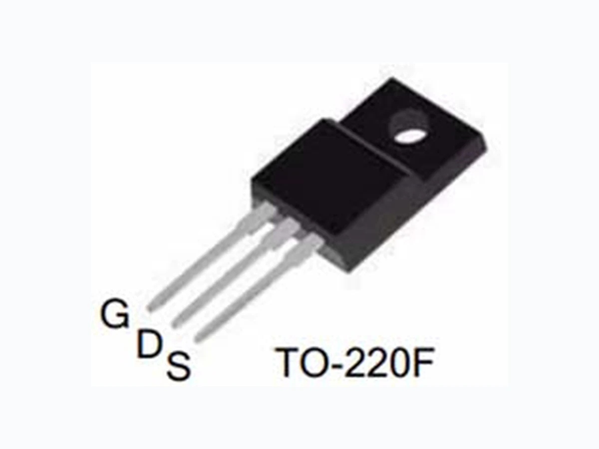
AiT Semiconductor Inc. AM10N65 www.ait-ic.com MOSFET 650V, 10A N-CHANNEL REV1.0 - JUN 2022 RELEASED - - 1 - DESCRIPTION FEATURE The AM10N65 is available in TO-220 and TO220F Packages.
- RDS(ON),typ.=0.75 Ω@VGS=10V
- Low Gate Charge Minimize Switching Loss
- Fast Recovery Body Diode
APPLICATIONS
- Adaptor
- Charger
- SMPS Standby Power ORDERING INFORMATION PIN DESCRIPTION Package Type Part Number TO-220 SPQ: 50pcs/Tube T3 AM10N65T3U AM10N65T3VU TO220F SPQ: 50pcs/ Tube T3F AM10N65T3FU AM10N65T3FVU Note V: Halogen free Package U: Tube AiT provides all RoHS products Pin# Symbol Function
1 G Gate
2 D Drain
3 S Source
AiT Semiconductor Inc. AM10N65 www.ait-ic.com MOSFET 650V, 10A N-CHANNEL REV1.0 - JUN 2022 RELEASED - - 2 - ABSOLUTE MAXIMUM RATINGS TA = 25°C, unless otherwise specified. Parameter Symbol TO-220 TO-220F Unit Drain-to-Source Voltage V DSS 650 V Gate-to-Source Voltage V GSS ± 3 0 Continuous Drain Current I D 1 0 A Pulsed Drain Current at VGS=10V I DM 4 0 Single Pulse Avalanche Energy E AS 800 Power Dissipation PD 125 45 mJ Derating Factor above 25℃ 1.0 0.36 W Soldering Temperature Distance of 1.6mm from case for 10 seconds TL 300 W/℃ Operating and Storage Temperature Range T J &TSTG -55 to 150 ℃ THERMAL RESISTANCE Parameter Symbol TO-220 TO-220F Unit Thermal Resistance, Junction-to-Case RθJC 1.0 2.78 o C/W Thermal Resistance, Junction-to-Ambient R θJA 62 100 Stresses above may cause permanent damage to the device. These are stress ratings only and functional operation of the device at these or any other conditions beyond thos e indicated in the Electrica l Characteristics are not impli ed. Exposure to absolute maximum rating conditions for extended periods may affect device reliability.
AiT Semiconductor Inc. AM10N65 www.ait-ic.com MOSFET 650V, 10A N-CHANNEL REV1.0 - JUN 2022 RELEASED - - 3 -
ELECTRICAL CHARACTERISTICS
TA = 25°C, unless otherwise specified. Parameter Symbol Conditions Min. Typ. Max. Unit OFF CHARACTERISTICS Drain-to-Source Breakdown Voltage BV DSS V GS=0V, ID=250uA 650 - - V Drain-to-Source Leakage Current I DSS VDS=650V, VGS=0V - - 1 uA VDS=520V, VGS=0V, TA =125℃ - - 100 Gate-to-Source Leakage Current I GSS VGS=+30V, VDS=0V - - +100 nA VGS=-30V, VDS=0V - - -100 ON CHARACTERISTICS Static Drain-to-Source On-Resistance RDS(ON) V GS=10V, ID=5.0A - 0.75 0.90 Ω Gate Threshold Voltage, V GS(TH) V DS=VGS, ID=250uA 2.0 - 4.0 V Forward Transconductance gfs V DS=15V, ID=5.0A - 8.0 - S Dynamic CHARACTERISTICS Input Capacitance C iss VGS=0V, VDS=25V, f=1.0MHZ - 1660 - pF Reverse Transfer Capacitance C rss - 1 5 - Output Capacitance C oss - 130 - Total Gate Charge Q g VDD=520V, ID=10A, VGS=0 to 10V - 32 - nC Gate-to-Source Charge Q gs - 8 . 0 - Gate-to-Drain (Miller) Charge Q gd - 8 . 5 - Resistive Switching CHARACTERISTICS Turn-on Delay Time t d(ON) VDD=325V, ID=10A, VGS= 10V RG=4.7Ω - 11 - nS Rise Time t rise - 1 5 - Turn-Off Delay Time t d(OFF) - 4 0 - Fall Time t fall - 1 7 - Source-Drain Diode CHARACTERISTICS Continuous Source Current* I SD Integral PN-diode in MOSFET - - 10 A Pulsed Source Current* I SM - - 4 0 Diode Forward Voltage V SD I S=10A, VGS=0V - - 1.5 V Reverse Recovery Time t rr VGS=0V, IF= IS, di/dt=100A/μs - 460 - ns Reverse Recovery Charge Q rr - 1 . 5 - u C * Pulse width≤380µs; duty cycle≤2%
AiT Semiconductor Inc. AM10N65 www.ait-ic.com MOSFET 650V, 10A N-CHANNEL REV1.0 - JUN 2022 RELEASED - - 4 - TYPICAL PERFORMANCE CHARACTERISTICS Fig 1. Maximum Transient Thermal Impedance Fig 2. Max.Power Dissipation vs Case Temperature Fig 3. Maximum Continuous Drain Current Vs Tc Fig 4. Output Characteristics Fig 5. Rdson vs Gate Voltage
AiT Semiconductor Inc. AM10N65 www.ait-ic.com MOSFET 650V, 10A N-CHANNEL REV1.0 - JUN 2022 RELEASED - - 5 - Fig 6. Peak Current Capability Fig 7. Transfer Characteristics Fig 8. Unclamped Inductive Swit ching Capability Fig 9.Drain to Source ON Resistance Vs Drain Current Fig 10. Rdson vs Junction Temperature
AiT Semiconductor Inc. AM10N65 www.ait-ic.com MOSFET 650V, 10A N-CHANNEL REV1.0 - JUN 2022 RELEASED - - 6 - Fig 11. Breakdown Voltage vs Temperature Fig 12. Threshold Volt age vs Temperature Fig 13. Maximum Continuous Drain Current vs Tc Fig 14. Max. Pow er Dissipation vs Tc Fig 15. Peak Current Capability Fig 16. Peak Current Capability
AiT Semiconductor Inc. AM10N65 www.ait-ic.com MOSFET 650V, 10A N-CHANNEL REV1.0 - JUN 2022 RELEASED - - 7 - TEST CIRCUITS AND WAVEFORMS Fig 17. Peak Diode Recovery dv/dt Test Circuit Fig 18. Peak Diode Recovery dv/dt Waveforms
AiT Semiconductor Inc. AM10N65 www.ait-ic.com MOSFET 650V, 10A N-CHANNEL REV1.0 - JUN 2022 RELEASED - - 8 - Fig19. Switching Test Circuit F ig 20. Switching Waveforms Fig 21. Gate Charge Test Circuit Fig 22. Gate Charge Waveform Fig 23. Unclamped Inductive Switching Test Circuit Fig 24. Uncl amped Inductive Switching Waveforms
AiT Semiconductor Inc. AM10N65 www.ait-ic.com MOSFET 650V, 10A N-CHANNEL REV1.0 - JUN 2022 RELEASED - - 9 -
PACKAGE INFORMATION
Dimension in TO-220 (Unit: mm) Symbol Min. Max. A 10.1 10.5 B 15.2 15.6 B1 9.00 9.40 C 4.40 4.60 C1 2.40 3.00 D 1.20 1.40 E 0.70 0.90 F 0.40 0.60 G 1.17 1.37 H 3.30 3.80 L 13.1 13.7 N 2.34 2.74 Q 2.40 3.00 ΦP 3.70 3.90
AiT Semiconductor Inc. AM10N65 www.ait-ic.com MOSFET 650V, 10A N-CHANNEL REV1.0 - JUN 2022 RELEASED - - 10 - Dimension in TO-220F (Unit: mm) Symbol Min. Max. A 9.70 10.30 B 15.50 16.10 B1 8.99 9.39 C 4.40 4.80 C1 2.15 2.55 D 2.50 2.90 E 0.70 0.90 F 0.40 0.60 G 1.12 1.42 H 3.40 3.80 L 12.6 13.6 N 2.34 2.74 Q 3.15 3.55 ΦP 3.00 3.30
AiT Semiconductor Inc. AM10N65 www.ait-ic.com MOSFET 650V, 10A N-CHANNEL REV1.0 - JUN 2022 RELEASED - - 11 - IMPORTANT NOTICE AiT Semiconductor Inc. (AiT) reserves the right to make changes to any its product, specifications, to discontinue any integrated circuit product or service without n otice, and advises its customers to obtain the latest version of relevant information to verify, before placin g orders, that the information being relied on is current. AiT Semiconductor Inc. integrated circuit products are not designed, intended, authorized, or warranted to be suitable for use in life support applications, devices or syste ms or other critical applications. Use of AiT products in such applications is understood to be fully at the r i s k o f t h e c u s t o m e r . A s u s e d h e r e i n m a y involve potential risks of death, personal injury, or server pr o p e r t y , o r e n v i r o n m e n t a l d a m a g e . I n o r d e r t o minimize risks associated with the customer's applications, the customer should provide adequate design and operating safeguards. AiT Semiconductor Inc. assumes t o no liability to customer prod uct design or application support. AiT warrants the performance of its products of the specifications applicable at the time of sale.