Download PDF
ALD1000 BURR-BROWN
Document overview
- PDF pages: 14
Technical content
Page 1
Precision Programmable
CURRENT/VOLTAGE TRANSMITTER
FEATURES
G SWITCHABLE OUTPUT ±10V OR 4-20mA G DRIVES 1000Ω || 1µF AT 20mA G VOLTAGE AND CURRENT SENSE G GROUND NOISE SUPPRESSION G ERROR DETECTION FLAG G OUTPUT DISABLE G ACCURACY: 0.05% max G WIDE SUPPLY RANGE: ±11V TO +24/–15V
DESCRIPTION
This product is a monolithic programmable voltage-to- current or voltage-to-voltage analog line driver circuit. It can convert a ±10V input into either an output voltage or current with remote sensing. It provides drive for external transistors to boost output current to greater than ±25mA levels. Current and voltage sensing can be performed simultaneously. Current sensing is achieved through a single external sense resistor. Voltage sensing is performed directly across the load. The logic inputs provide for both output disable and switching between constant current or constant voltage output functions. An open collector output provides an error flag for open circuit
loads. The output disable function allows full control of the output even during power-on and power-off sequencing. The instrumentation amplifiers are de- signed to insure that load noise is not circulated within the control loop.
APPLICATIONS
G PROGRAMMABLE CONTROLLERS G STANDARDIZED OUTPUTS FOR
TERMINATION PANELS
G INDUSTRIAL PROCESS CONTROL G PROGRAMMABLE CURRENT SOURCE G MOTOR CONTROL SYSTEMS G PC AND VME BASED INSTRUMENTATION G CONDITIONER FOR STANDARD SENSOR
OUTPUTS
G TEST EQUIPMENT PIN DRIVER
Voltage Error
Phase Compensation
Indication
V
Phase Sense
Output Disable
External PNP
Input
Drive
Select
100Ω Internal Drive External NPN
VIN2
Drive Open-Loop Gain Control
VIN1
IAs Provide
IA Gain
Closed-Loop
IA1
IA2
Control
Gain Control
Input Over-Voltage Protection
International Airport Industrial Park • Mailing Address: PO Box 11400, Tucson, AZ 85734 • Street Address: 6730 S. Tucson Blvd., Tucson, AZ 85706 • Tel: (520) 746-1111 • Twx: 910-952-1111 Internet: http://www.burr-brown.com/ • FAXLine: (800) 548-6133 (US/Canada Only) • Cable: BBRCORP • Telex: 066-6491 • FAX: (520) 889-1510 • Immediate Product Info: (800) 548-6132
©1996 Burr-Brown Corporation
PDS-1292A
Printed in U.S.A. October, 1996
Page 2
SPECIFICATIONS
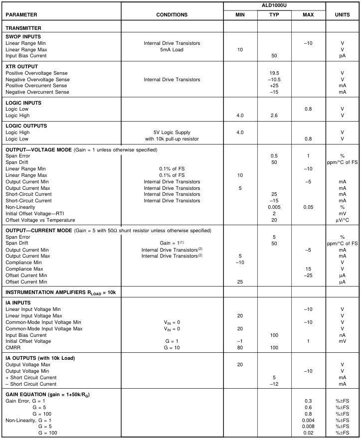
At +VS = 24V, –VS = 15V, TAMB = 25°C, and 2N2222, 2N2907 external transistors, unless otherwise noted.
Page 3
SPECIFICATIONS (CONT)
At +VS = 24V, –VS = 15V, TAMB = 25°C, and 2N2222, 2N2907 external transistors, unless otherwise noted.
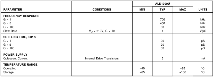
NOTES: (1) Gain drift depends on tempco of 50K factor on gain equation when gain is greater than 1. (2) External Drive capacity varies with configuration. See Application Note.
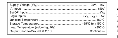
ABSOLUTE MAXIMUM RATINGS
PACKAGE/ORDERING INFORMATION
| PRODUCT | PACKAGE | PACKAGE DRAWING NUMBER(1) |
| ALD1000U | 28-Pin SOIC | 217 |
NOTE: (1) For detailed drawing and dimension table, please see end of data sheet, or Appendix C of Burr-Brown IC Data Book.
ELECTROSTATIC
DISCHARGE SENSITIVITY
This integrated circuit can be damaged by ESD. Burr-Brown
recommends that all integrated circuits be handled with ap-
propriate precautions. Failure to observe proper handling and
installation procedures can cause damage. ESD damage can range from subtle performance degradation
to complete device failure. Precision integrated circuits may
be more susceptible to damage because very small parametric
changes could cause the device not to meet its published
specifications.
The information provided herein is believed to be reliable; however, BURR-BROWN assumes no responsibility for inaccuracies or omissions. BURR-BROWN assumes no responsibility for the use of this information, and all use of such information shall be entirely at the user’s own risk. Prices and specifications are subject to change without notice. No patent rights or licenses to any of the circuits described herein are implied or granted to any third party. BURR-BROWN does not authorize or warrant any BURR-BROWN product for use in life support devices and/or systems.
Page 4
PIN CONFIGURATION
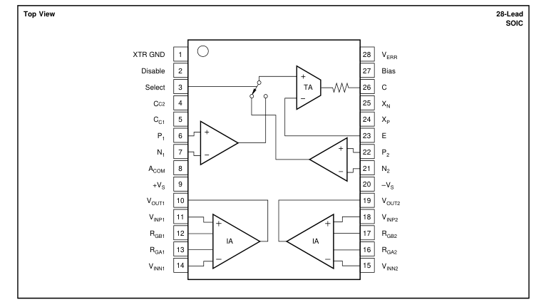
PIN ASSIGNMENTS
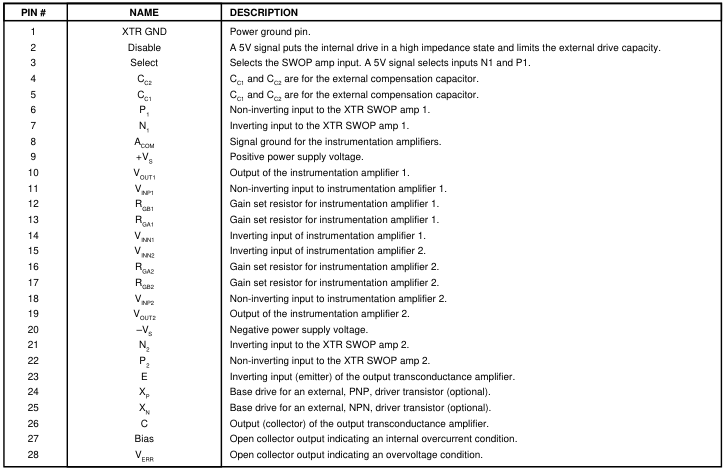
Page 5
TYPICAL PERFORMANCE CURVES
At TA = +25°C; +VS = 24V, –VS = –15V, unless otherwise noted.
STEP RESPONSE IN THE CURRENT FEEDBACK MODE
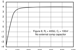
0 100 200 300 400 500 600
Time (µs)
STEP RESPONSE IN VOLTAGE FEEDBACK
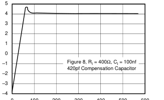
0 100 200 300 400 500 600
Time (µs)
STEP RESPONSE IN CURRENT FEEDBACK MODE
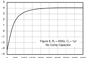
0 500 1000 1500 2000 2500 3000 3500 4000 4500
Time (µs)
STEP RESPONSE IN VOLTAGE FEEDBACK
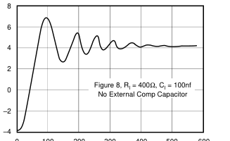
0 100 200 300 400 500 600
Time (µs)
COMPENSATION CAPACITOR vs LOAD CAPACITANCE 1.0E-08
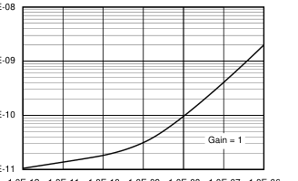
1.0E-09
1.0E-10
1.0E-11 1.0E-12 1.0E-11 1.0E-10 1.0E-09 1.0E-08 1.0E-07 1.0E-06
Load Capacitance
STEP RESPONSE LOAD IN THE VOLTAGE FEEDBACK MODE
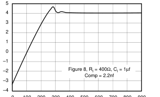
0 100 200 300 400 500 600 700 800 900
Time (µs)
Page 6
TYPICAL PERFORMANCE CURVES (CONT)
At TA = +25°C; +VS = +24V, –VS = –15V, unless otherwise noted.
STEP RESPONSE IN VOLTAGE FEEDBACK MODE
STEP RESPONSE IN CURRENT FEEDBACK MODE
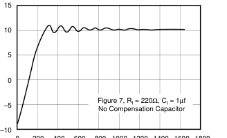
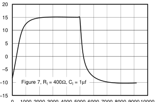
0 200 400 600 800 1000 1200 1400 1600 1800
0 1000 2000 3000 4000 5000 6000 7000 8000 9000 10000
Time (µs)
Time (µs)
STEP RESPONSE IN VOLTAGE FEEDBACK MODE
STEP RESPONSE IN VOLTAGE FEEDBACK MODE
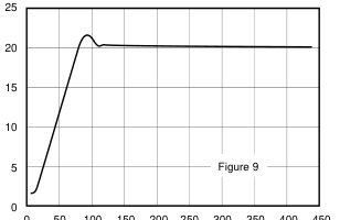
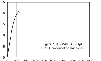
50 100 150 200 250 300 350 400 450
0 200 400 600 800 1000 1200 1400 1600 1800
0
Time (µs)
STEP RESPONSE WITH 2kΩ LOAD CURRENT FEEDBACK
Time (µs)
STEP RESPONSE WITH 2kΩ LOAD VOLTAGE FEEDBACK
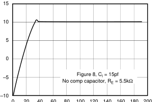
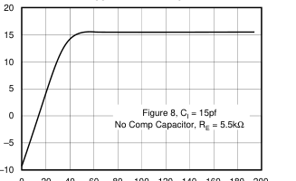
0 20 40 60 80 100 120 140 160 180 200
0 20 40 60 80 100 120 140 160 180 200
Time (µs)
Time (µs)
Page 7
TYPICAL PERFORMANCE CURVES (CONT)
At TA = +25°C; +VS = +24V, –VS = –15V, unless otherwise noted.
COMMON-MODE REJECTION vs FREQUENCY
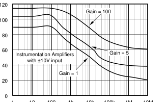
1 10 100 1k 10k 100k
1M 10M
Frequency (Hz)
INPUT BIAS CURRENT vs INPUT VOLTAGE
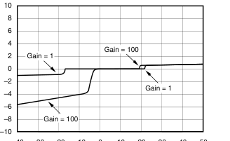
–40 –30 –20 –10 0
10 20 30 40 50 Input Voltage (V)
BASIC OPERATION
ALD1000 FUNCTIONAL BLOCKS
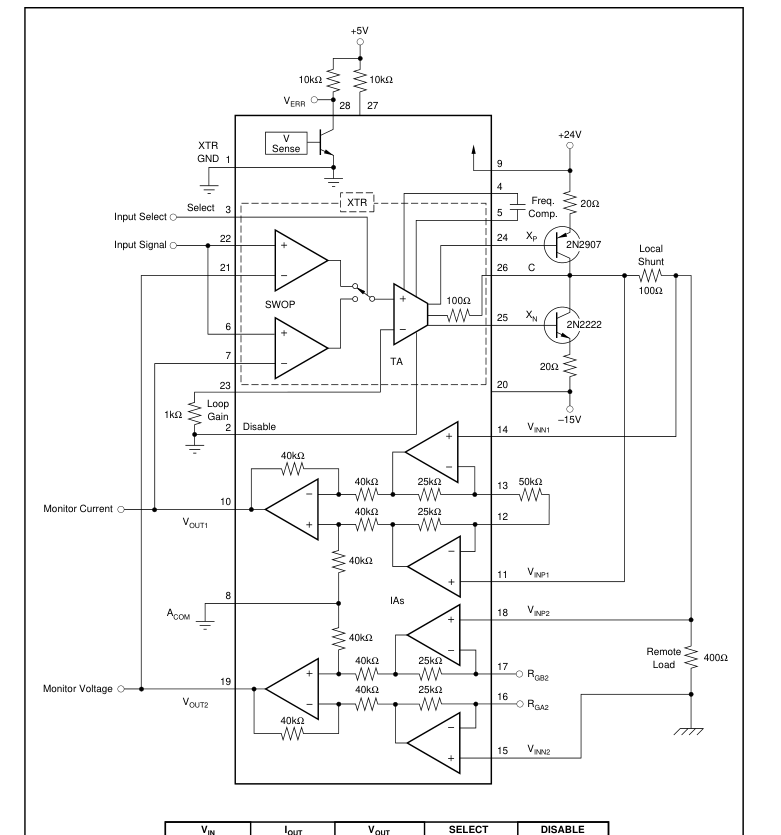
The typical ALD1000 control loop comprises three primary functional blocks (see Figure 1): the current transmitter (XTR), the load, and the instrumentation amplifier (IA). The XTR can be further viewed as divided into the switchable input operational amplifier (SWOP amp), and the voltage to current, transconductance amplifier (TA). Each of these blocks plays a role in the dynamic performance of the control loop, particularly in terms of loop stability with reactive loads.
THE CURRENT TRANSMITTER (XTR)
The XTR produces the forward gain necessary for error amplification. It also controls the frequency response which must be adjusted to balance the trade-off between step response and stability when driving reactive loads. Within the XTR the SWOP amp serves as the input stage. It amplifies the error between the input and output signals to produce a precise signal to the TA to drive the load. The
GAIN vs FREQUENCY
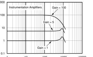
1 10 100 1000 10000
Frequency (kHz)
INPUT COMMON-MODE RANGE vs OUTPUT VOLTAGE
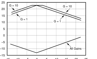
–15 –10 –5
0 5 10 15 20 25
Output Voltage
SWOP amp has two pairs of inputs to provide flexibility of application. The SELECT logic input can switch between two input and feedback signals. Take care, however, to insure that the loop remains stable if switching between current and voltage feedback. The ALD1000 handles a wide range of load conditions in either a voltage or current feedback application. The frequency characteristics of the potential load conditions vary widely. To accommodate these varying frequency characteristics the XTR includes a compensation network. It consists of a simple resistor divider network which forms a single pole, high pass, RC filter when a compensation capacitor is
connected externally. The transconductance amplifier converts the output voltage of the SWOP amp into an output current to drive the load. Whether used in a current feedback or a voltage feedback loop, the ALD1000 transmitter should be viewed as a source of current not voltage. In a voltage loop, the output current is converted to a feedback voltage by the load. In a current loop the output current is converted to a feedback voltage by the shunt resistor. The external, XTR gain resistor, tied to E (Pin 23, Figure 1), sets the voltage to current ratio.
Page 8
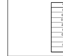
| V IN | I OUT | V OUT | SELECT | DISABLE |
| 0-2 | 0-10mA | 1 | 0 | |
| 0-10 | 0-50mA | 1 | 0 | |
| 0.8-4 | 4-20mA | 1 | 0 | |
| 2-10 | 10-50mA | 1 | 0 | |
| 0-5 | 0-5V | 0 | 0 | |
| 0-10 | 0-10V | 0 | 0 | |
| ±5 | ±5V | 0 | 0 | |
| ±10 | ±10V | 0 | 0 | |
| X | OFF | OFF | X | 1 |
FIGURE 1.
Page 9
THE INSTRUMENTATION AMPLIFIERS (IA)
The ALD1000 includes two, general purpose, uncommitted, 3-op amp, instrumentation amplifiers (see Figure 1). The two IAs are connected to the common power supply and operate at full supply voltage. They share the same analog common reference. Otherwise they are configured independently for maximum flexibility. The instrumentation amplifier senses the feedback signal, reduces any common-mode component, and scales it to the level required. A more comprehensive discussion of the instrumentation amplifiers follows in a later section.
ALD1000 LOGIC
The logic inputs used for the SWOP amp select and the XTR disable functions are simple, differential pair comparators as shown in Figure 2. The logic outputs are open collector NPN transistors with their emitters at ground (pin 1).
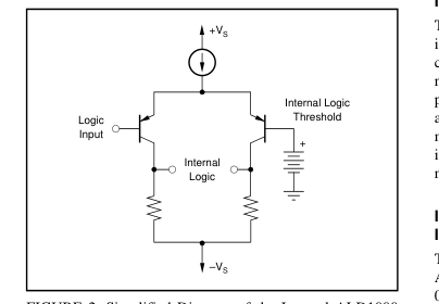
FIGURE 2. Simplified Diagram of the Internal ALD1000 Logic Input Circuitry.
VOLTAGE ERROR INDICATION
The VERR error signal at pin 28 triggers when the voltage at C (pin 26) exceeds the Positive Overvoltage Sense or the Negative Overvoltage Sense (see SPECIFICATIONS) in- ternal thresholds. When external transistors are used without connecting them to C, as shown in Figure 7, the load voltage cannot be detected. The logic signal will generally trigger to an error state (low). However, consider it indeterminate under these conditions.
INSTRUMENTATION
AMPLIFIERS
SETTING THE GAIN
The IA gain is set by connecting a single, external resistor, Rg in Figure 3, between the gain set pins.
G = 1+ 50kΩ RG
INPUT PROTECTION
The inputs of the ALD1000 instrumentation amplifiers are individually protected against over-voltage. Internal circuitry on each input provides low series impedance under normal signal conditions. If the input is overloaded, the protection circuitry limits the input current to a safe value of approximately 1ma to 5ma. Refer to the typical performance curve “Input Bias Current vs Input Voltage.” The inputs are protected even if the power supplies are disconnected or turned off.
IA INPUT OVERLOAD AND
INPUT COMMON-MODE RANGE
The linear voltage range of the input circuitry of the ALD1000 instrumentation amplifiers is from approximately 0.6V below the positive supply to 1V above the negative supply. However, the output swing of the input amplifiers
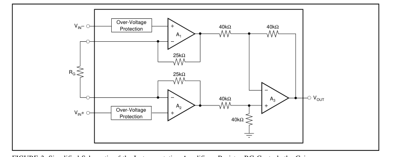
FIGURE 3. Simplified Schematic of the Instrumentation Amplifiers. Resistor RG Controls the Gain.
Page 10
limit this range when a differential input voltage causes the output voltage to increase. Thus, the linear common-mode range relates to the output voltage of the complete amplifier. This behavior also depends in supply voltage—see performance curve “Input Common-Mode Range vs Output Voltage.” The combination of a significant differential signal and a high common-mode voltage as occurs in the current feedback configuration reduces the common-mode range. Ex- ceeding the common-mode range results in a reduced IA output voltage. When this occurs the feedback loop can no longer balance. The forward gain of the ALD1000 amplifies this false error signal, the output voltage tries to increase,
and this holds the IA in an overloaded condition. The ALD1000 applies two defenses against this problem. First, there is a 100Ω resistor in series with the transmitter output. This resistor, which primarily provides protection from over-voltage damage to the output terminal, acts to limit the output swing under high current conditions. Second, the ALD1000’s error detection circuitry signals when the transmitter output voltage exceeds rating. This serves to detect a potential lock condition. Limiting the transmitter’s output swing to within the instrumentation amplifier’s input range allows the loop to recover without reducing the input signal should a transient voltage
level exceed the common-mode input range. However, the common-mode range of the instrumentation amplifiers varies with application specific factors. Lock-up can occur. The application designer must provide defenses against this condition where it is warranted.
USING THE INSTRUMENTATION AMPLIFIERS WITH
A FLOATING SIGNAL SOURCE
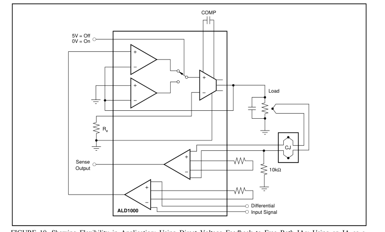
The input impedance of the ALD1000 instrumentation am- plifiers are very high—about 106Ω. Within a feedback loop, as shown in the examples, this characteristic acts to minimize errors caused by loading of the feedback signal. However, if used as an amplifier for a thermocouple, microphone, or other isolated signal source a path is needed for the input bias current. This current is nominally about 100nA. Without a return path the inputs will float to a potential that exceeds the common-mode range of the amplifier. See Figure 10.
LOOP STABILITY
The stability of a closed loop system such as the intended application of the ALD1000 requires adequate phase margin. In contrast, excessive phase margin will reduce the circuit’s transient response to fast changing signals. It is the intent of this section to give an insight into how the ALD1000 circuits blocks affect dynamic performance. Selection of the loop architecture and compensation can then be done em- pirically.
LOOP STABILITY AND THE XTR
There are two critical parameters that must be controlled to
insure adequate transient response and loop stability: loop gain and phase. Together loop gain and phase set the phase margin which defines dynamic performance. Loop gain is the product of the forward voltage to current ratio, the load impedance, and the IA gain. The input error voltage is converted to an output current. The output current is converted to a feedback voltage by the load impedance. The feedback voltage is gained up by the feedback IA. All three blocks affect loop stability. The XTR gain resistor, which is connected to the E pin of the ALD1000, adjusts the voltage to current relationship. In- creasing this resistor decreases loop gain. This, in turn,
increases phase margin and slows step response. This resistor will typically be between 250Ω and 2500Ω. In a voltage feedback loop the frequency at which the loop gain starts to roll off decreases with increasing capacitance. It is necessary to compensate for the loss of bandwidth caused by load capacitance. The compensation network provides this capability. Typical performance curve “Compensation Capacitor vs Load Capacitance” illustrates typical compensation capacitor values for load capacitance varying from 1pf to 1µf. Exact capacitor values will vary with the load resistance, the XTR gain resistor value, IA gain, and variability of the open loop gain of the ALD1000 SWOP
amp. This curve provides a starting point for empirical selection of the compensation capacitor value. The effect described above is much less significant with a current feedback loop since the shunt resistor’s capacitance can be easily controlled. The current feedback loop will be more robust when load conditions are unknown or varying.
LOOP STABILITY AND THE INSTRUMENTATION
AMPLIFIERS
The frequency characteristics and gain of the instrumentation amplifiers affect loop stability when they are used in a feedback loop. There are two main contributions. First, the IA gain directly multiplies loop gain. As a result high IA gains reduce phase margin. Second, when the input exceeds the IA range the IA output can no longer provide the necessary feedback. This can result in a lock condition. Both of these situations are discussed further below.
LOOP GAIN AND THE INSTRUMENTATION
AMPLIFIERS
The ALD1000 is designed for use in a feedback loop. When one of the instrumentation amplifiers is used as the feedback amplifier its gain directly contributes to loop gain. The loop can become unstable if the loop gain is too large. Conversely, it may be possible to stabilize a difficult loop by reducing the gain of the IA. Refer to Figure 4. In this circuit the ALD1000 is configured in a current loop with a 50Ω shunt resistor. A 20ma full scale current through the 50Ω shunt results in a 1V feedback signal. The IA must remove the common-mode level from the shunt voltage and scale the resulting differential signal up to the input signal level.
Page 11
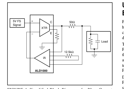
FIGURE 4. Simplified Block Diagram of a 20ma Current Loop. The IA is in a Gain of 5 to Match the 1V Full Scale Shunt Signal to the 5V Full Scale Input Signal.
Here the input signal affects loop stability. A 10V full scale input signal would require an IA gain of 10. A lower input signal, 5V as shown in Figure 4, allows the IA gain to be reduced to 5. This results in a lower loop gain and increased phase margin. Note that it is possible to reduce the IA gain to less than 1 by using a voltage divider at the IA output.
VOLTAGE FEEDBACK AND THE
INSTRUMENTATION AMPLIFIERS
The instrumentation amplifiers can be used for remote sensing in a voltage feedback loop as illustrated in Figure 5. Here the instrumentation amplifier tends to reject small ground potential differences between the source and load. The voltage loop, however, is more sensitive to reactive load impedance than the current loop. The ALD1000 emitter resistor and compensation capacitor need to be selected for the specific load conditions. Voltage feedback may not be appropriate for variable load conditions.
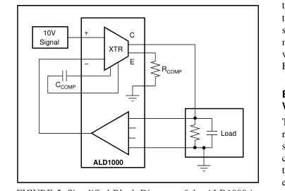
FIGURE 5. Simplified Block Diagram of the ALD1000 in Voltage Feedback.
USING THE ALD1000 WITH
EXTERNAL DRIVE TRANSISTORS
Power dissipated by the internal driver stage affects the built-in instrumentation amplifiers compromising their ac- curacy. External transistors reduce the internal power dissapation. The external transistors are configured as current sources. A PNP transistor delivers positive current. An NPN supplies the negative drive. Either or both can be used. For example a 4ma to 20ma current loop may only require a PNP transistor since negative current drive is not required. See Figure 9. Degeneration resistors are required (refer to R1 and R2 in Figure 6). The value of the degeneration resistors will affect stability, load sharing with the internal driver devices, and
the current limit value. These issues are covered in more detail below.
EXTERNAL TRANSISTORS AND THE CURRENT
LIMIT VALUE
The ALD1000 contains circuitry to prevent damage to the internal components due to excess current. When using the internal driver stage by itself, current to the load is limited to about 20ma at room temperature. When using external drivers, the current limit depends, approximately, on the load sharing ratio between the internal and external transistors. Figure 6 illustrates the circuit relationship between the current limit circuitry and external drive transistors.
THE DEGENERATION RESISTORS
The degeneration resistors, R1 and R2 in Figure 6, control the load sharing between the internal and external transistors. Choose the resistor values by measuring load current, current through the external transistor, and calculating the current being supplied by the internal drive.
LOOP STABILITY AND THE DEGENERATION
RESISTORS
Loop stability depends on loop gain. Because the degeneration resistors affect the voltage to current ratio of the loop the value of these resistors also affect loop gain and thus stability. Smaller resistor values will increase loop gain. It may be necessary to compensate for this by adjusting the value of the XTR gain resistor connected to the E Pin, R4 in Figure 6.
EXTERNAL TRANSISTORS AND OUTPUT
VOLTAGE SWING
The output voltage swing must be limited within the input range of the instrumentation amplifiers. The 100Ω resistor shown in Figure 6 limits output swing under high current conditions. Resistor R3 performs this function with external transistors. R3 must be sized to limit output swing, at the expected full load, within the input range of the instrumentation amplifiers. Refer to the section on the instrumentation amplifiers for further information.
Page 12
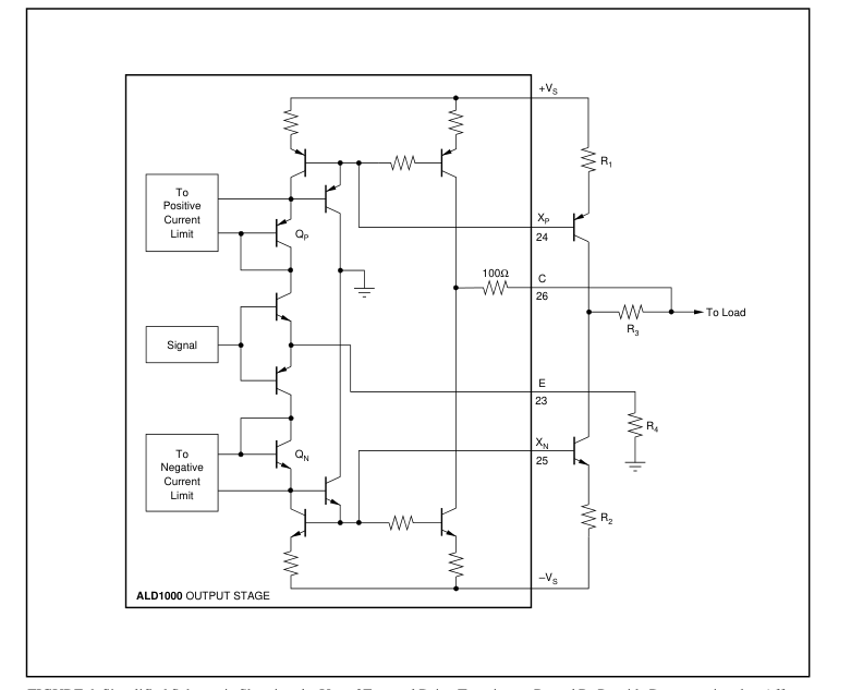
FIGURE 6. Simplified Schematic Showing the Use of External Drive Transistors. R1 and R2 Provide Degeneration that Affects the Current Limit and Loop Stability. R4 Controls the Transconductance Amplifier Gain Affecting Loop Stability and Transient Response. See the Text.
Page 13
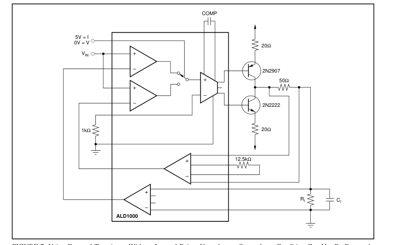
FIGURE 7. Using External Transistors Without Internal Drive. Note that an Overvoltage Condition Can Not Be Detected.
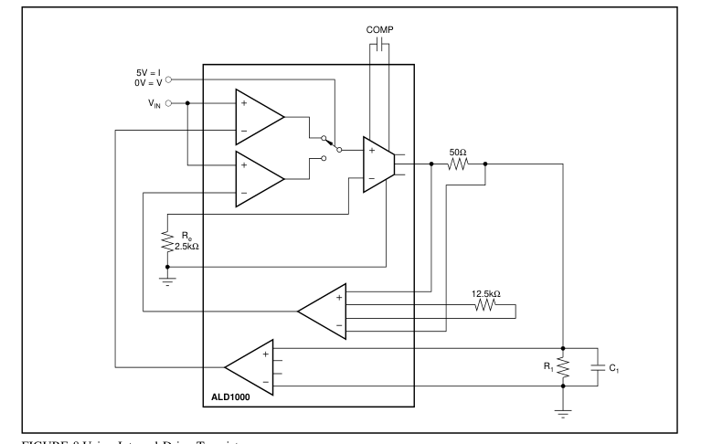
FIGURE 8.Using Internal Drive Transistors.
Page 14
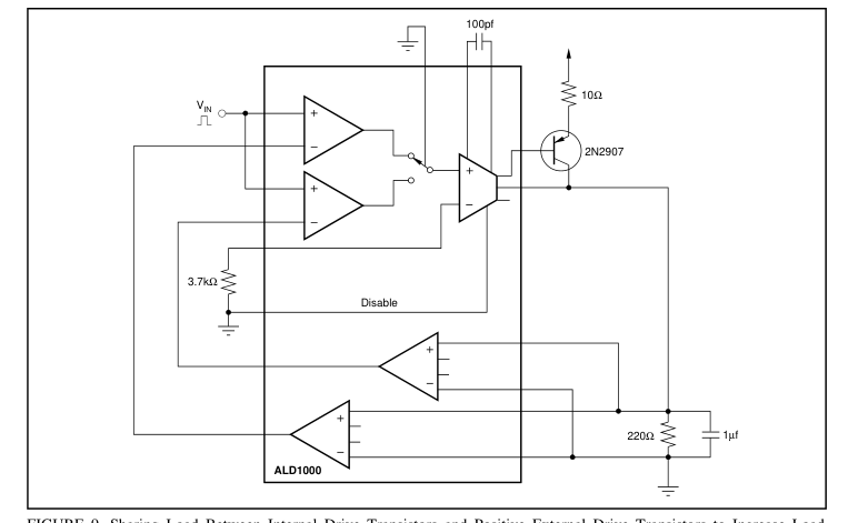
FIGURE 9. Sharing Load Between Internal Drive Transistors and Positive External Drive Transistors to Increase Load
Capacity. A Similiar Configuration is Possible with the Negative External Drive Transistor.