


 Download PDF
AFE1115 TI1
Document overview
- PDF pages: 14
Technical content
Page 1
SBWS005
Page 2
SPECIFICATIONS
Typical at 25°C, AVDD = +5V, DVDD = +3.3V, ftx = 584kHz (E1 rate), unless otherwise specified.
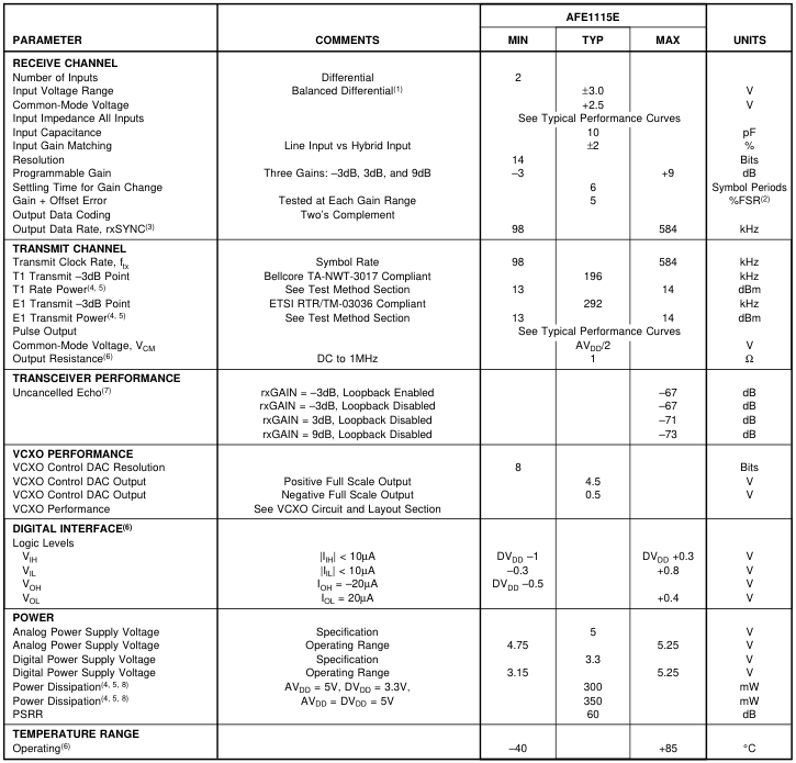
NOTES: (1) With a balanced differential signal, the positive input is 180° out of phase with the negative input, therefore the actual voltage swing about the commonmode voltage on each pin is ±1.5V to achieve a total input range of ±3.0V or 6Vp-p. (2) FSR is Full-Scale Range. (3) The output data is available at twice the symbol rate with interpolated values. (4) With a pseudo-random equiprobable sequence of HDSL pulses; 13.5dBm applied to the transformer (16.5dBm output from txLINEP and txLINEN). (5) See the Test Method section of this data sheet for more information. (6) Guaranteed by design and characterization. (7) Uncancelled Echo is a measure of the total analog errors in the transmitter and receiver sections including the effect of non-linearity and noise. See the Discussion of Specifications sections
of this data sheet for more information. (8) Power dissipation includes only the power dissipated with in the component and does not include power dissipated in the external loads. See the Discussion of Specifications section for more information.
Page 3
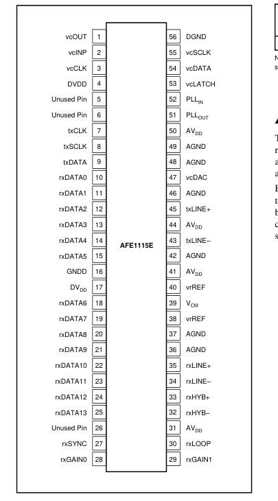
PIN CONFIGURATION
PACKAGE/ORDERING INFORMATION
| PRODUCT | PACKAGE | PACKAGE DRAWING NUMBER(1) | TEMPERATURE RANGE |
| AFE1115E | 56-Pin Plastic SSOP | 346 | –40°C to +85°C |
NOTE: (1) For detailed drawing and dimension table, please see end of data sheet, or Appendix C of Burr-Brown IC Data Book.
ELECTROSTATIC
DISCHARGE SENSITIVITY
This integrated circuit can be damaged by ESD. Burr-Brown recommends that all integrated circuits be handled with appropriate precautions. Failure to observe proper handling and installation procedures can cause damage. ESD damage can range from subtle performance degradation to complete device failure. Precision integrated circuits may be more susceptible to damage because very small parametric changes could cause the device not to meet its published specifications.
Page 4
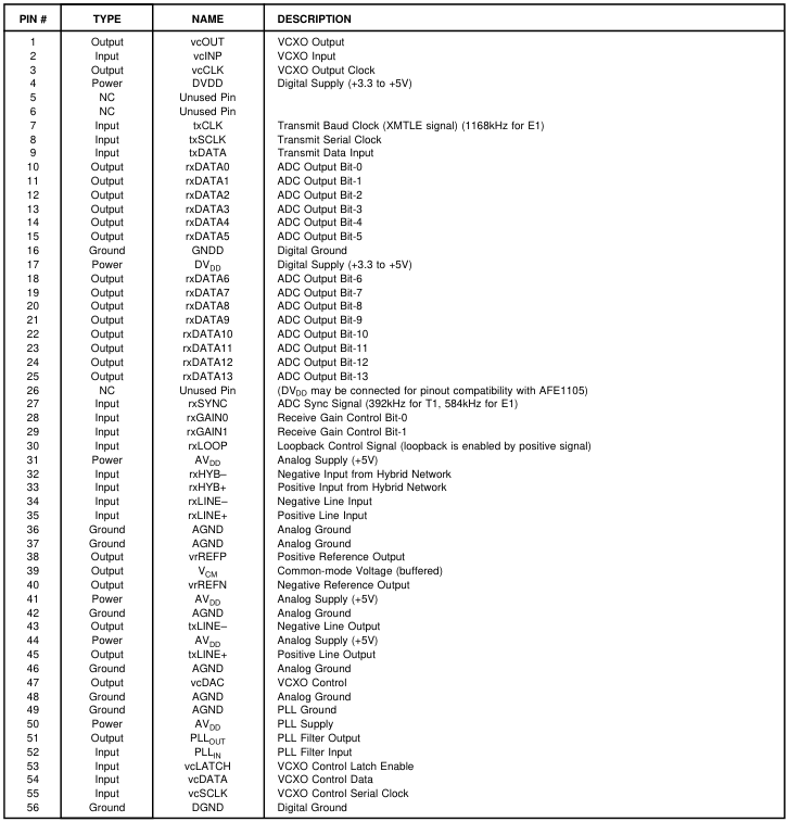
PIN DESCRIPTIONS
The information provided herein is believed to be reliable; however, BURR-BROWN assumes no responsibility for inaccuracies or omissions. BURR-BROWN assumes no responsibility for the use of this information, and all use of such information shall be entirely at the user’s own risk. Prices and specifications are subject to change without notice. No patent rights or licenses to any of the circuits described herein are implied or granted to any third party. BURR-BROWN does not authorize or warrant any BURR-BROWN product for use in life support devices and/or systems.
Page 5
TYPICAL PERFORMANCE CURVES
At Output of Pulse Transformer
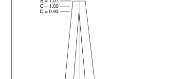
The curves shown below are measured at the line output of the HDSL transformer. Typical at 25°C, AVDD = +5V, DVDD = +3.3V, unless otherwise specified.
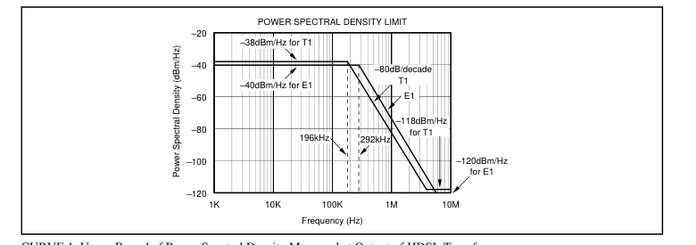
CURVE 1. Upper Bound of Power Spectral Density Measured at Output of HDSL Transformer.
0.4T 0.4T
B = 1.07

| NORMALIZED LEVEL | QUATERNARY SYMBOLS | ||||
|---|---|---|---|---|---|
| +3 | +1 | –1 | –3 | ||
| A B C D L K E F G H | 0.01 1.07 1.0D0 O 0.93 NOWN 0.03 –0.01 –0.16 –0.05 | 0.0264 2.8248 N2'.T64 0D0 E 2.4552 IF TE 0.0792 –0.0264 –0.4224 –0.1320 | 0.0088 0.9416 L0E.88T00E 0.8184 EPLE 0.0264 –0.0088 –0.1408 –0.0440 | –0.0088 –0.9416 T–A0.8B80L0 –0.8184 IS LEA –0.0264 0.0088 0.1408 0.0440 | –0.0264 –2.8248 E –2.6400 –2.4552 VING –0.0792 0.0264 0.4224 0.1320 |
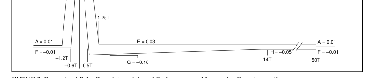
CURVE 2. Transmitted Pulse Template and Actual Performance as Measured at Transformer Output.
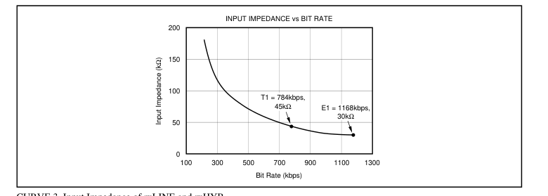
CURVE 3. Input Impedance of rxLINE and rxHYB.
Page 6
THEORY OF OPERATION
The transmit channel consists of a switched-capacitor pulse forming network followed by a differential line driver. The pulse forming network receives symbol data through a serial interface and generates a standard 2B1Q output waveform. The output meets the pulse mask and power spectral density requirements defined in European Telecommunications Standards Institute document RTR/TM-03036 for E1 mode and in sections 6.2.1 and 6.2.2.1 of Bellcore technical advisory TA-NWT-001210 for T1 mode. The differential line driver uses a composite output stage combining class B operation (for high efficiency driving large signals) with class AB operation (to minimize crossover distortion).
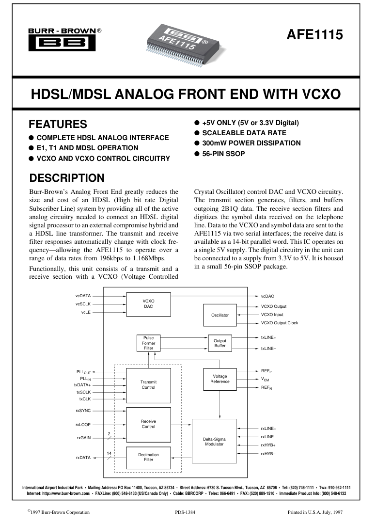
The receive channel is designed around a fourth-order delta sigma A/D converter. It includes a difference amplifier designed to be used with an external compromise hybrid for first order analog echo cancellation. A programmable gain amplifier with gains of –3dB to +9dB is also included. The delta sigma modulator operating at a 24X oversampling ratio produces a parallel 14-bit output at symbol rates up to 584kHz. The basic functionality of the AFE1115 is illustrated in Figure 1 shown below. The receive channel operates by summing the two differential inputs, one from the line (rxLINE) and the other from the compromise hybrid (rxHYB). These two inputs are con-
nected so that the hybrid signal is subtracted from the line signal. This connection is described in the paragraph titled “Echo Cancellation in the AFE”. The equivalent gain for each input in the difference amp is one. The resulting signal then passes to a programmable gain amplifier which can be set for gains of –3dB through +9dB. The ADC converts the signal to a 14-bit digital word, rxD13-rxD0. An independent VCXO control DAC and VCXO circuitry is also included on the chip. This VCXO is designed to be used
in remote units for clock recovery. The VCXO is formed with the on-board circuitry plus external crystal and varactor diodes. The VCXO control DAC receives control data through a serial interface which sets a voltage level at the output of the DAC. The DAC output controls the frequency of the VCXO. To achieve specified analog performance when using the VCXO, the crystal frequency of the VCXO must be 48x the baud rate.
rxLOOP INPUT rxLOOP is the loopback control signal. When enabled, the rxLINE+ and rxLINE– inputs are disconnected from the AFE. The rxHYB+ and rxHYB– inputs remain connected. Loopback is enabled by applying a positive signal (Logic 1) to rxLOOP.
ECHO CANCELLATION IN THE AFE
The rxHYB input is designed to be subtracted from the rxLINE input for first order echo cancellation. To accomplish this, note that the rxLINE input is connected to the same polarity signal at the transformer (positive to positive and negative to negative) while the rxHYB input is connected to opposite polarity through the compromise hybrid (negative to positive and positive to negative) as shown in Figure 2.
RECEIVE DATA CODING
The data from the receive channel A/D converter is coded in two’s complement.

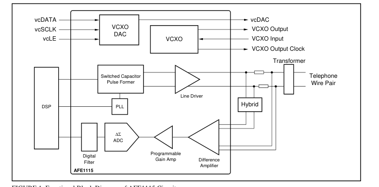
FIGURE 1. Functional Block Diagram of AFE1115 Circuit.
Page 7
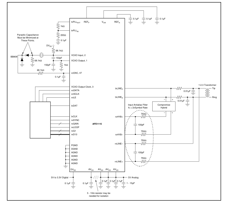
FIGURE 2. Basic Connection Diagram.
RECEIVE CHANNEL PROGRAMMABLE
GAIN AMPLIFIER
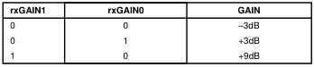
The gain of the amplifier at the input of the Receive Channel is set by two gain control pins, rxGAIN1 and rxGAIN0. The resulting gain between –3dB and +9dB is shown below.
SCALEABLE DATA RATE
The AFE1115 scales operation with the clock frequency. All internal filters and the pulse former change frequency with the clock speed so that the unit can be used at different frequencies just by changing the clock speed.
rxHYBAND rxLINE INPUT ANTI-ALIASING FILTERS An external input anti-aliasing filter is needed on the hybrid and line inputs as shown in the Basic Connection Diagram above. The –3dB frequency of the input anti-aliasing filter for the rxLINE and rxHYB differential inputs should be approximately 1MHz for E1 and T1 symbol rates. Suggested values for the filter are 750Ω for each of the two input resistors and 100pF for the capacitor. Together the two 750Ω resistors and the 100pF capacitor result in a 3dB frequency of just over 1MHz. The 750Ω input resistors will result in a minimal voltage divider loss with the input impedance of the AFE1115. For speed less than E1, the anti-aliasing filters will give best
performance with 3dB frequency approximately equal to two times the symbol rate. For instance, a 3dB frequency of 400kHz may be used for a single line symbol rate of 196k symbols per second.
Page 8
rxHYB AND rxLINE INPUT COMMON-MODE
OPTIONAL VOLTAGE The AFE1115 will meet specifications with the application
circuit shown in the Basic Connection Diagram (Figure 2)
above. However, slightly improved performance may be
obtained with the Hybrid input (rxHYB) and the Line input
(rxLINE) set to a common mode voltage of 1.5V. The
negative reference output pin (vrREFN, pin 40) provides a
good 1.5V level to use to set the common-mode voltage.
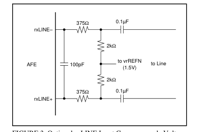
The circuit shown in Figure 3 can be used to set the
common-mode voltage of the Line input to 1.5V. A similar circuit can be used to set the Hybrid input to 1.5V.
Another option for the Hybrid input is to design the external
compromise hybrid so that the signal into the rsHYB inputs
is centered at 1.5V. If the compromise hybrid circuit is AC
FIGURE 3. Optional rxLINE Input Common-mode Voltage
coupled to the rxHYB inputs, an external pull-up resistor to
Control.
vrREFN may be needed to center the input at 1.5V.
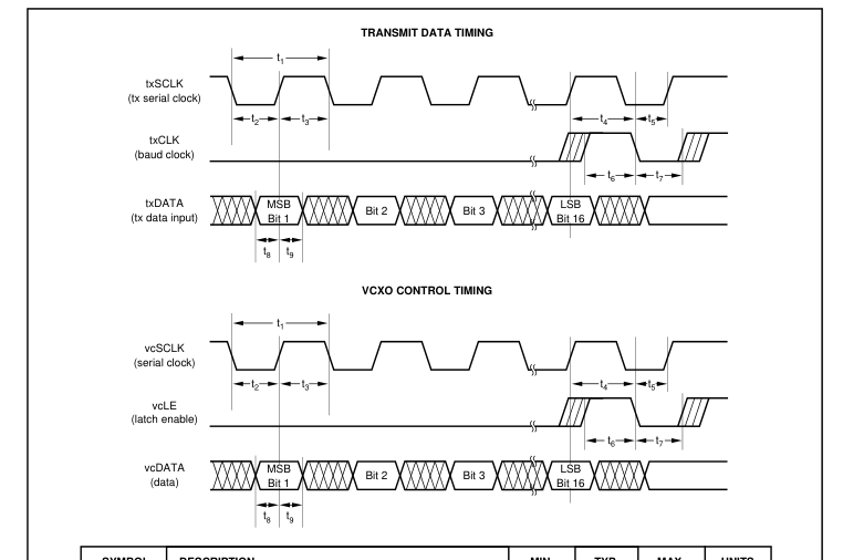
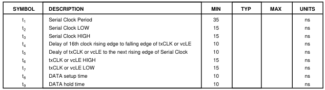
FIGURE 4. Timing Diagram.
Page 9
TRANSMIT SYMBOL DATA During each symbol period transmit symbol data are sent to
the AFE1115 in serial format through the txDATA input pin.
A 16 bit word is sent to the AFE1115 to determine the
symbol that is transmitted by the AFE1115. The symbol data
is contained in the first three bits of the data, the remaining
13 bits of the 16 bit word are ignored. The most significant bit (MSB) is the transmit enable bit.
When the MSB is a logic 0, a zero symbol only is transmit-
ted regardless of the state of the other two bits. When the
MSB is a logic 1, bits 2 and 3 determine the symbol
transmitted as shown in the table below.
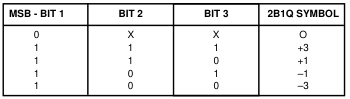
TABLE I. Transmit Symbol Data (txDATA). X = Don’t Care.
VCXO CONTROL D/A CONVERTER DATA During each symbol period VCXO control D/A converter
data is sent to the AFE1115 in serial format through the
vcDATA input pin. A 16 bit word is sent to the AFE1115 to
determine the output of the VCXO control D/A converter.
The VCXO control D/A converter is connected to the
VCXO circuit to control the VCXO frequency. The D/A
converter input is contained in the first eight bits of the data,
the remaining eight bits of the 16 bit word are ignored.
| INPUT CODE (vcDATA) MSB | ANALOG OUTPUT |
| 01111111XXXXXXXX 00000000XXXXXXXX 10000000XXXXXXXX | Negative Full Scale (+0.5V) Mid Scale (+2.5V) Positive Full Scale (+4.5V) |
TABLE II. VCXO Control DAC Output. X = Don’t Care.
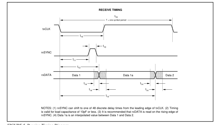
FIGURE 5. Receive Timing Diagram.
| PARAMETER | DESCRIPTION | MIN | TYP | MAX | VALUE |
|---|---|---|---|---|---|
| t 10 t11 t 12 t13 t 14 t 15 t16 | rxSYNC Pulse Width Delay of rxSYNC from rising edge of txCLK, n = 0 to 47 Nominal Time at Which rxDATA Changes from Data 1 to Data 1a Nominal Time at Which rxDATA Changes from Data 1a to Data 2 Uncertainty of t12 and t13 txCLK Pulse Width Symbol Period, T | T/24 nT/48 – T/96 T/16 1.7 | (n + 1.5) T/48 (n + 25.5) T/48 | nT/48 + T/96 20 15T/16 10.2 | ns µs |
TABLE III. Receive Timing (n = Delay Increments from txCLK).
Page 10
RECEIVE TIMING
The rxSYNC signal controls portions of the A/D converter’s decimation filter and the data output timing of the A/D converter. It is generated at the symbol rate by the user and must be synchronized with txCLK. The leading edge of rxSYNC can occur at the leading edge of txCLK or it can be shifted by the user in increments of 1/48 of a symbol period to one of 47 discrete delay times after the leading edge of txCLK. The bandwidth of the A/D converter decimation filter is equal to one half of the symbol rate. The A/D converter data output rate is 2X the symbol rate. The specifications of the AFE1115 assume that one A/D converter output is used per symbol period and the other output is ignored. The Receive
Timing Diagram above suggests using the rxSYNC pulse to read the first data output in a symbol period. Either data output may be used. Both data outputs may be used for more flexible post-processing.
DISCUSSION OF
SPECIFICATIONS
UNCANCELLED ECHO
The key measure of transceiver performance is uncancelled echo. This measurement is made as shown in the diagram of Figure 6 and the measurement is made as follows. The AFE is connected to an output circuit including a typical 1:2.3 line transformer. The line is simulated by a 135Ω resistor.
Symbol sequences are generated by the tester and applied both to the AFE and to the input of an adaptive filter. The output of the adaptive filter is subtracted from the AFE output to form the uncancelled echo signal. Once the filter taps have converged, the RMS value of the uncancelled echo is calculated. Since there is no far-end signal source or additive line noise, the uncancelled echo contains only noise and linearity errors generated in the transmitter and receiver. The data sheet value for uncancelled echo is the ratio of the RMS uncancelled echo (referred to the receiver input through the receiver gain) to the nominal transmitted signal (13.5dBm
into 135Ω, or 1.74Vrms). This echo value is measured under a variety of conditions: with loopback enabled (line input disabled); with loopback disabled under all receiver gain ranges; and with the line shorted (S1 closed in Figure 6).
POWER DISSIPATION
Approximately 75% of the power dissipation in the AFE1115 is in the analog circuitry, and this component does not change with clock frequency. However, the power dissipation in the digital circuitry does decrease with lower clock frequency. In addition, the power dissipation in the digital section is decreased with operation from a smaller supply voltage, such as 3.3V. (The analog supply, must remain in the range 4.75V to 5.25V.) The power dissipation listed in the specifications section applies under these normal operating conditions: 5V Analog Power Supply; 3.3V Digital Power Supply; E1 baud rate;
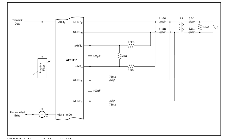
FIGURE 6. Uncancelled Echo Test Diagram.
Page 11
13.5dBm delivered to the line; and a pseudo-random equiprobable sequence of HDSL pulses. The power dissipation specifications includes all power dissipated in the AFE1115, it does not include power dissipated in the external
load.
The external power is 16.5dBm, 13.5dBm to the line and 13.5dBm to the impedance matching resistors. The external load power of 16.5dBm is 45mW. The typical power dissipation in the AFE1115 under various conditions is shown in
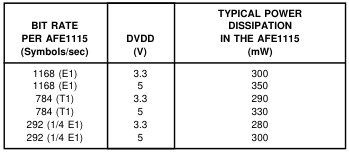
TABLE IV. Typical Power Dissipation.
Table IV.
LAYOUT
The analog front end of an HDSL system has a number of conflicting requirements. It must accept and deliver digital outputs at fairly high rates of speed, generate a VCXO clock, phase-lock to a high-speed digital clock, and convert the line input to a high-precision (14-bit) digital output. Thus, there are really four sections of the AFE1115: the digital section, the phase-locked loop, the VCXO and the analog section.
DIGITAL LAYOUT
The power supply for the digital section of the AFE1115 can range from 3.3V to 5V. This supply should be decoupled to digital ground with a ceramic 0.1µF capacitor placed as close as possible to digital ground (DGND, pin 16) and digital power (DVDD, pin 17). Ideally, both a digital power supply plane and a digital ground plane should run to and underneath the digital pins of the AFE1115 (pins 7 through 30). However, DVDD may be supplied by a wide printed circuit board trance. A digital ground plane underneath all digital pins is strongly recommended. The VCXO circuit needs special attention for layout. There is a portion of the external VCXO circuitry which needs to be as far away as
possible from a ground or power plane or other traces. See the discussion below in the section titled VCXO Circuit and Layout.
ANALOG LAYOUT
The phase-locked loop is powered from AVDD (pin 50) and its ground is referenced to AGND (pin 49). Note that AVDD must be in the 4.75V to 5.25V range. This portion of the AFE1115 should be decoupled with both 10µF Tantalum capacitor and a 0.1µF ceramic capacitor. The ceramic ca- pacitor should be placed as close to the AFE1115 as pos-
sible. The placement of the Tantalum capacitor is not as critical, but should be close to the pin. In each case, the capacitor should be connected between AVDD and AGND (pins 49 and 50). The capacitors should be placed in quiet analog areas rather than noisy digital areas. In most systems, it will be natural to derive AVDD for the phase-locked loop (PLL) from the AVDD supply. A 5Ω to 10Ω resistor should be used to connect PLL AVDD (pin 49) to the analog supply. This resistor in combination with the 10µF capacitor form a lowpass filter—keeping glitches on the analog supply from affecting the phase locked loop. Ideally, the phase-locked loop power supply would originate
from the analog supply (via the 5Ω to 10Ω resistor) near the power connector for the printed circuit board. Likewise, the PLL ground should connect to a large PCB trace or small ground plane which returns to the power supply connector underneath the PLL AVDD supply path. The PLL “ground plane” should also extend underneath PLLIN and PLLOUT (pins 51 and 52). The remaining portion of the AFE1115 should be considered analog. The four non-PLL AGND pins (pins 36, 37, 42, and 46) should be connected directly to a common analog ground plane and all non-PLL AVDD pins should be connected to an analog 5V power plane. Both of these planes should have a low impedance path to the power supply.
Ideally, all ground planes and traces and all power planes and traces should return to the power supply connector before being connected together (if necessary). Each ground and power pair should be routed over each other, should not overlap any portion of another pair, and the pairs should be separated by a distance of at least 0.25 inch (6mm). One exception is that the digital and analog ground planes should be connected together underneath the AFE1115 by a small trace.
VCXO CIRCUIT AND LAYOUT
The VCXO circuitry is shown in Figure 7. The basic VCXO circuit consists of on-chip control DAC, amplifiers, Schmidt triggers, and clock buffer along with an external crystal and varactor diodes. The control DAC output (vcDAC) varies the capacitance of the varactor diodes (D1 and D2), which controls the frequency at which the crystal circuit oscillates. The buffered clock output is available at pin 3, VCXO Clock Output. Important Note: To achieve specified analog performance when using VCXO, the crystal frequency of the VCXO must be 48x the baud rate. In addition, the txCLK and the rxSYNC control signals must be derived from the VCXO clock so that the edges of the control signal are synchronized
with the 48x crystal frequency. If these recommendations are followed, the key internal analog decisions are made at the time of minimum noise. As an example, for an E1 rate of 1168kbps, the symbol rate is 584k symbols per second. In this case the VCXO crystal frequency should be 48 x 584k = 28.032MHz. Likewise, for T1, the crystal frequency should be 18.816MHz.
Page 12
The performance of the VCXO is critically dependent on the
external components and printed circuit board layout that is
used. The varactor diodes and the crystal are particularly
important components. The printed circuit board layout containing the two varactor
diodes, D1 and D2, in the VCXO external circuitry is critical
to the performance of the VCXO. In particular, the two
connection points of the varactor diodes shown in the Figure
7 must have very low parasitic capacitance to ground to
achieve the best tuning range possible. To achieve lowest
parasitic capacitance to ground, there must be no ground
plane or other PCB traces near these two points. Ground
planes and other traces should be kept 1 cm away from these
two points where possible.
Figure 8 shows an example of a printed circuit board layout
of the sensitive VCXO circuitry for the circuit shown in
Figure 7. There should be no ground planes, power planes or
other traces in the white area indicated around the two
sensitive points. The balance of the circuit board should be
covered by ground planes where possible. With the circuit
shown in Figure 7, these typical specifications were achieved.
| Pull Range at 20MHz | ±125ppm |
| Frequency Range of Crystal that can be used | 10MHz to 28MHz |
| Crystal Frequency | 48x baud rate |
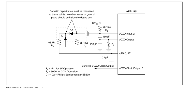
FIGURE 7. VCXO Circuitry.
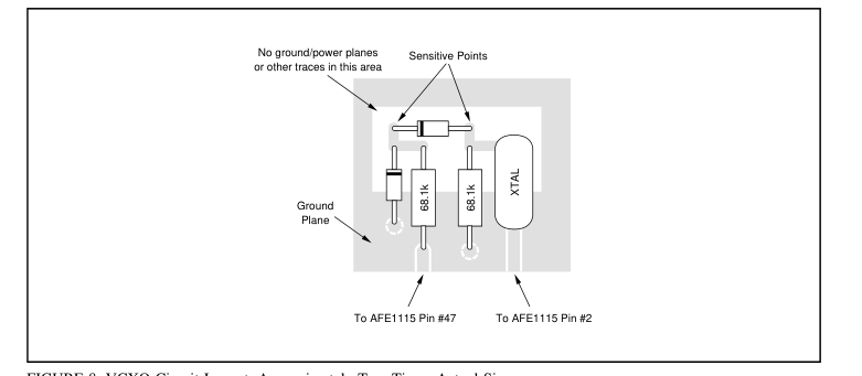
FIGURE 8. VCXO Circuit Layout, Approximately Two Times Actual Size.
Page 13
PACKAGE OPTION ADDENDUM
14-Oct-2008
www.ti.com
PACKAGING INFORMATION

(1) The marketing status values are defined as follows: ACTIVE: Product device recommended for new designs. LIFEBUY: TI has announced that the device will be discontinued, and a lifetime-buy period is in effect. NRND: Not recommended for new designs. Device is in production to support existing customers, but TI does not recommend using this part in a new design. PREVIEW: Device has been announced but is not in production. Samples may or may not be available. OBSOLETE: TI has discontinued the production of the device.
(2) Eco Plan - The planned eco-friendly classification: Pb-Free (RoHS), Pb-Free (RoHS Exempt), or Green (RoHS & no Sb/Br) - please check http://www.ti.com/productcontent for the latest availability information and additional product content details. TBD: The Pb-Free/Green conversion plan has not been defined. Pb-Free (RoHS): TI's terms "Lead-Free" or "Pb-Free" mean semiconductor products that are compatible with the current RoHS requirements for all 6 substances, including the requirement that lead not exceed 0.1% by weight in homogeneous materials. Where designed to be soldered at high temperatures, TI Pb-Free products are suitable for use in specified lead-free processes.
Pb-Free (RoHS Exempt): This component has a RoHS exemption for either 1) lead-based flip-chip solder bumps used between the die and package, or 2) lead-based die adhesive used between the die and leadframe. The component is otherwise considered Pb-Free (RoHS compatible) as defined above. Green (RoHS & no Sb/Br): TI defines "Green" to mean Pb-Free (RoHS compatible), and free of Bromine (Br) and Antimony (Sb) based flame retardants (Br or Sb do not exceed 0.1% by weight in homogeneous material)
(3) MSL, Peak Temp. -- The Moisture Sensitivity Level rating according to the JEDEC industry standard classifications, and peak solder temperature.
Important Information and Disclaimer:The information provided on this page represents TI's knowledge and belief as of the date that it is provided. TI bases its knowledge and belief on information provided by third parties, and makes no representation or warranty as to the accuracy of such information. Efforts are underway to better integrate information from third parties. TI has taken and continues to take reasonable steps to provide representative and accurate information but may not have conducted destructive testing or chemical analysis on incoming materials and chemicals. TI and TI suppliers consider certain information to be proprietary, and thus CAS numbers and other limited
information may not be available for release.
In no event shall TI's liability arising out of such information exceed the total purchase price of the TI part(s) at issue in this document sold by TI to Customer on an annual basis.
Addendum-Page 1
Page 14
IMPORTANT NOTICE
Texas Instruments Incorporated and its subsidiaries (TI) reserve the right to make corrections, modifications, enhancements, improvements, and other changes to its products and services at any time and to discontinue any product or service without notice. Customers should obtain the latest relevant information before placing orders and should verify that such information is current and complete. All products are sold subject to TI’s terms and conditions of sale supplied at the time of order acknowledgment. TI warrants performance of its hardware products to the specifications applicable at the time of sale in accordance with TI’s standard warranty. Testing and other quality control techniques are used to the extent TI deems necessary to support this warranty. Except where
mandated by government requirements, testing of all parameters of each product is not necessarily performed. TI assumes no liability for applications assistance or customer product design. Customers are responsible for their products and applications using TI components. To minimize the risks associated with customer products and applications, customers should provide adequate design and operating safeguards. TI does not warrant or represent that any license, either express or implied, is granted under any TI patent right, copyright, mask work right, or other TI intellectual property right relating to any combination, machine, or process in which TI products or services are used. Information
published by TI regarding third-party products or services does not constitute a license from TI to use such products or services or a warranty or endorsement thereof. Use of such information may require a license from a third party under the patents or other intellectual property of the third party, or a license from TI under the patents or other intellectual property of TI. Reproduction of TI information in TI data books or data sheets is permissible only if reproduction is without alteration and is accompanied by all associated warranties, conditions, limitations, and notices. Reproduction of this information with alteration is an unfair and deceptive
business practice. TI is not responsible or liable for such altered documentation. Information of third parties may be subject to additional restrictions. Resale of TI products or services with statements different from or beyond the parameters stated by TI for that product or service voids all express and any implied warranties for the associated TI product or service and is an unfair and deceptive business practice. TI is not responsible or liable for any such statements. TI products are not authorized for use in safety-critical applications (such as life support) where a failure of the TI product would reasonably be expected to cause severe personal injury or death, unless officers of the parties have executed an agreement specifically governing
such use. Buyers represent that they have all necessary expertise in the safety and regulatory ramifications of their applications, and acknowledge and agree that they are solely responsible for all legal, regulatory and safety-related requirements concerning their products and any use of TI products in such safety-critical applications, notwithstanding any applications-related information or support that may be provided by TI. Further, Buyers must fully indemnify TI and its representatives against any damages arising out of the use of TI products in such safety-critical applications. TI products are neither designed nor intended for use in military/aerospace applications or environments unless the TI products are
specifically designated by TI as military-grade or "enhanced plastic." Only products designated by TI as military-grade meet military specifications. Buyers acknowledge and agree that any such use of TI products which TI has not designated as military-grade is solely at the Buyer's risk, and that they are solely responsible for compliance with all legal and regulatory requirements in connection with such use. TI products are neither designed nor intended for use in automotive applications or environments unless the specific TI products are designated by TI as compliant with ISO/TS 16949 requirements. Buyers acknowledge and agree that, if they use any non-designated
products in automotive applications, TI will not be responsible for any failure to meet such requirements. Following are URLs where you can obtain information on other Texas Instruments products and application solutions: Products Amplifiers
amplifier.ti.com
Audio
Data Converters
dataconverter.ti.com
Automotive
DSP
dsp.ti.com
Broadband
Clocks and Timers
www.ti.com/clocks
Interface
interface.ti.com
Medical
Logic
logic.ti.com
Military
Power Mgmt
power.ti.com
Microcontrollers
microcontroller.ti.com
Security
RFID
www.ti-rfid.com
Telephony
RF/IF and ZigBee® Solutions www.ti.com/lprf
Wireless
Applications
www.ti.com/audio www.ti.com/automotive www.ti.com/broadband
Digital Control
www.ti.com/digitalcontrol www.ti.com/medical www.ti.com/military
Optical Networking
www.ti.com/opticalnetwork www.ti.com/security www.ti.com/telephony
Video & Imaging
www.ti.com/video www.ti.com/wireless
Mailing Address: Texas Instruments, Post Office Box 655303, Dallas, Texas 75265
Copyright © 2008, Texas Instruments Incorporated