

 Download PDF
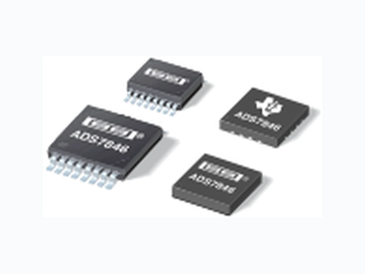
ADS7846NG4 BURR-BROWN
Document overview
- Manufacturer or author: Provided By digicamel.com
- PDF pages: 30
Technical content
FEATURES
G 2.2V TO 5.25V OPERATION G INTERNAL 2.5V REFERENCE G DIRECT BATTERY MEASUREMENT (0V to 6V) G ON-CHIP TEMPERATURE MEASUREMENT G TOUCH-PRESSURE MEASUREMENT G QSPI TM /SPITM 3-WIRE INTERFACE G AUTO POWER-DOWN G TSSOP-16, SSOP-16, QFN-16, AND VFBGA-48 PACKAGES
APPLICATIONS
G PERSONAL DIGITAL ASSISTANTS G PORTABLE INSTRUMENTS G POINT-OF-SALE TERMINALS G PAGERS G TOUCH SCREEN MONITORS G CELLULAR PHONES TOUCH SCREEN CONTROLLER
DESCRIPTION
The ADS7846 is a next-generation version to the industry standard ADS7843 4-wire touch screen controller. The ADS7846 is 100% pin-compatible with the existing ADS7843, and drops into the same socket. This allows for easy upgrade of current applications to the new version. Only software changes are required to take advantage of the added fea- tures of direct battery measurement, temperature measure- ment, and touch-pressure measurement. The ADS7846 also has an on-chip 2.5V reference that can be used for the auxiliary input, battery monitor, and temperature measure- ment modes. The reference can also be powered down when not used to conserve power. The internal reference operates down to 2.7V supply voltage while monitoring the battery voltage from 0V to 6V. The low-power consumption of < 0.75mW (typ at 2.7V, reference off), high speed (up to 125kHz clock rate), and on- chip drivers make the ADS7846 an ideal choice for battery- operated systems such as personal digital assistants (PDAs) with resistive touch screens, pagers, cellular phones, and other portable equipment. The ADS7846 is available in the small TSSOP-16, SSOP-16, QFN-16, and VFBGA-48 pack- ages and is specified over the –40°C to +85°C temperature range. CDAC Internal 2.5V Reference SAR ADS7846 Comparator 6-Channel MUX Serial Data Out Temperature Sensor Battery Monitor DOUT BUSY CS DCLK DIN VBAT AUX VREF +VCC PENIRQ ADS7846 SBAS125H – SEPTEMBER 1999 – REVISED JANUARY 2005 www.ti.com PRODUCTION DATA information is current as of publication date. Products conform to specifications per the terms of Texas Instruments standard warranty. Production processing does not necessarily include testing of all parameters. Copyright © 1999-2005, Texas Instruments Incorporated US Patent No. 6246394 QSPI and SPI are registered trademarks of Motorola. ®ADS7846 ADS7846 ADS7846 Please be aware that an important notice concerning availability, standard warranty, and use in critical applications of Texas Instruments semiconductor products and disclaimers thereto appears at the end of this data sheet. All trademarks are the property of their respective owners.
SBAS125Hwww.ti.com ABSOLUTE MAXIMUM RATINGS (1) NOTE: (1) Stresses above these ratings can cause permanent damage. Exposure to absolute maximum conditions for extended periods may degrade device reliability. MAXIMUM INTEGRAL SPECIFIED LINEARITY PACKAGE TEMPERATURE PACKAGE ORDERING PRODUCT ERROR (LSB) PACKAGE-LEAD DESIGNATOR RANGE MARKING NUMBER ADS7846E ±2 SSOP-16 DBQ –40°C to +85°C ADS7846E ADS7846E ADS7846N ±2 TSSOP-16 PW –40°C to +85°C ADS7846N ADS7846N ADS7846I ±2 VFBGA-48 GQC –40°C to +85°C ADS7846 ADS7846IGQCR ADS7846I ±2 QFN-16 RGV –40°C to +85°C ADS7846 ADS7846IRGVT NOTE: (1) For the most current package and ordering information, see the Package Option Addendum located at the end of this data sheet, or see the TI web site at www.ti.com. PACKAGE/ORDERING INFORMATION (1) ELECTROSTATIC DISCHARGE SENSITIVITY This integrated circuit can be damaged by ESD. Texas Instru- ments recommends that all integrated circuits be handled with appropriate precautions. Failure to observe proper handling and installation procedures can cause damage. ESD damage can range from subtle performance degradation to complete device failure. Precision integrated circuits may be more susceptible to damage because very small parametric changes could cause the device not to meet its published specifications.
SBAS125H www.ti.com ANALOG INPUT Full-Scale Input Span Positive Input-Negative Input 0 V REF V Absolute Input Range Positive Input –0.2 +V CC + 0.2 V Negative Input –0.2 +0.2 V Capacitance 25 pF Leakage Current 0.1 µA SYSTEM PERFORMANCE Resolution 12 Bits No Missing Codes 11 Bits Integral Linearity Error ±2 LSB (1) Offset Error ±6L S B Gain Error External V REF ±4L S B Noise Including Internal V REF 70 µVrms Power-Supply Rejection 70 dB SAMPLING DYNAMICS Conversion Time 12 CLK Cycles Acquisition Time 3 CLK Cycles Throughput Rate 125 kHz Multiplexer Settling Time 500 ns Aperture Delay 30 ns Aperture Jitter 100 ps Channel-to-Channel Isolation V IN = 2.5Vp-p at 50kHz 100 dB SWITCH DRIVERS On-Resistance Y+, X+ 5 Ω Y–, X– 6 Ω Drive Current(2) Duration 100ms 50 mA REFERENCE OUTPUT Internal Reference Voltage 2.45 2.50 2.55 V Internal Reference Drift 15 ppm/ °C Quiescent Current 500 µA REFERENCE INPUT Range 1.0 +V CC V Input Impedance SER/DFR = 0, PD1 = 0, 1 G Ω Internal Reference Off Internal Reference On 250 Ω BATTERY MONITOR Input Voltage Range 0.5 6.0 V Input Impedance Sampling Battery 10 k Ω Battery Monitor Off 1G Ω Accuracy External V REF = 2.5V –2+ 2 % Internal Reference –3+ 3 % TEMPERATURE MEASUREMENT Temperature Range –40 +85 °C Resolution Differential Method (3) 1.6 °C TEMP0 (4) 0.3 °C Accuracy Differential Method (3) ±2 °C TEMP0 (4) ±3 °C DIGITAL INPUT/OUTPUT Logic Family CMOS Logic Levels, Except PENIRQ VIH | IIH | ≤ +5µA+ V CC • 0.7 +V CC + 0.3 VIL | IIL | ≤ +5µA –0.3 +0.8 V VOH IOH = –250µA+ V CC • 0.8 V VOL IOL = 250µA 0.4 V PENIRQ VOL TA = 0°C to +85°C, 50kΩ Pull-Up 0.8 V Data Format Straight Binary POWER-SUPPLY REQUIREMENTS +V CC (5) Specified Performance 2.7 3.6 V Operating Range 2.2 5.25 V Quiescent Current Internal Reference Off 280 650 µA Internal Reference On 780 µA fSAMPLE = 12.5kHz 220 µA Power-Down Mode with 3 µA CS = DCLK = DIN = +VCC Power Dissipation +V CC = +2.7V 1.8 mW TEMPERATURE RANGE Specified Performance –40 +85 °C NOTES: (1) LSB means least significant bit. With VREF equal to +2.5V, one LSB is 610µV. (2) Ensured by design, but not tested. Exceeding 50mA source current (5) ADS7846 operates down to 2.2V. ADS7846E PARAMETER CONDITIONS MIN TYP MAX UNITS
ELECTRICAL CHARACTERISTICS
At TA = –40°C to +85°C, +VCC = +2.7V, VREF = 2.5V internal voltage, fSAMPLE = 125kHz, fCLK = 16 • fSAMPLE = 2MHz, 12-bit mode, and digital inputs = GND or +VCC , unless otherwise noted.
SBAS125Hwww.ti.com PIN CONFIGURATION Top View SSOP, TSSOP Top View VFBGA CC GND VBAT AUX DCLK CS DIN BUSY DOUT PENIRQ CC VREF ADS7846 NC NCA 21 3 4 5 6 7 DCLK +VCC +VCC PENIRQ +VCC VREF AUX CS DIN BUSY DOUT X– Y– GND GND V BAT NC NC NC NC NC B C D E F NC NC NC NC NC NC NC NC NC NC NC NC NC NC NC NC NC NC NC NC NCNC NCG BUSY DIN CS DCLK AUX VBAT GND ADS7846 DOUT PENIRQ CC VREF +VCC Top View QFN SSOP AND TSSOP PIN # VFBGA PIN # QFN PIN # NAME DESCRIPTION
1 B1 and C1 5 +V CC Power Supply
2 D1 6 X+ X+ Position Input
3 E1 7 Y+ Y+ Position Input
4G 28X – X– Position Input 5G 39Y – Y– Position Input
6 G4 and G5 10 GND Ground
8 E7 12 AUX Auxiliary Input to ADC
REF Voltage Reference Input/Output
10 C7 14 +V CC Digital I/O Power Supply
11 B7 15 PENIRQ Pen Interrupt. Open anode output (requires 10kΩ to 100kΩ pull-up resistor externally). 12 A6 16 DOUT Serial Data Output. Data is shifted on the falling edge of DCLK. This output is high impedance when CS is high. 13 A5 1 BUSY Busy Output. This output is high impedance when CS is high. 14 A4 2 DIN Serial Data Input. If CS is low, data is latched on rising edge of DCLK. 15 A3 3 CS Chip Select Input. Controls conversion timing and enables the serial input/output register. CS high = power-down mode (ADC only). 16 A2 4 DCLK External Clock Input. This clock runs the SAR conversion process and synchronizes serial data I/O. PIN DESCRIPTION
SBAS125H www.ti.com TYPICAL CHARACTERISTICS At TA = +25°C, +VCC = +2.7V, VREF = External +2.5V, fSAMPLE = 125kHz, and fCLK = 16 • fSAMPLE = 2MHz, unless otherwise noted. SUPPLY CURRENT vs TEMPERATURE 20–40 100–20 0 40 Temperature (°C) Supply Current (µA) 400 350 300 250 200 150 100 60 80 POWER-DOWN SUPPLY CURRENT vs TEMPERATURE 20–40 100–20 0 40 Temperature (°C) Supply Current (nA) 140 120 100 60 80 SUPPLY CURRENT vs +V CC +VCC (V) Supply Current (µA) 390 370 350 330 310 290 270 250 4.53.0 fSAMPLE = 12.5kHz MAXIMUM SAMPLE RATE vs +V CC +VCC (V) Sample Rate (Hz) 100k 10k 4.53.0 CHANGE IN GAIN vs TEMPERATURE 20–40 100–20 0 40 Temperature (°C) Delta from +25°C (LSB) 0.15 0.10 0.05 –0.05 –0.10 –0.15 60 80 CHANGE IN OFFSET vs TEMPERATURE 20–40 100–20 0 40 Temperature (°C) Delta from +25°C (LSB) 0.6 0.4 0.2 –0.2 –0.4 –0.6 60 80
SBAS125Hwww.ti.com TYPICAL CHARACTERISTICS (Cont.) At TA = +25°C, +VCC = +2.7V, VREF = External +2.5V, fSAMPLE = 125kHz, and fCLK = 16 • fSAMPLE = 2MHz, unless otherwise noted. REFERENCE CURRENT vs SAMPLE RATE 750 125 25 50 100 Sample Rate (kHz) Reference Current (µA) REFERENCE CURRENT vs TEMPERATURE 20–40 100–20 0 40 Temperature (°C) Reference Current (µA) 60 80 SWITCH-ON RESISTANCE vs TEMPERATURE (X+, Y+: +VCC to Pin; X–, Y–: Pin to GND) 20–40 100–20 X+ Y+ Y–X– Temperature (°C) R ON (Ω ) 60 800 2.4920 2.4915 2.4910 2.4905 2.4900 2.4895 2.4890 2.4885 2.4880 2.4875 Internal VREF (V) Temperature (°C) INTERNAL V REF vs TEMPERATURE –40 –35 –30 –25 –20 –15 –10 –05 SWITCH-ON RESISTANCE vs +V CC (X+, Y+: +VCC to Pin; X–, Y–: Pin to GND) 3.52.0 5.0 2.5 X+Y+ 4.0 +V CC (V) R ON (Ω ) 4.53.0 2.0 1.8 1.6 1.4 1.2 1.0 0.8 0.6 0.4 0.2 Error (LSB) 20 40 60 80 100 120 140 160 180 200 Sampling Rate (kHz) MAXIMUM SAMPLING RATE vs R IN INL: R = 2k INL: R = 500 DNL: R = 2k DNL: R = 500
SBAS125H www.ti.com TYPICAL CHARACTERISTICS (Cont.) At TA = +25°C, +VCC = +2.7V, VREF = External +2.5V, fSAMPLE = 125kHz, and fCLK = 16 • fSAMPLE = 2MHz, unless otherwise noted. 2.4865 2.4860 2.4855 2.4850 2.4845 2.4840 VREF (V) 2.5 2.6 2.7 2.8 2.9 3.0 3.1 3.2 3.3 3.4 3.5 3.6 VCC (V) INTERNAL V REF vs VCC 850 800 750 700 650 600 550 500 450 TEMP Diode Voltage (mV) Temperature (°C) –40 –35 –30 –25 –20 –15 –10 –05 TEMP DIODE VOLTAGE vs TEMPERATURE (2.7V SUPPLY) 102.7mV 132.25mV TEMP0 TEMP1 100 Internal VREF (%) 0 200 400 600 800 1000 1200 INTERNAL V REF vs TURN-ON TIME Turn-On Time (µS) 1µF Cap (1110µS) 12-Bit Settling No Cap (52µS) 12-Bit Settling 620 618 616 614 612 610 2.7 3.0 3.3 V SUPPLY (V) TEMP0 DIODE VOLTAGE vs V SUPPLY (25°C) TEMP0 Diode Voltage (mV) 732 730 728 726 724 722 2.7 3.0 3.3 V SUPPLY (V) TEMP1 DIODE VOLTAGE vs V SUPPLY (25°C) TEMP1 Diode Voltage (mV)
The basic operation of the ADS7846 is shown in Figure 1. input range of the converter. Digital Interface section of this data sheet for more details. to the converter is a function of conversion rate. FIGURE 1. Basic Operation of the ADS7846. TABLE I. Input Configuration (DIN), Single-Ended Reference Mode (SER/DFR high). TABLE II. Input Configuration (DIN), Differential Reference Mode (SER/DFR low).
SBAS125H www.ti.com sample-and-hold goes into the hold mode and the touch panel drivers turn off (in single-ended mode). The next 12 clock cycles accomplish the actual analog-to-digital conver- sion. If the conversion is ratiometric ( SER/DFR = 0), the drivers are on during the conversion and a 13th clock cycle is needed for the last bit of the conversion result. Three more clock cycles are needed to complete the last byte (DOUT will be low), which are ignored by the converter. Control Byte The control byte (on DIN), as shown in Table III, provides the start conversion, addressing, ADC resolution, configuration, and power-down of the ADS7846. Figure 9 and Tables III and IV give detailed information regarding the order and description of these control bits within the control byte. SER/DFR — The SER/DFR bit controls the reference mode, either single-ended (high) or differential (low). The differential mode is also referred to as the ratiometric conversion mode and is preferred for X-Position, Y-Position, and Pressure- Touch measurements for optimum performance. The refer- ence is derived from the voltage at the switch drivers, which is almost the same as the voltage to the touch screen. In this case a reference voltage is not needed, as the reference voltage to the ADC is the voltage across the touch screen. In the single-ended mode, the converter reference voltage is always the difference between the V REF and GND pins (see Tables I and II, and Figures 2 through 5 for further informa- tion). If X-Position, Y-Position, and Pressure-Touch are measured in the single-ended mode, an external reference voltage is needed. The ADS7846 should also be powered from the external reference. Caution must be observed when using the single-ended mode such that the input voltage to the ADC does not exceed the internal reference voltage, espe- cially if the supply voltage is greater than 2.7V. NOTE: The differential mode can only be used for X-Position, Y-Position, and Pressure-Touch measurements. All other measurements require the single-ended mode. PD0 and PD1 — Table V describes the power-down and the internal reference voltage configurations. The internal refer- ence voltage can be turned on or off independently of the ADC. This can allow extra time for the internal reference voltage to settle to the final value prior to making a conver- sion. Make sure to also allow this extra wake-up time if the internal reference is powered down. The ADC requires no wake-up time and can be instantaneously used. Also note that the status of the internal reference power-down is latched into the part (internally) with BUSY going high. Therefore, in order to turn the reference off, an additional write to the ADS7846 is required after the channel is con- verted. Bit 7 Bit 0 (MSB) Bit 6 Bit 5 Bit 4 Bit 3 Bit 2 Bit 1 (LSB) S A2 A1 A0 MODE SER/DFR PD1 PD0 TABLE III. Order of the Control Bits in the Control Byte. BIT NAME DESCRIPTION 7 S Start Bit. Control byte starts with first high bit on DIN. A new control byte can start every 15th clock cycle in 12-bit conversion mode or every 11th clock cycle in 8-bit conversion mode (see Figure 12). 6-4 A2-A0 Channel Select Bits. Along with the SER/DFR bit, these bits control the setting of the multiplexer input, touch driver switches, and reference inputs (see Tables I and II). 3 MODE 12-Bit/8-Bit Conversion Select Bit. This bit controls the number of bits for the next conversion: 12-bits (low) or 8-bits (high). SER/DFR Single-Ended/Differential Reference Select Bit. Along with bits A2-A0, this bit controls the setting of the multiplexer input, touch driver switches, and reference inputs (see Tables I and I). 1-0 PD1-PD0 Power-Down Mode Select Bits. See Table V for details. TABLE IV. Descriptions of the Control Bits within the Control Byte. Initiate START— The first bit, the S bit, must always be high and initiates the start of the control byte. The ADS7846 ignores inputs on the DIN pin until the start bit is detected. Addressing— The next three bits (A2, A1, and A0) select the active input channel(s) of the input multiplexer (see Tables I, II, and Figure 2), touch screen drivers, and the reference inputs. MODE — The mode bit sets the resolution of the ADC. With this bit low, the next conversion has 12 bits of resolution; with this bit high, the next conversion has 8 bits of resolution. PD1 PD0 PENIRQ DESCRIPTION 0 0 Enabled Power-Down Between Conversions. When each conversion is finished, the converter enters a low-power mode. At the start of the next conver- sion, the device instantly powers up to full power. There is no need for additional delays to assure full operation and the very first conversion is valid. The Y– switch is on when in power-down. 0 1 Disabled Reference is off and ADC is on. 1 0 Enabled Reference is on and ADC is off. 1 1 Disabled Device is always powered. Reference is on and ADC is on. TABLE V. Power-Down and Internal Reference Selection.
16 Clocks-per-Conversion
tween each byte transfer from the processor to the converter. digital interface of the ADS7846. FIGURE 11. Detailed Timing Diagram. FIGURE 10. Conversion Timing, 16 Clocks-per-Conversion, 8-Bit Bus Interface. No DCLK delay required with dedicated
15 Clocks-per-Conversion
Figure 12 provides the fastest way to clock the ADS7846. clock cycles per conversion. ADS7846 spends most of the time acquiring or converting. between the two modes is dramatic. FIGURE 12. Maximum Conversion Rate, 15 Clocks-per-Conversion. FIGURE 13. Ideal Input Voltages and Output Codes. NOTES: (1) Reference voltage at converter: +REF – (–REF), see Figure 2. (2) Input voltage at converter, after multiplexer: +IN – (–IN), see Figure 2.
FIGURE 15. ADS7846 PENIRQ Functional Block Diagram. error, much like the on-resistance of the internal switches. the contact resistance changes with flexing or vibrations. from Y+, Y–, X+, and X– pins to ground can also help. single-ended mode and at high data rates. screen to ground, which initiates an interrupt to the processor. X+ input is disconnected from the external pull-up resistor. cases discussed in this section.
www.ti.com 11-Apr-2013 Addendum-Page 1 PACKAGING INFORMATION Orderable Device Status (1) Package Type Package Drawing Pins Package Qty Eco Plan (2) Lead/Ball Finish MSL Peak Temp (3) Op Temp (°C) Top-Side Markings (4) Samples ADS7846E ACTIVE SSOP DBQ 16 75 Green (RoHS & no Sb/Br) CU NIPDAU Level-2-260C-1 YEAR -40 to 85 ADS 7846E ADS7846E/2K5 ACTIVE SSOP DBQ 16 2500 Green (RoHS & no Sb/Br) CU NIPDAU Level-2-260C-1 YEAR -40 to 85 ADS 7846E ADS7846E/2K5G4 ACTIVE SSOP DBQ 16 2500 Green (RoHS & no Sb/Br) CU NIPDAU Level-2-260C-1 YEAR -40 to 85 ADS 7846E ADS7846EG4 ACTIVE SSOP DBQ 16 75 Green (RoHS & no Sb/Br) CU NIPDAU Level-2-260C-1 YEAR -40 to 85 ADS 7846E ADS7846IGQCR OBSOLETE BGA MICROSTAR JUNIOR GQC 48 TBD Call TI Call TI -40 to 85 AZ7846 ADS7846IRGVR ACTIVE VQFN RGV 16 2500 Green (RoHS & no Sb/Br) CU NIPDAU Level-2-260C-1 YEAR -40 to 85 ADS 7846 ADS7846IRGVRG4 ACTIVE VQFN RGV 16 2500 Green (RoHS & no Sb/Br) CU NIPDAU Level-2-260C-1 YEAR -40 to 85 ADS 7846 ADS7846IRGVT ACTIVE VQFN RGV 16 250 Green (RoHS & no Sb/Br) CU NIPDAU Level-2-260C-1 YEAR -40 to 85 ADS 7846 ADS7846IRGVTG4 ACTIVE VQFN RGV 16 250 Green (RoHS & no Sb/Br) CU NIPDAU Level-2-260C-1 YEAR -40 to 85 ADS 7846 ADS7846N ACTIVE TSSOP PW 16 90 Green (RoHS & no Sb/Br) CU NIPDAU Level-2-260C-1 YEAR -40 to 85 ADS 7846N ADS7846N/2K5 ACTIVE TSSOP PW 16 2500 Green (RoHS & no Sb/Br) CU NIPDAU Level-2-260C-1 YEAR -40 to 85 ADS 7846N ADS7846N/2K5G4 ACTIVE TSSOP PW 16 2500 Green (RoHS & no Sb/Br) CU NIPDAU Level-2-260C-1 YEAR -40 to 85 ADS 7846N ADS7846NG4 ACTIVE TSSOP PW 16 90 Green (RoHS & no Sb/Br) CU NIPDAU Level-2-260C-1 YEAR -40 to 85 ADS 7846N (1) The marketing status values are defined as follows: ACTIVE: Product device recommended for new designs. LIFEBUY: TI has announced that the device will be discontinued, and a lifetime-buy period is in effect. NRND: Not recommended for new designs. Device is in production to support existing customers, but TI does not recommend using this part in a new design. PREVIEW: Device has been announced but is not in production. Samples may or may not be available. OBSOLETE: TI has discontinued the production of the device.
www.ti.com 11-Apr-2013 Addendum-Page 2 (2) Eco Plan - The planned eco-friendly classification: Pb-Free (RoHS), Pb-Free (RoHS Exempt), or Green (RoHS & no Sb/Br) - please check http://www.ti.com/productcontent for the latest availability information and additional product content details. TBD: The Pb-Free/Green conversion plan has not been defined. Pb-Free (RoHS): TI's terms "Lead-Free" or "Pb-Free" mean semiconductor products that are compatible with the current RoHS requirements for all 6 substances, including the requirement that lead not exceed 0.1% by weight in homogeneous materials. Where designed to be soldered at high temperatures, TI Pb-Free products are suitable for use in specified lead-free processes. Pb-Free (RoHS Exempt): This component has a RoHS exemption for either 1) lead-based flip-chip solder bumps used between the die and package, or 2) lead-based die adhesive used between the die and leadframe. The component is otherwise considered Pb-Free (RoHS compatible) as defined above. Green (RoHS & no Sb/Br): TI defines "Green" to mean Pb-Free (RoHS compatible), and free of Bromine (Br) and Antimony (Sb) based flame retardants (Br or Sb do not exceed 0.1% by weight in homogeneous material) (3) MSL, Peak Temp. -- The Moisture Sensitivity Level rating according to the JEDEC industry standard classifications, and peak solder temperature. (4) Multiple Top-Side Markings will be inside parentheses. Only one Top-Side Marking contained in parentheses and separated by a "~" will appear on a device. If a line is indented then it is a continuation of the previous line and the two combined represent the entire Top-Side Marking for that device. Important Information and Disclaimer:The information provided on this page represents TI's knowledge and belief as of the date that it is provided. TI bases its knowledge and belief on information provided by third parties, and makes no representation or warranty as to the accuracy of such information. Efforts are underway to better integrate information from third parties. TI has taken and continues to take reasonable steps to provide representative and accurate information but may not have conducted destructive testing or chemical analysis on incoming materials and chemicals. TI and TI suppliers consider certain information to be proprietary, and thus CAS numbers and other limited information may not be available for release. In no event shall TI's liability arising out of such information exceed the total purchase price of the TI part(s) at issue in this document sold by TI to Customer on an annual basis.
*All dimensions are nominal Device Package Type Package Drawing Pins SPQ Reel Diameter (mm) Reel Width W1 (mm) (mm) (mm) (mm) (mm) W (mm) Pin1 Quadrant PACKAGE MATERIALS INFORMATION www.ti.com 24-Apr-2013 Pack Materials-Page 1
*All dimensions are nominal Device Package Type Package Drawing Pins SPQ Length (mm) Width (mm) Height (mm) ADS7846E/2K5 SSOP DBQ 16 2500 367.0 367.0 35.0 ADS7846IRGVR VQFN RGV 16 2500 338.1 338.1 20.6 ADS7846IRGVT VQFN RGV 16 250 210.0 185.0 35.0 PACKAGE MATERIALS INFORMATION www.ti.com 24-Apr-2013 Pack Materials-Page 2
MPLG008D – APRIL 2000 – REVISED FEBRUARY 2002 1POST OFFICE BOX 655303 • DALLAS, TEXAS 75265 GQC (S-PBGA-N48) PLASTIC BALL GRID ARRAY 0,50 M0,05 0,50 0,08 4200460/E 01/02 4,10 3,90 1,00 MAX 0,25 0,35 A Seating Plane 3,00 TYP B C D E F 2 3 4 5 6 7 G 0,77 SQ 0,25 0,15 A1 Corner Bottom View 3,00 TYP 0,71 NOTES: A. All linear dimensions are in millimeters. B. This drawing is subject to change without notice. C. MicroStar Junior BGA configuration D. Falls within JEDEC MO-225 MicroStar Junior is a trademark of Texas Instruments.
Texas InstrumentsIncorporatedand itssubsidiaries(TI)reservetherighttomake corrections,enhancements,improvementsand other changes toitssemiconductorproductsand servicesperJESD46, latestissue,and todiscontinueany productorserviceperJESD48, latest issue.Buyersshouldobtainthelatestrelevantinformationbeforeplacingordersand shouldverifythatsuch informationiscurrentand complete.Allsemiconductorproducts(alsoreferredtohereinas “components”)aresoldsubjecttoTI’s termsand conditionsofsale suppliedatthetimeoforderacknowledgment. TIwarrantsperformanceofitscomponents tothespecificationsapplicableatthetimeofsale,inaccordancewiththewarrantyinTI’s terms and conditionsofsaleofsemiconductorproducts.Testingand otherqualitycontroltechniquesareused totheextentTIdeems necessary tosupportthiswarranty.Exceptwhere mandated by applicablelaw,testingofallparametersofeach component isnotnecessarily performed. TIassumes no liabilityforapplicationsassistanceorthedesignofBuyers’products.Buyersareresponsiblefortheirproductsand applicationsusingTIcomponents.To minimizetherisksassociatedwithBuyers’productsand applications,Buyersshouldprovide adequatedesignand operatingsafeguards. TIdoes notwarrantorrepresentthatany license,eitherexpressorimplied,isgrantedunderany patentright,copyright,mask work right,or otherintellectualpropertyrightrelatingtoany combination,machine,orprocessinwhichTIcomponents orservicesareused.Information publishedby TIregardingthird-partyproductsorservicesdoes notconstitutea licensetouse such productsorservicesora warrantyor endorsementthereof.Use ofsuch informationmay requirea licensefroma thirdpartyunderthepatentsorotherintellectualpropertyofthe thirdparty,ora licensefromTIunderthepatentsorotherintellectualpropertyofTI. ReproductionofsignificantportionsofTIinformationinTIdatabooks ordatasheetsispermissibleonlyifreproductioniswithoutalteration and isaccompaniedby allassociatedwarranties,conditions,limitations,and notices.TIisnotresponsibleorliableforsuch altered documentation.Informationofthirdpartiesmay be subjecttoadditionalrestrictions. ResaleofTIcomponents orserviceswithstatementsdifferentfromorbeyond theparametersstatedby TIforthatcomponent orservice voidsallexpressand any impliedwarrantiesfortheassociatedTIcomponent orserviceand isan unfairand deceptivebusinesspractice. TIisnotresponsibleorliableforany such statements. Buyeracknowledgesand agreesthatitissolelyresponsibleforcompliancewithalllegal,regulatoryand safety-relatedrequirements concerningitsproducts,and any use ofTIcomponents initsapplications,notwithstandingany applications-relatedinformationorsupport thatmay be providedby TI.Buyerrepresentsand agreesthatithas allthenecessaryexpertisetocreateand implementsafeguardswhich anticipatedangerousconsequencesoffailures,monitorfailuresand theirconsequences,lessenthelikelihoodoffailuresthatmightcause harm and takeappropriateremedialactions.BuyerwillfullyindemnifyTIand itsrepresentativesagainstany damages arisingoutoftheuse ofany TIcomponents insafety-criticalapplications. Insome cases,TIcomponents may be promotedspecificallytofacilitatesafety-relatedapplications.Withsuch components,TI’s goalisto helpenablecustomerstodesignand createtheirown end-productsolutionsthatmeet applicablefunctionalsafetystandardsand requirements.Nonetheless,such components aresubjecttotheseterms. No TIcomponents areauthorizedforuse inFDA ClassIII(orsimilarlife-criticalmedicalequipment)unlessauthorizedofficersoftheparties have executeda specialagreementspecificallygoverningsuch use. OnlythoseTIcomponents whichTIhas specificallydesignatedas militarygradeor“enhanced plastic”aredesignedand intendedforuse in military/aerospaceapplicationsorenvironments.Buyeracknowledgesand agreesthatany militaryoraerospaceuse ofTIcomponents whichhave not been so designatedissolelyattheBuyer's risk,and thatBuyerissolelyresponsibleforcompliancewithalllegaland regulatoryrequirementsinconnectionwithsuch use. TIhas specificallydesignatedcertaincomponents as meetingISO/TS16949 requirements,mainlyforautomotiveuse.Inany case ofuse of non-designatedproducts,TIwillnotbe responsibleforany failuretomeet ISO/TS16949. Products Applications Audio www.ti.com/audio Automotiveand Transportationwww.ti.com/automotive Amplifiers amplifier.ti.com Communicationsand Telecom www.ti.com/communications Data Converters dataconverter.ti.com Computers and Peripherals www.ti.com/computers DLP ® Products www.dlp.com Consumer Electronics www.ti.com/consumer-apps DSP dsp.ti.com Energyand Lighting www.ti.com/energy Clocksand Timers www.ti.com/clocks Industrial www.ti.com/industrial Interface interface.ti.com Medical www.ti.com/medical Logic logic.ti.com Security www.ti.com/security Power Mgmt power.ti.com Space,Avionicsand Defense www.ti.com/space-avionics-defense Microcontrollers microcontroller.ti.com Videoand Imaging www.ti.com/video RFID www.ti-rfid.com OMAP ApplicationsProcessors www.ti.com/omap TIE2E Community e2e.ti.com WirelessConnectivity www.ti.com/wirelessconnectivity MailingAddress:Texas Instruments,PostOfficeBox 655303,Dallas,Texas 75265 Copyright© 2013,Texas InstrumentsIncorporated