
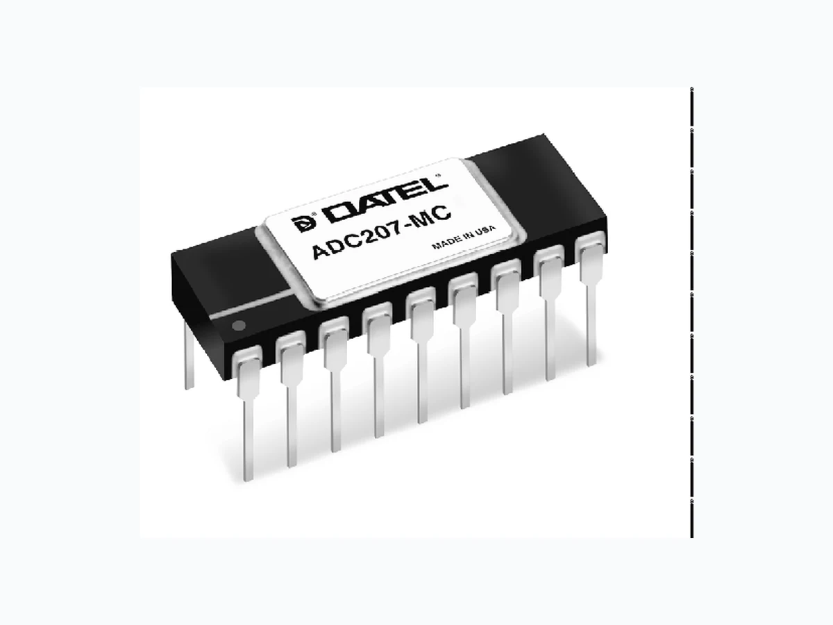
ADC-207 ETC
Document overview
- Manufacturer or author: Provided By www.digicamel.com(FREE DATASHEET DOWNLOAD SITE)
- PDF pages: 6
Technical content
INN O VAT IO N an d E X C ELL E N C E ® ® INPUT/OUTPUT CONNECTIONS DIP LCC PINS FUNCTION PINS
1 CLOCK INPUT 1
2 DIGITAL GROUND 4
3 –REFERENCE 5
4 ANALOG INPUT 6
5 MIDPOINT 7
7 ANALOG GROUND 9
8 CS1 11
9 CS2 12
10 OVERFLOW 13
11 BIT 1 (MSB) 14
12 BIT 2 16
13 BIT 3 17
14 BIT 4 19
15 BIT 5 20
16 BIT 6 21
17 BIT 7 (LSB) 23
Figure 1. ADC-207 Functional Block Diagram (DIP Pinout)
FEATURES
- 7-bit flash A/D converter
- 20MHz sampling rate
- Low power (250mW)
- Single +5V supply
- 1.2 micron CMOS technology
- 7-bit latched 3-state output with overflow bit
- Surface-mount versions
- High-reliability version
- No missing codes GENERAL DESCRIPTION The ADC-207 is the industry’s first 7-bit flash converter using an advanced high-speed VLSI 1.2 micron CMOS process. This process offers some very distinctive advantages over other processes, making the ADC-207 unique. The smaller geometrics of the process achieve high speed, better linearity and superior temperature performance. Since the ADC-207 is a CMOS device, it also has very low power consumption (250mW). The device draws power from a single +5V supply and is conservatively rated for 20MHz operation. The ADC-207 allows using sampling apertures as small as 12ns, making it more closely approach an ideal sampler. The small sampling apertures also let the device operate at greater than 20MHz. The ADC-207 has 128 comparators which are auto-balanced on every conversion to cancel out any offsets due to temperature and/or dynamic effects. The resistor ladder has a midpoint tap for use with an external voltage source to improve integral linearity beyond 7 bits. The ADC-207 also provides the user with 3-state outputs for easy interfacing to other components. There are six models of the ADC-207 covering two operating temperature ranges, 0 to +70°C and –55 to +125°C. Two high- reliability "QL" models are also available. D G Q D G Q D G Q D G Q D G Q D G Q D G Q D G Q D G Q D G Q D G Q D G Q D G Q D G Q ANALOG INPUT 4 +REFERENCE 6 DIGITAL GROUND 2 ANALOG GROUND 7 RANGE MIDPOINT 5 R/2 R R R R R/2 R/2 –REFERENCE 3 CS1 8 +5V SUPPLY 18 +VDD
1 CLOCK INPUTCLOCK
10 OVERFLOW
11 BIT 1 (MSB)
12 BIT 2
13 BIT 3
14 BIT 4
15 BIT 5
16 BIT 6
17 BIT 7 (LSB)
D G Q D G Q D G Q D G Q ∅ 1 ∅ 2 ∅ 2 ∅ 1 ADC-207 7-Bit, 20MHz, CMOS Flash A/D Converters DATEL, Inc., 11 Cabot Boulevard, Mansfield, MA 02048-1151 (U.S.A.) • Tel: (508) 339-3000 Fax: (508) 339-6356 • For immediate assistance (800) 233-2765
- Input Buffer Amplifier – Since the ADC-207 has a switched
- Reference Ladder – Adjusting the voltage at +REFERENCE
REFERENCE adjusts the offset or zero of the ADC-207.
- Clock Pulse Width – To improve performance at Nyquist
- At sampling rates less than 100kHz, there may be some
degradation in offset and differential nonlinearity. cycle (decreasing the time spent in the sample mode). Figure 2. Typical Connections for Using the ADC-207 ➀ At full power input and chip selects enabled. ➁ At 4MHz input and 20MHz clock. ➂ For 10-step, 40 IRE NTSC ramp test. ➃ Adjustable using reference ladder midpoint tap. See ADC-207 Operation.
the code transition to the proper midpoint values. Table 2. Chip Select Truth Table comparators are also connected to 128 sampling capacitors. switches. This forces the comparators to trip either high or low. transition point, they can trip very quickly to the correct state. an output latch. This latch then feeds the 3-state output buffer. followed by a negative pulse followed by a positive pulse. Table 1. ADC-207 Output Coding *Note that the overflow code does not clear the data bits.
circuit connections for the application. ADC-207’s high-frequency performance. array to determine spectral purity, harmonic distortion, etc.
- Full power input bandwidth of all 128 comparators.
- Phase response linearity vs. instantaneous signal
- Comparator slew rate limiting.
Figure 6 shows an actual ADC-207 plot of the Envelope Test. Figure 3. Optional Pulse Shaping Circuit Figure 4. Using Two ADC-207’s for 8-Bit Operation by a bit to the device B’s output.
11 CLOCK OUT
MECHANICAL DIMENSIONS INCHES (MM)
ORDERING INFORMATION
MODEL TEMP. RANGE PACKAGE ADC-207MC 0 to +70°C 18-pin DIP ADC-207MM –55 to +125°C 18-pin DIP ADC-207MM-QL –55 to +125°C 18-pin DIP ADC-207LC 0 to +70°C 24-pin CLCC ADC-207LM –55 to +125°C 24-pin CLCC ADC-207LM-QL –55 to +125°C 24-pin CLCC ACCESSORIES ADC-B207/208 Evaluation Board for DIP Version (without ADC-207) 0.400 (10.16 ) 0.250 ±0.005 (6.35 ±0.13) 0.050 (1.270) TYP. 0.020 ±0.005 (0.51 ±0.13) 0.090 MAX. (2.29 MAX.) +0.010 –0.005 +0.25 –0.13 0.400 (10.16 ) +0.010 –0.005 +0.25 –0.13 0.250 ±0.005 (6.35 ±0.13) PIN 1 INDEX TOP VIEW 24-Pin Ceramic LCC18-Pin Ceramic DIP 0.960 MAX. (24.38 MAX.) 0.220 / 0.310 (5.59 / 7.87) DATEL ADC-207MC PIN 1 IDENTIFIER 18 10 0.200 MAX. (5.1 MAX.) 0.100 TYP. (2.540) 0.014 / 0.023 (0.35 / 0.58) 0.015 / 0.060 (0.38 /1.52) 0.290 / 0.320 (7.36 / 8.13) SEATING PLANE 0.035 (0.889) 0.008 / 0.015 (0.20 / 0.38) IN N OVAT ION a nd E X C ELL E N C E ® ® DATEL makes no representation that the use of its products in the circuits described herein, or the use of other technical information contained herein, will not infringe upon existing or future patent rights. The descriptions contained herein do not imply the granting of licenses to make, use, or sell equipment constructed in accordance therewith. Specifications are subject to change without notice. The DATEL logo is a registered DATEL, Inc. trademark. DS-0038C 12/04 ISO 9001ISO 9001 REGISTERED ADC-207 ® ® DATEL, Inc. 11 Cabot Boulevard, Mansfield, MA 02048-1151 Tel: (508) 339-3000 (800) 233-2765 Fax: (508) 339-6356 Internet: www.datel.com E-mail:sales@datel.com Data Sheet Fax Back: (508) 261-2857 DATEL (UK) LTD. Tadley, England Tel: (01256)-880444 DATEL S.A.R.L. Montigny Le Bretonneux, France Tel: 1-34-60-01-01 DATEL GmbH München, Germany Tel: 89-544334-0 DATEL KK Tokyo, Japan Tel: 3-3779-1031, Osaka Tel: 6-354-2025