

 Download PDF
AD500-9-400M-TO5 SENSORTECHNICS
Document overview
- PDF pages: 3
Technical content
Page 1
First Sensor APD Hybrid Series Data Sheet
Part Description AD500-9-400M-TO5
US Order # 05-051-01, # 05-051-02
International Order # 50049001, # 50049002
FEATURES
DESCRIPTION
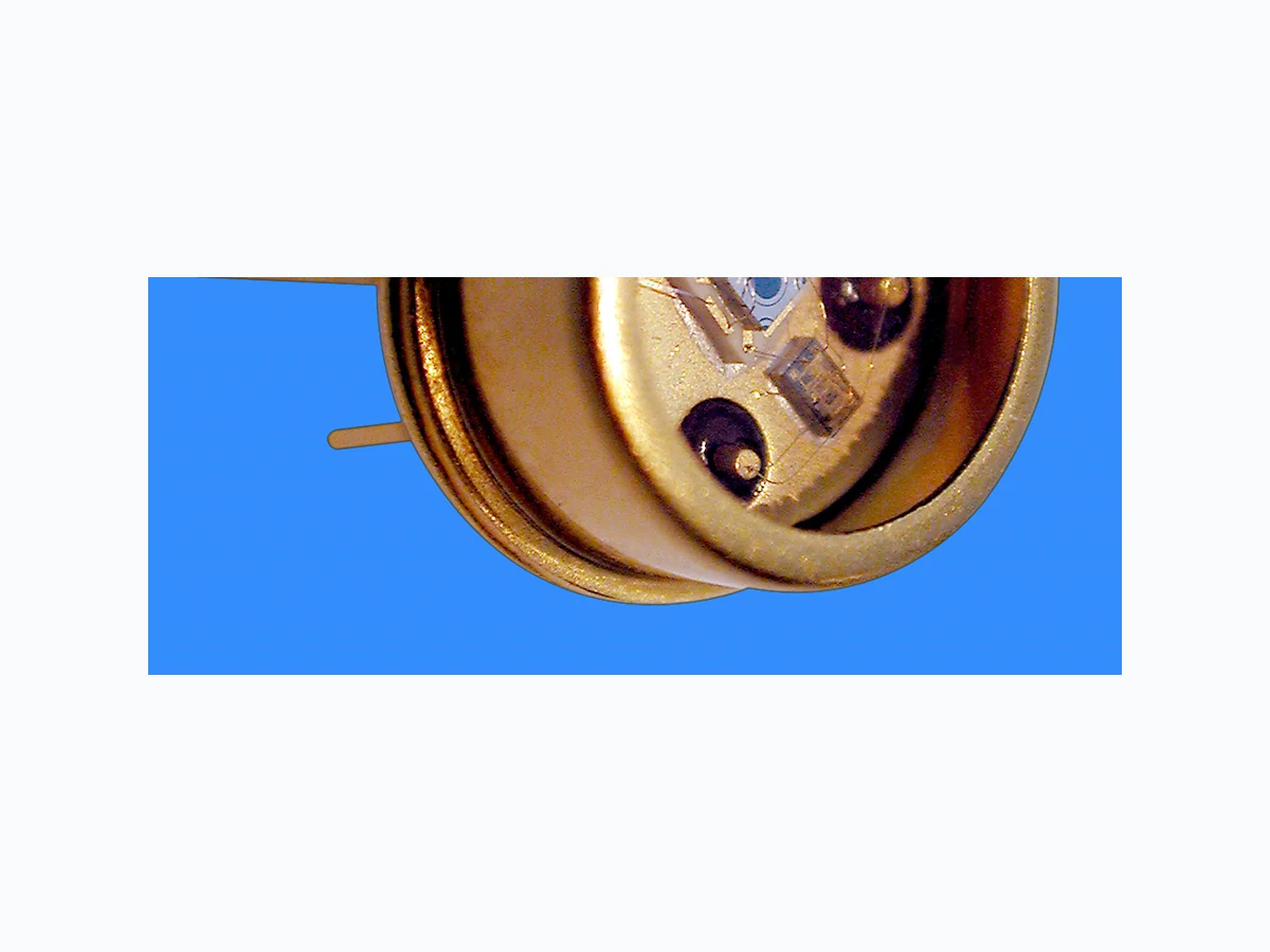
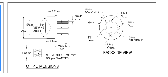
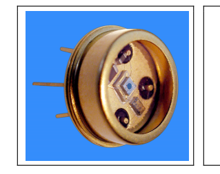
The AD500-9-400M-TO5 is an Avalanche Photodiode Amplifier
- ∅ 0.500 mm active area
Hybrid containing a 0.196 mm2 active area APD chip integrated
- Low noise
with an internal transimpedance amplifier. Hermetically
- High gain
packaged in a TO-5 with a borosilicate glass window cap.
- Long term stability
APPLICATIONS
- Lidar
- Analytical instruments
- Medical equipment
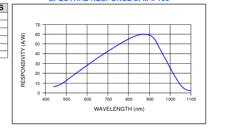
SPECTRAL RESPONSE at M = 100
ABSOLUTE MAXIMUM RATING
| SYMBOL | PARAMETER | MIN | MAX |
|---|---|---|---|
| T STG | Storage Temp | -55 | +125 |
| T OP | Operating Temp | 0 | +60 |
| T SOLDERING | Soldering Temp | - | +240 |
| P | Power Dissipation | - | 360 |
| V cc | Single Supply Voltage | +3.0 | +5.5 |
| I cc | Supply Current | - | 63 |
UNITS
°C °C °C mW V mA
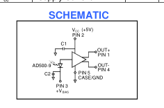
ELECTRO-OPTICAL CHARACTERISTICS @ 23°°°° C (VCC = single supply +3.3V, RL = 100W unless otherwise specified)
| SYMBOL | CHARACTERISTIC | TEST CONDITIONS MIN T | YP MAX UNITS |
|---|---|---|---|
| ƒ -3dB | Frequency Response | -3dB @ 905 nm --- 4 | 00 --- MHz |
| S | Sensitivity* | λ = 905 nm; M = 100 --- 1 | 45 --- mV/µW |
| I cc | Supply Current | Dark state --- 3 | 4 63 mA |
\* Sensitivity = APD responsivity (0.58 A/W X 100 gain) x TIA gain (2.5K)
Use US order number 05-051-01, or International order number 50049001 for breakdown voltage range of 160-200 Volts. Use US order number 05-051-02, or International order number 50049002 for breakdown voltage range of 200-240 Volts.
These devices are sensitive to electrostatic discharge. Please use ESD precautions when handling.
Disclaimer: Due to our policy of continued development, specifications are subject to change without notice.
Page 2
AVALANCHE PHOTODIODE DATA @ 23 °°°°C
| SYMBOL | CHARACTERISTIC | TEST CONDITIONS | MIN | TYP | MAX | UNITS |
|---|---|---|---|---|---|---|
| I D | Dark Current | M = 100 (see note 2) | --- | 0.8 | 5.0 | nA |
| C | Capacitance | M = 100 (see note 2) | --- | 1.2 | --- | pF |
| V BR | Breakdown Voltage (see note 1) | I = 2 µA D | 160 | --- | 240 | V |
| Temperature Coefficient of V BR | 1.25 | --- | 1.55 | V/K | ||
| Responsivity | M = 100;= 0 V; λ = 905 nm | 52 | 58 | 60 | A/W | |
| ∆ƒ 3dB | Bandwidth | -3dB | --- | 0.5 | --- | GHz |
| tr | Rise Time | M = 100 | --- | 0.55 | --- | ns |
| Optimum Gain | 50 | 60 | --- | |||
| “Excess Noise” factor | M = 100 | --- | 2.5 | --- | ||
| “Excess Noise” index | M = 100 | --- | 0.2 | --- | ||
| Noise Current | M = 100 | --- | 1.0 | --- | pA/Hz1/2 | |
| Max Gain | 200 | --- | --- | |||
| NEP | Noise Equivalent Power | M = 100; λ = 905 nm | --- | 2.0 X 10⁻¹⁴ | --- | W/Hz1/2 |
Note 1: The following different breakdown voltage ranges are available: (160 – 200 V), (200 – 240 V). Note 2: Measurement conditions: Setup of photo current 1 nA at M = 1 and irradiated by a 880 nm, 80 nm bandwidth LED. Increase the photo current up to 100 nA, (M = 100) by internal multiplication due to an increasing bias voltage.
TRANSIMPEDANCE AMPLIFIER DATA @ 25 °°°°C
(Vcc = +3.0 V to 5.5 V, TA = 0°C to 70°C, 100Ω load between OUT+ and OUT-. Typical values are at TA = 25°C, Vcc = +3.3 V)
| PARAMETER | TEST CONDITIONS | MIN | TYP | MAX | UNITS |
|---|---|---|---|---|---|
| Supply Voltage | 3 | 5 | 5.5 | V | |
| Supply Current | --- | 34 | 63 | mA | |
| Transimpedance | Differential, measured with 40 µA p-p signal | 2.10 | 2.75 | 3.40 | kΩ |
| Output impedance | Single ended per side | 48 | 50 | 52 | Ω |
| Maximum Differential Output Voltage | Input = 2 mA p-p with 100 Ω differential termination | 220 | 380 | 575 | mV p-p |
| AC Input Overload | 2 | --- | --- | mA p-p | |
| DC Input Overload | 1 | --- | --- | mA | |
| Input Referred RMS Noise | TO-5 package, see note 4 | --- | 490 | 668 | nA |
| Input Referred Noise Density | See note 4 | --- | 11 | --- | pA/Hz1/2 |
| Small signal bandwidth | Source capacitance = 0.85 pF, see note 3 | 1.525 | 2.00 | --- | GHz |
| Low Frequency Cutoff | -3 dB, input < 20 µA DC | --- | 30 | --- | kHz |
| Transimpedance Linear Range | Peak to peak 0.95 < linearity < 1.05 | 40 | --- | --- | µA p-p |
| Power Supply Rejection Ratio (PSRR) | Output referred, f < 2 MHz, PSSR = -20 Log (∆Vout / ∆Vcc) | --- | 50 | --- | dB |
Note 3: Source capacitance for AD500-9-400M-TO5 is the capacitance of APD. Note 4: Input referred noise is calculated as RMS output noise/ (gain at f = 10 Mhz). Noise density is (input referred noise)/√bandwidth.
TRANSFER CHARACTERISTICS
The circuit used is an avalanche photodiode directly coupled to a high speed data handling transimpedance amplifier. The output of the APD (light generated current) is applied to the input of the amplifier. The amplifier output is in the form of a differential voltage pulsed signal.
The APD responsivity curve is provided in Fig. 2. The term Amps/Watt involves the area of the APD and can be expressed as Amps/mm2/Watts/mm2, where the numerator applies to the current generated divided by the area of the detector, the denominator refers to the power of the radiant energy present per unit area. As an example assume a radiant input of 1 microwatt at 905 nm. The APD’s corresponding responsivity is 0.58 A/W.
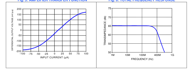
If energy in = 1 µW, then the current from the APD = (0.58 A/W) x (1x10⁻⁶W) = 0.58 µA. We can then factor in the typical gain of the APD of 100, making the input current to the amplifier 58 µA. From Fig. 5 we can see the amplifier output will be approximately 100 mV p-p.
APPLICATION NOTES
The AD500-9-400M-TO5 is a high speed optical data receiver. It incorporates an internal transimpedance amplifier with an avalanche photodiode.
This detector requires +3.5 V to +5.0 V voltage supply for the amplifier and a high voltage supply (100-240 V) for the APD. The internal APD follows the gain curve published for the AD500-9-TO52-S1 avalanche photodiode. The transimpedance amplifier provides differential output signals in the range of 200 millivolts differential.
In order to achieve highest gain, the avalanche photodiode needs a positive bias voltage (Fig. 1). However, a current limiting resistor must be placed in series with the photodiode bias voltage to limit the current into the transimpedance amplifier. Failure to limit this current may result in permanent failure of the device. The suggested initial value for this limiting resistor is 390 KOhm.
When using this receiver, good high frequency placement and routing techniques should be followed in order to achieve maximum frequency response. This includes the use of bypass capacitors, short leads and careful attention to impedance matching. The large gain bandwidth values of this device also demand that good shielding practices be used to avoid parasitic oscillations and reduce output noise.
Page 3
Fig. 1: APD GAIN vs BIAS VOLTAGE Fig. 2: APD SPECTRAL RESPONSE (M = 1)
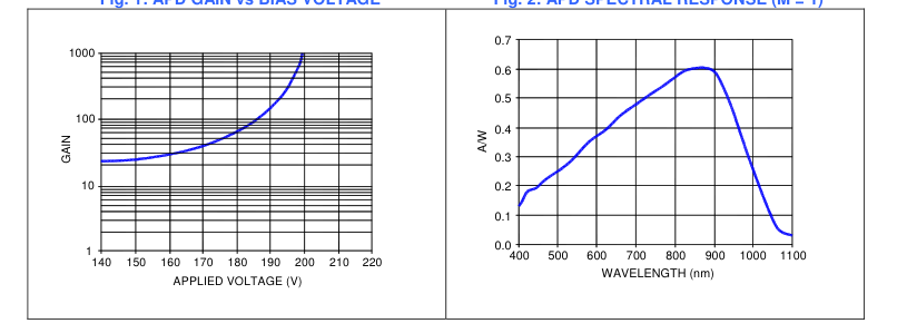
Fig. 3 : AMPLIFIER OUTPUT vs TEMPERATURE Fig.4 : APD CAPACITANCE vs BIAS VOLTAGE
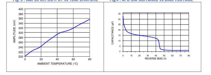
Fig. 5: AMPLIFIER TRANSFER FUNCTION Fig. 6: TOTAL FREQUENCY RESPONSE
USA: First Sensor, Inc. 5700 Corsa Avenue, #105 Westlake Village, CA 91362 USA T + 818 706-3400 F + 818 889-7053 contact.us@first-sensor.com www.first-sensor.com
International sales: First Sensor AG Peter-Behrens-Str. 15 12459 Berlin, Germany T + 49 30 6399 2399 F + 49 30 639923-752 sales.opto@first-sensor.com www.first-sensor.com