
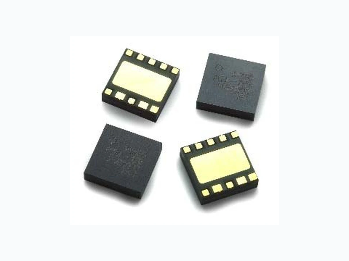
ACPM-7886 AVAGO
Document overview
- Manufacturer or author: Provided By www.digicamel.com(FREE DATASHEET DOWNLOAD SITE)
- PDF pages: 14
Technical content
Features
- Operating frequency: 2010 - 2025 MHz
- 28 dBm Linear Output Power @ 3.5V
- High Efficiency 41% PAE
- Single bias, low quiescent current (50mA)
- Internal 50 ohm matching networks for both RF input & output
- 3.2 - 4.2 V linear operation
- 4.0 x 4.0mm SMT Package
- Low package profile, 1.1mm
Applications
- TD-SCDMA Handsets
- TD-SCDMA Data Cards
- TD-SCDMA PDAs
Pin Number Pin Label Description Function 1 Vdd1 Supply bias 1 st and 2 nd stages drain bias, nominally 3.5V 2 RFin RF input Signal input, internally grounded through inductor. External DC block needed if DC voltage present on input trace.
3 N/C No internal connection Recommend ground connection on PCB
4 Vctrl Control voltage Output level control, nominally 2V
5 Vdd2 Supply bias Bias circuit supply, > 2.5V; nominally 2.85V. Does not require a regulated input and can be connected directly to the battery, if desired. 6G n d G r o u n d 7G n d G r o u n d
8 RFout RF output Signal output, requires external DC block
10 Vdd3 Supply bias 3 rd stage drain bias, nominally 3.5V AVAGO ACPM-7886 MLYWWDD XXXX Vdd1 (Pin 1) RFin N/C (GND) Vctrl Vdd2 (Pin 5) GND GND GND (Pin 6) RFout Vdd3 (Pin 10) 4mm sq 1.175mm Bottom View max
Notes: 1. Operation of this device in excess of any of these limits may cause permanent damage. 2. Avoid electrostatic discharge on I/O pins Parameter Min. Max. Supply voltage, Vdd1 and Vdd3 5.0 V Supply voltage, Vdd2 -1 V 5.0 V Analog control voltage -1 V 3.0 V RF input power +5 dBm Operating case temperature +90 °C Load VSWR 12:1 Storage temperature (case temperature) -30 °C +100 °C Recommended Operating Conditions Parameter Min. Typ. Max. Supply voltage, Vdd1 and Vdd3 1.0 V 3.5 V 4.5 V Supply voltage, Vdd2 2.6 V 2.85 V 4.5 V Control voltage 1.9 V 2.0 V 2.1 V Case temperature -20 °C +85 °C Package Dimensions Marking Notes : Row 3: ML = Manufacturing Location Y = Year WW = Work Week DD = Date Code Row 4: XXXX = Trace Code (Avago Technologies internal reference) 4.00 ± 0.075mm 4.00 ± 0.075mm 0.50mm0.40mm 0.45mm 0.10mm 0.10mm 2.00mm 0.50mm 0.60mm 0.40mm 0.60mm 3.80mm Viewed down through top of package Maximum Ratings Table
Electrical Characteristics of TD-SCDMA PA Unless Otherwise Specified: f=2010-2025MHz, Vdd1=Vdd3=3.5V, Vdd2=2.85V, Vctrl=2.0V, Pout=28.0dBm, Ta=25°C, Zin/Zout = 50 Ω PA Operation/Shutdown Logic: DC signals Parameter min typ Max Units Leakage Current, Idd1,2,3; Vctrl=0 V, RF Off 20 80 uA Control Current, Ictrl; Vctrl=2.0 V 75 110 145 uA Bias Current, Idd2; Vctrl=2 V, Vdd2=2.85 V 6 10 mA Quiescent Current, Idd1,3; RF Off Vctrl=2.0 V 50 80 mA At Pout=28.0dBm Supply current Idd1+Idd3 435 480 mA PAE including Vdd1,2,3 36 41 % Gain 25.5 28.5 32 dB Input VSWR 1.1 2.0:1 - ACLR 1.6MHz offset -40 -35 dBc/1.28MHz 3.2MHz offset -54 -48 dBc/1.28MHz 2nd Harmonic -50 -40 dBc/1MHz 3rd Harmonic -60 -45 dBc/1MHz Noise Figure 3.1 4.1 dB Stability, no spurious under conditions: VSWR=4:1, all phases 3<Vdd<4.5, -50 dBm to 28.0 dBm -60 dBc At Pout=16dBm Supply current Idd1+Idd3 120 145 mA PAE including Vdd1,2,3 9.0 % Gain 28 dB Input VSWR 1.1 - ACLR 1.6MHz offset -42 -35 dBc/1.28MHz 3.2MHz offset -55 -49 dBc/1.28MHz Vctrl Vdd2 Operational Mode 2.0V typ 2.6 ~ 3.5V ( 2.85V typ) Shutdown < 0.2V 0 ~ 4.5 V
Avago Technologies recommends utilizing the standard precautions listed below. 1. Calculated Shelf Life in Sealed Bag: 12 months at < 40°C and < 90% Relative Humidity (RH) 2. Peak Package Body Temperature: 250°C 3. After bag is opened, devices that will be subjected to reflow solder of other high temperature process must be: a. Mounted within 168 hours of factory condition ≤ 30°C / 60% RH b. Stored at <10% RH if not used 4. Devices require baking, before mounting if: a. Humidity indicator card is > 10% when read at 23 ± 5°C immediately after moisture barrier bag is opened. b. Items 3a or 3b is not met 5. If baking is required, please refer to J-STD-033 standard for low temperature (40°C) baking requirement in Tape/Reel form. Tape Dimensions and Orientation ∅1.55 ± 0.05 ∅1.50 (MIN) 4.38 ± 0.10 1.80 ± 0.10 4.38 ± 0.10CL 5.50 ± 0.05[3] 12.00 ± 0.30 Notes: 1. Measured from centerline of sprocket hole to centerline of pocket 2. Cumulative tolerance of 10 sprocket holes is ± 0.2 mm 3. All dimensions in millimeters unless otherwise stated. Agilent ACPM-7886 MLYWWDD XXXX ESD Sensitivity Level Human Body Model (EIA/JESD22-A114B): Class 1A (250Vmin, less than 500V) Machine Model (EIA/JESD22-A115A): Class A (50Vmin, less than 200V) Notes: ESD Sensitivity level for Human Body Model and Machine Model necessitate the following handling precautions: 1. Ensure Faraday cage or conductive shield bag is used during transportation processes. 2. If the static charge at SMT assemble station is above the device sensitivity level, place an ionizer near to the device for charge neutralization purposes. 3. Personal grounding must be worn at all times when handling the devices. Moisture Sensitivity Classification: Class 3 Preconditioning per JESD22-A113-D Class 3 was performed on all devices prior to reliability testing. ACPM-7886 is a moisture sensitive component. It’s important that the parts are handled under precaution and a proper manner. The handling, baking and out- of-pack storage conditions of the moisture sensitive components are described in IPC/JEDC S-STD-033A.
Reel Dimensions and Orientation Part Number No. of Devices Container ACPM-7886-BLK 100 Bulk ACPM-7886-TR1 1000 7" T ape and Reel Notes: 1. Reel shall be labeled with the following information (as a minimum). 2. A certificate of compliance shall be issued and accompany each shipment of product. 3. Reel must not be made with or contain ozone depleting materials. 4. All dimensions in millimeters (mm). a. manufacturers name or symbol b. Avago Technologies part number c. purchase order number d. date code e. quantity of units 50 min. 12.4 +2.0 -0.0 18.4 max. min wide (ref) Slot for carrier tape insertion for attachment to reel hub (2 places 180° apart) BACK VIEW FRONT VIEW 178 Shading indicates thru slots +0.4 -0.2 21.0±0.8 13.0±0.2 1.5 min. USER FEED DIRECTION COVER TAPE CARRIER TAPE REEL
The most commonly used solder reflow method is accomplished in a belt furnace using convection heat transfer. This profile is designed to ensure reliable finished joints. However, the profile indicated will vary among different solder pastes from different manufacturers and is shown here for reference only. Other factors that can affect the profile include the density and types of components on the board, type of solder used and type of board or substrate material being used. The profile shows the actual temperature that should occur on the surface of a test board at or near the central of the solder joint. For this type of reflow soldering, the circuit board and solder joints are first to get heated up. The components on the 250 200 150 100 Melting point = 218˚C Suggested Lead Free Reflow Profile For SnAgCu Solder Paste 0 50 100 150 200 250 Seconds Ramp 1 Preheat Ramp 2 Reflow Cooling Peak = 250 ± 5˚C Suggested Board Implementation Notes: 1. All decoupling capacitors should be placed as close to the power module as possible. 2. RFin (Pin 2) has a grounded inductor inside package as a matching element. An external series capacitor is needed if a DC vo ltage is present. 3. An additional battery bypass capacitor should be placed on bias line before the battery terminal, but does not need to be imm ediately adjacent to the PA module. The bypass capacitor should be a large value, nominally between 2.2uF and 4.7uF. 4. Trace impedance on RF lines should be 50 Ω. C5 (10,000pF) C1 (4700pF) C2 (4700pF) C4 (33pF) C3 (33pF) GND board are then heated by conduction. The circuit board, because it has a large surface area, absorbs thermal energy efficiently and distributes this heat to the components. Reflow temperature profiles designed for tin/lead alloys will need to be revised accordingly to cater for the melting point of the lead free solder being 34°C (54°F) higher than that of tin/lead eutectic or near-eutectic alloys. In addition, the surface tension of molten lead free solder alloys is significantly higher than the surface tension for tin/lead alloys and this can reduce the spread of lead free solder during reflow. Lead Free Reflow Profile General Guidelines i. Ramp 1 Ramp to 100°C. Maximum slope for this zone is limited to 2°C/sec. Faster heating with ramp higher than 2°C may result in excessive solder balling and slump. ii. Preheat Preheat setting should range from 100 to 150°C over a period of 60 to 120 seconds depending on the characteristics of the PCB components and the thermal characteristics of the oven. If possible, do not prolong preheat as it will cause excessive oxidation to occur to the solder powder surface.
Figure 6. TD-SCDMA frame. [1] Silver, 0.7% Copper) or other similar Sn-Ag-Cu solders. at peak reflow temperatures is not too excessive.
Application Information
The ACPM-7886 amplifier module is designed for TD- SCDMA applications in the 2010-2025MHz band. This power amplifier is able to produce excellent results for the emerging Chinese standard, TD-SCDMA. Typical ACLR performance at Vdd is 41dBc with Pout of 28dBm and 41% efficiency. Background In 1999 the China Academy of Telecommunications Technology (CATT) and Siemens proposed a new 3G standard that would rival WCDMA and CDMA2000 data rates. Time Domain Synchronous Code Domain Access (TD-SCDMA) combines both CDMA and TDMA technologies. It benefits from CDMA capacity as well as being compatible with current GSM networks. But unlike existing WCDMA, CDMA2000 and GSM networks, this new standard transmits and receives on the same frequency thus greatly increasing spectrum efficiency. Figure 6 simplifies this explanation by showing one TD-SCDMA frame with 7 slots and 16 channelization codes in each slot. ACPM-7886 Test Setup The test setup for measuring a TD-SCDMA power module resembles a GSM test. Specifically, it is very important to properly configure the timing for the test instruments and the device under test. In GSM, in order to turn ON and OFF each time slot, a controlled pin on the PA is triggered with a pulse period of 4.615ms and a 12% duty cycle (577uS). This pin is usually labeled as Vapc on most GSM PAs.
one time slot is used with a single code. Figure 8. Signal Studio configuration.
Figure 9. Transmit Off Power. thus the transmit off power is of great importance. results in 107dBc of dynamic range. Figure 10. ACLR vs. Pout at 2015 MHz. Figure 11. PAE vs. Pout at 2015 MHz. Figure 12. Gain vs. Pout at 2015 MHz.
2015 MHz ACLR1
2015 MHz ACLR2
2015 MHz
For product information and a complete list of distributors, please go to our web site: www.avagotech.com Avago, Avago Technologies, and the A logo are trademarks of Avago Technologies, Pte. in the United States and other countries. Data subject to change. Copyright © 2006 Avago Technologies Pte. All rights reserved. Obsoletes AV01-0100EN AV01-0319EN - September 1, 2006 Summary Avago Technologies ACPM-7886 has demonstrated excellent performance in the emerging Chinese TD- SCDMA standard. In addition, ACPM-7886 has a proven track record for great results in the UMTS2100 under WCDMA modulation with or without HSDPA. This makes ACPM-7886 ideal for a dual mode/dual band system for the Chinese market. References [1] TD-SCDMA: The Solution for TDD Band, Di- Giuseppe, Principato, Fodor, Siemens White Paper 2002 [2] 29 Oct.-Nov. 2005 http://www.agilent.com/find/ signalstudio.