

 Download PDF
Low Noise, Dual Switched Integrator datasheet
Document overview
- Manufacturer or author: Texas Instruments, Incorporated [SBFS003,*]
- PDF pages: 19
Technical content
International Airport Industrial Park • Mailing Address: PO Box 11400, Tucson, AZ 85734 • Street Address: 6730 S. Tucson Blvd., Tucson, AZ 85706 • Tel: (520) 746-1111 • Twx: 910-952-1111 Internet: http://www.burr-brown.com/ • FAXLine: (800) 548-6133 (US/Canada Only) • Cable: BBRCORP • Telex: 066-6491 • FAX: (520) 889-1510 • Immediate Product Info: (800) 548-6132 ACF2101 Low Noise, Dual SWITCHED INTEGRATOR A B A B V+ Gnd V– Sw In B Hold Sw In A Cap A In A Com A Sw Com A Sw Out A Out A 100pF Cap B In B Com B Sw Com B Sw Out B Out B A B Reset Hold Select 100pF A B A B Hold Reset Reset Select Select C INTERNAL C INTERNAL
APPLICATIONS
G CURRENT TO VOLTAGE CONVERSION G PHOTODIODE INTEGRATOR G CURRENT MEASUREMENT G CHARGE MEASUREMENT G CT SCANNER FRONT END G MEDICAL, SCIENTIFIC, AND INDUSTRIAL INSTRUMENTATION
DESCRIPTION
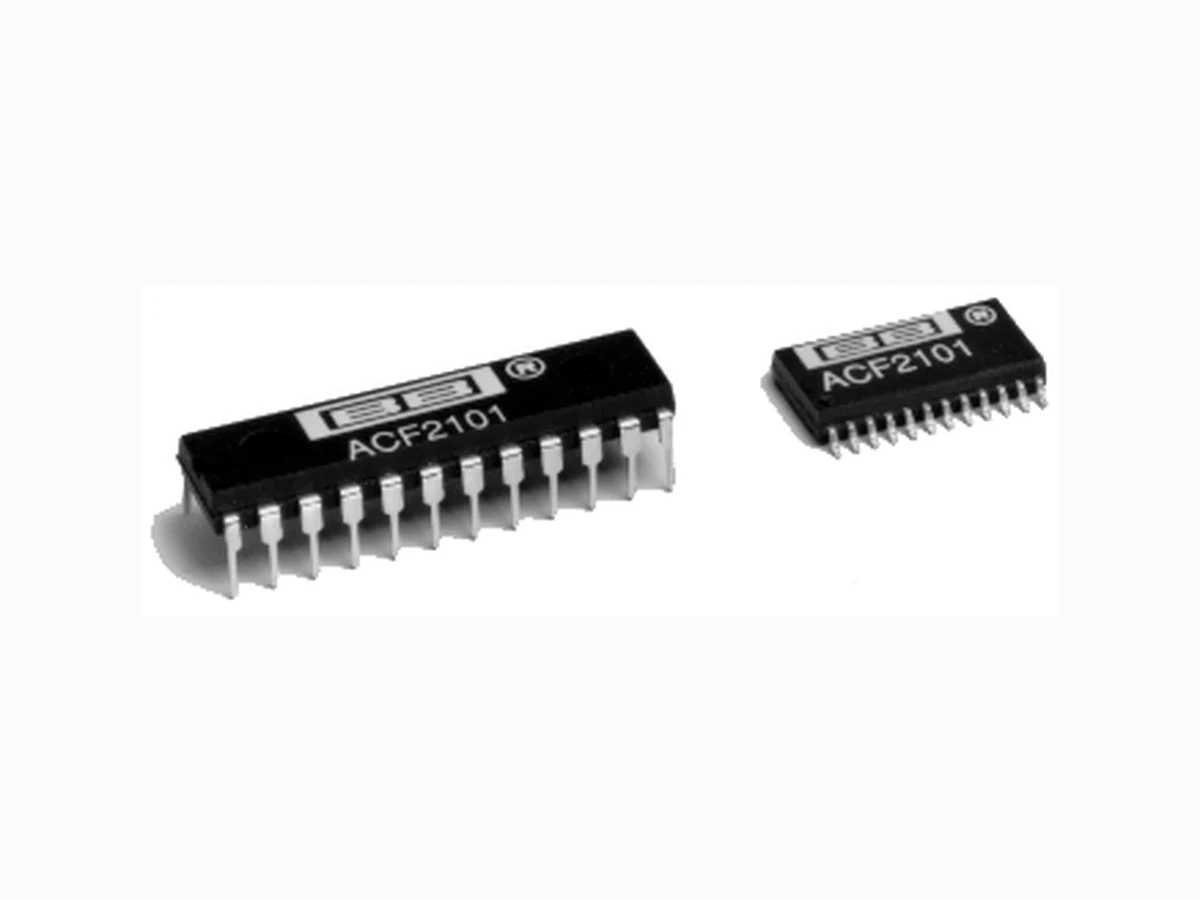
The ACF2101 is a dual switched integrator for preci- sion applications. Each channel can convert an input current to an output voltage by integration, using either an internal or external capacitor. Included on the chip are precision 100pF integration capacitors, hold and reset switches, and output multiplexers. As a complete circuit on a single chip, the ACF2101 eliminates many of the problems commonly encoun- tered in discrete designs, such as leakage current errors and noise pickup. The integrating approach can pro- vide lower noise than conventional transimpedance amplifier designs and also eliminates the need for high performance, high value feedback resistors. The extremely low bias current and low noise of the ACF2101’s Difet® amplifiers, along with active la- ser trimming of both offset and drift, assure precision current to voltage conversion. Although designed for +5V, –15V supplies, the ACF2101 can be operated on supplies up to ±18VDC. It is available in both 24-pin plastic DIP and SOIC packages. Difet® Burr-Brown Corp.
FEATURES
G INCLUDES INTEGRATION CAPACITOR, RESET AND HOLD SWITCHES, AND OUTPUT MULTIPLEXER G LOW NOISE: 10 µVrms G LOW CHARGE TRANSFER: 0.1pC G WIDE DYNAMIC RANGE: 120dB G LOW BIAS CURRENT: 100fA FPO © 1990 Burr-Brown Corporation PDS-1078D Printed in U.S.A. September, 1994 SBFS003
VOUT = – IINdt SPECIFICATIONS ELECTRICAL At TA = +25°C, V+ = +5V, V– = –15V, Internal CINTEGRATION = CINTERNAL = 100pF, unless otherwise noted. C INTEGRATION The information provided herein is believed to be reliable; however, BURR-BROWN assumes no responsibility for inaccuracies or omissions. BURR-BROWN assumes no responsibility for the use of this information, and all use of such information shall be entirely at the user’s own risk. Prices and specifications are subject to change without notice. No patent rights or licenses to any of the circuits described herein are implied or granted to any third party. BURR-BROWN does not authorize or warrant any BURR-BROWN product for use in life support devices and/or systems. ACF2101BP, BU PARAMETER CONDITIONS MIN TYP MAX UNITS ANALOG INPUT INPUT RANGE Input Current Range Switched Input (S W IN A, SW IN B) ±100 µA Direct Input (IN A, IN B) ±100 µA INPUT IMPEDANCE Switched Input Hold Switch OFF 1000 G Ω Hold Switch ON 1.5 k Ω Direct Input Virtual Ground HOLD SWITCH VOLTAGE Hold Switch Withstand Voltage Hold Switch OFF –10 +0.5 V OFFSET VOLTAGE Input Offset Voltage ±0.5 ±2m V Average Drift ±1 ±5 µV/°C DIGITAL INPUTS Logic Family TTL Compatible V IH (Logic 1 = Switch OFF) 2 5.5 V VIL (Logic 0 = Switch ON) –0.5 0.8 V IIH VIH = +5V 2 µA IIL VIL = 0V 0 µA Switching Speed (All Switches) Switch ON 200 ns Switch OFF 200 ns TRANSFER CHARACTERISTICS TRANSFER FUNCTION V DYNAMIC CHARACTERISTICS Integrate Mode Slew Rate 13 V / µs Reset Mode Slew Rate 3V / µs Settling Time to 0.01%FSR(1) 10V Step 5 10 µs Overload Recovery Positive or Negative 5 µs Output Multiplexer (Select Switches) Settling Time to 0.01%FSR C LOAD < 1000pF 6.5 µs Settling Time to 0.01%FSR C LOAD < 100pF 2 µs INTEGRATION CAPACITOR (C INTERNAL ) Internal Capacitor Value 100 pF Accuracy 0.5 2 % Temperature Coefficient –50 –25 0 ppm/ °C Memory 30 100 ppm of FSR RESET SWITCH Impedance Reset OFF 1000 G Ω Reset ON 1.5 k Ω MODES OF OPERATION Switch Hold Reset Integrate Mode ON OFF Hold Mode OFF OFF Reset Mode ON/OFF ON (Logic 1 = OFF, Logic 0 = ON)
SPECIFICATIONS (CONT) At TA = +25°C, V+ = +5V, V– = –15V, Internal CINTEGRATION = CINTERNAL = 100pF, unless otherwise noted. ACF2101BP, BU PARAMETER CONDITIONS MIN TYP MAX UNITS OUTPUT Voltage Output Range (All Outputs) –10 –13.5, +1.0 +0.5 V Current Output, Direct Output (Out A, Out B) ±5m A Short Circuit Current Direct Output ±25 mA Switched Output (Sw Out A, Sw Out B) ±2 ±8m A Select Switch Withstand Voltage Switched Output –10 +0.5 V Switched Common (Sw Com A, Sw Com B) –0.5 +0.5 V Output Impedance Direct Output 0.1 Ω Switched Output Select Switch ON 250 || 5 Ω || pF Select Switch OFF 1000 || 4 G Ω || pF Leakage Current Select Switch OFF 10 100 pA Load Capacitance Stability Direct Output 500 pF Switched Output Any pF OUTPUT ACCURACY Nonlinearity ±0.005 ±0.01 %FSR Channel Separation –80 dB Op Amp Bias Current Value 100 1000 fA Temperature Coefficient Doubles Each +10°C Hold Mode Droop 1 10 nV/ µs Integrate Mode Droop 1 10 nV/ µs Voltage Offset(2) Value 3m V Temperature Coefficient 5 µV/°C Power Supply Rejection V S = +4.5V to +18V, –10V to –18V 80 100 dB OUTPUT NOISE Total Output Noise(3) BW = 0.1Hz to 10Hz 2 µVrms Integrate Mode(4) BW = 0.1Hz to 250kHz 10(1 + C IN/CINTEGRATION ) µVrms Hold Mode BW = 0.1Hz to 250kHz 10 µVrms Reset Mode BW = 0.1Hz to 250kHz 10 µVrms CHARGE TRANSFER ERRORS (5) Reset to Integrate Mode(6) Charge Transfer 0.1 0.5 pC Charge Transfer TC 0.2 fC/ °C Charge Offset Error 15 m V Charge Offset TC 2 µV/°C Integrate to Hold Mode C IN > 50pF Charge Transfer 0.2 1 pC Charge Transfer TC 0.4 fC/ °C Charge Offset Error 21 0 m V Charge Offset TC 4 µV/°C Hold to Integrate Mode C IN > 50pF Charge Transfer 0.2 1 pC Charge Transfer TC 0.4 fC/ °C Charge Offset Error 21 0 m V Charge Offset TC 4 µV/°C POWER SUPPLY Specified Operating Voltage +5, –15 V Operating Voltage Range Positive Supply +4.5 +18 V Negative Supply –10 –18 V Current Positive Supply For Dual 12 15 mA Negative Supply For Dual 3.5 5.2 mA TEMPERATURE RANGE Specification –40 +85 °C Operation –40 +125 °C Storage –40 +125 °C Thermal Resistance (both packages) Junction to Ambient 100 °C/W NOTES: (1) FSR is Full Scale Range = 10V (0 to –10V). (2) Includes offset errors from all modes of operation. (3) Total noise is rms total of noise for the modes of operation used. (4) C IN = capacitance of sensor connected to ACF2101 input; CINTERGRATION = integration capacitance = CINTERNAL + CEXTERNAL . (5) Errors created when the internal switches are driven from one mode to another. (6) The charge transfer is 0.1pC; for an integration capacitance of 100pF, the resultant charge offset voltage error is 1mV.
Electrostatic discharge can cause damage ranging from per- formance degradation to complete device failure. Burr- Brown Corporation recommends that all integrated circuits be handled and stored using appropriate ESD protection methods. PACKAGE DRAWING TEMPERATURE PRODUCT PACKAGE NUMBER (1) RANGE ACF2101BP 24-Pin Plastic DIP 243 –40°C to +85°C ACF2101BU 24-Pin Plastic SOIC 239 –40°C to +85°C NOTE: (1) For detailed drawing and dimension table, please see end of data sheet, or Appendix C of Burr-Brown IC Data Book. PACKAGE/ORDERING INFORMATION TOP VIEW ACF2101BU PIN CONFIGURATION DIP and SOIC package have different pinouts. TOP VIEW ACF2101BP DIP Out A Gnd A Com A Cap A In A Sw In A Sw In B In B Cap B Com B Gnd B Out B Sw Out A Sw Com A Select A Reset A Hold A Hold B Reset B Select B Sw Com B Sw Out B Sw In B In B Cap B Com B Gnd B Out B Sw Out B Sw Com B Select B Reset B Hold B Sw In A In A Cap A Com A Gnd A Out A Sw Out A Sw Com A Select A Reset A Hold A SOIC
13 B Switch-Out
14 B Switch-Common
15 B Select
16 B Reset
17 B Hold
18 V –
20 A Hold
21 A Reset
22 A Select
23 A Switch-Common
24 A Switch-Out
2 A Ground
3 A Common
5 A In
6 A Switch-In
7 B Switch-In
8 B In
10 B Common
11 B Ground
12 B Out
Substrate Bias: Ground. MECHANICAL INFORMATION MILS (0.001") MILLIMETERS Die Size 132 x 157 ±5 3.35 x 3.99 ±0.13 Die Thickness 20 ±3 0.51 ±0.08 Min. Pad Size 4 x 4 0.10 x 0.10 Backing None ACF2101 DIE TOPOGRAPHY
R ON (Ω ) RESET SWITCH R ON vs INPUT CURRENT 1.65k 1.6k 1.55k 1.4k 1.35k –10µA–100µA –1µA 0 1µA 10µA 100µA 1.5k 1.45k NOTE: If IIN flows through Reset Switch that is ON, an output offset voltage is created. Reset SW R ONIIN IIN R ON (Ω ) HOLD SWITCH R ON vs INPUT CURRENT 1.65k 1.6k 1.55k 1.4k 1.35k –10µA–100µA –1µA 0 1µA 10µA 100µA 1.5k 1.45k IIN Hold SW R ON C LOAD (pF) Sw Out Settling Time (µs) to 0.01%, 10V Step Sw Out SETTLING TIME vs CLOAD 1000 300 200 500 400 700 600 900 800 1000 C INTEGRATION (pF) Reset Time to 0.01% (µs) RESET TIME vs CINTEGRATION 1000 300 200 500 400 700 600 900 800 1000 TOTAL OUTPUT NOISE vs C 1 and C2 100 C 1 (pF) 100 200 300 400 500 600 700 800 900 1000 Total Output Noise (µVrms) C 2 = 200pF C 2 = 500pF C 2 = 1000pF C 2 = 100pF Temperature (°C) Op Amp Bias Current 10pA 1pA 100fA 10fA –20–40 20 06 0 40 80 100 BIAS CURRENT vs TEMPERATURE TYPICAL PERFORMANCE CURVES At TA = +25°C, V+ = +5V, V– = –15V, CINTEGRATION = CINTERNAL = 100pF, unless otherwise noted.
FIGURE 1c. Circuit Connections with External Capacitors and Guarding, SOIC package . FIGURE 1d. Circuit Connections with External Capacitors and Guarding, DIP . FIGURE 2b. PC Board Layout Showing “Guard” Traces for Input, DIP . Both top and bottom of board should be guarded. FIGURE 2a. PC Board Layout Showing “Guard” Traces for Input, SOIC package . Both top and bottom of board should be guarded. Top View ACF2101BU Top View ACF2101BP ACF2101BU ACF2101BP Guards Sw In A 24 In A 23 Cap A 22 Com A 21
1 Sw In B
2 In B
3 Cap B
4 Com B
3 Com A
4 Cap A
5 In A
6 Sw In A
7 Sw In B
8 In B
9 Cap B
10 Com B
1µF 1µF Input Input * Optional External C Guards These points must be connected to a common ground point or a ground plane. VOUT VOUT SOIC Out A Gnd A Com A Cap A In A Sw In A Sw In B In B Cap B Com B Gnd B Out B Input Optional External C Guards These points must be connected to a common ground point or a ground plane. VOUT Input VOUT DIP 1µF 1µF
capacitor when the Hold and Reset switches change mode. compensated to reduce charge transfer errors. charge offset and 200pF in a 0.5mV charge offset. Bias Current vs Temperature.
100 X 10
FIGURE 8. Droop and Charge Offset Effects. requiring the full bandwidth of the ACF2101. ured to convert a low level input current to an output voltage. of noise such as power line pickup. 100pF are used with the ACF2101.
FIGURE 12. Using the ACF2101 with a Voltage Source.
www.ti.com 29-Jan-2026 PACKAGING INFORMATION Orderable part number Status (1) Material type (2) Package | Pins Package qty | Carrier RoHS (3) Lead finish/ Ball material (4) MSL rating/ Peak reflow (5) Op temp (°C) Part marking (6) ACF2101BU Last Time Buy Production SOIC (DW) | 24 25 | TUBE Yes NIPDAU Level-3-260C-168 HR -40 to 125 ACF2101BU ACF2101BU.A NRND Production SOIC (DW) | 24 25 | TUBE Yes NIPDAU Level-3-260C-168 HR -40 to 125 ACF2101BU (1) Status: For more details on status, see our product life cycle. (2) Material type: When designated, preproduction parts are prototypes/experimental devices, and are not yet approved or released for full production. Testing and final process, including without limitation quality assurance, reliability performance testing, and/or process qualification, may not yet be complete, and this item is subject to further changes or possible discontinuation. If available for ordering, purchases will be subject to an additional waiver at checkout, and are intended for early internal evaluation purposes only. These items are sold without warranties of any kind. (3) RoHS values: Yes, No, RoHS Exempt. See the TI RoHS Statement for additional information and value definition. (4) Lead finish/Ball material: Parts may have multiple material finish options. Finish options are separated by a vertical ruled line. Lead finish/Ball material values may wrap to two lines if the finish value exceeds the maximum column width. (5) MSL rating/Peak reflow: The moisture sensitivity level ratings and peak solder (reflow) temperatures. In the event that a part has multiple moisture sensitivity ratings, only the lowest level per JEDEC standards is shown. Refer to the shipping label for the actual reflow temperature that will be used to mount the part to the printed circuit board. (6) Part marking: There may be an additional marking, which relates to the logo, the lot trace code information, or the environmental category of the part. Multiple part markings will be inside parentheses. Only one part marking contained in parentheses and separated by a "~" will appear on a part. If a line is indented then it is a continuation of the previous line and the two combined represent the entire part marking for that device. Important Information and Disclaimer:The information provided on this page represents TI's knowledge and belief as of the date that it is provided. TI bases its knowledge and belief on information provided by third parties, and makes no representation or warranty as to the accuracy of such information. Efforts are underway to better integrate information from third parties. TI has taken and continues to take reasonable steps to provide representative and accurate information but may not have conducted destructive testing or chemical analysis on incoming materials and chemicals. TI and TI suppliers consider certain information to be proprietary, and thus CAS numbers and other limited information may not be available for release. In no event shall TI's liability arising out of such information exceed the total purchase price of the TI part(s) at issue in this document sold by TI to Customer on an annual basis. Addendum-Page 1
PACKAGE MATERIALS INFORMATION www.ti.com 10-Aug-2026 TUBE L - Tube length T - Tube height W - Tube width B - Alignment groove width *All dimensions are nominal Device Package Name Package Type Pins SPQ L (mm) W (mm) T (µm) B (mm) ACF2101BU DW SOIC 24 25 507 12.83 5080 6.6 ACF2101BU.A DW SOIC 24 25 507 12.83 5080 6.6 Pack Materials-Page 1
IMPORTANT NOTICE AND DISCLAIMER TI PROVIDES TECHNICAL AND RELIABILITY DATA (INCLUDING DATASHEETS), DESIGN RESOURCES (INCLUDING REFERENCE DESIGNS), APPLICATION OR OTHER DESIGN ADVICE, WEB TOOLS, SAFETY INFORMATION, AND OTHER RESOURCES “AS IS” AND WITH ALL FAULTS, AND DISCLAIMS ALL WARRANTIES, EXPRESS AND IMPLIED, INCLUDING WITHOUT LIMITATION ANY IMPLIED WARRANTIES OF MERCHANTABILITY, FITNESS FOR A PARTICULAR PURPOSE OR NON-INFRINGEMENT OF THIRD PARTY INTELLECTUAL PROPERTY RIGHTS. These resources are intended for skilled developers designing with TI products. You are solely responsible for (1) selecting the appropriate TI products for your application, (2) designing, validating and testing your application, and (3) ensuring your application meets applicable standards, and any other safety, security, regulatory or other requirements. These resources are subject to change without notice. TI grants you permission to use these resources only for development of an application that uses the TI products described in the resource. Other reproduction and display of these resources is prohibited. No license is granted to any other TI intellectual property right or to any third party intellectual property right. TI disclaims responsibility for, and you fully indemnify TI and its representatives against any claims, damages, costs, losses, and liabilities arising out of your use of these resources. TI’s products are provided subject to TI’s Terms of Sale, TI’s General Quality Guidelines, or other applicable terms available either on ti.com or provided in conjunction with such TI products. TI’s provision of these resources does not expand or otherwise alter TI’s applicable warranties or warranty disclaimers for TI products. Unless TI explicitly designates a product as custom or customer-specified, TI products are standard, catalog, general purpose devices. TI objects to and rejects any additional or different terms you may propose. IMPORTANT NOTICE Copyright © 2026, Texas Instruments Incorporated Last updated 10/2025