
 Download PDF
ACF2101 BURR-BROWN
Document overview
- PDF pages: 14
Technical content
Page 1
Page 2
SPECIFICATIONS
ELECTRICAL
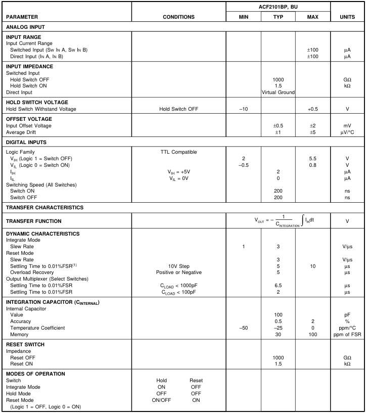
At TA = +25°C, V+ = +5V, V– = –15V, Internal CINTEGRATION = CINTERNAL = 100pF, unless otherwise noted.
The information provided herein is believed to be reliable; however, BURR-BROWN assumes no responsibility for inaccuracies or omissions. BURR-BROWN assumes no responsibility for the use of this information, and all use of such information shall be entirely at the user’s own risk. Prices and specifications are subject to change without notice. No patent rights or licenses to any of the circuits described herein are implied or granted to any third party. BURR-BROWN does not authorize or warrant any BURR-BROWN product for use in life support devices and/or systems.
Page 3
SPECIFICATIONS (CONT)
At TA = +25°C, V+ = +5V, V– = –15V, Internal CINTEGRATION = CINTERNAL = 100pF, unless otherwise noted.
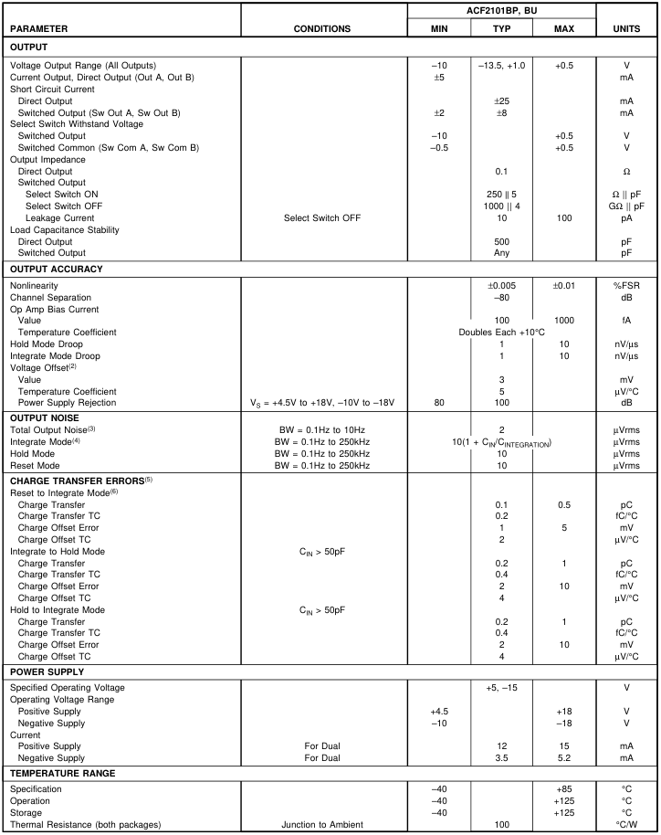
NOTES: (1) FSR is Full Scale Range = 10V (0 to –10V). (2) Includes offset errors from all modes of operation. (3) Total noise is rms total of noise for the modes of operation used. (4) CIN = capacitance of sensor connected to ACF2101 input; CINTERGRATION = integration capacitance = CINTERNAL + CEXTERNAL. (5) Errors created when the internal switches are driven from one mode to another. (6) The charge transfer is 0.1pC; for an integration capacitance of 100pF, the resultant charge offset voltage error is 1mV.
Page 4
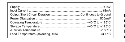
ABSOLUTE MAXIMUM RATINGS
PACKAGE/ORDERING INFORMATION
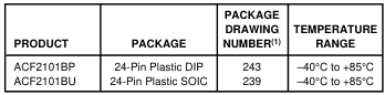
NOTE: (1) For detailed drawing and dimension table, please see end of data sheet, or Appendix C of Burr-Brown IC Data Book.
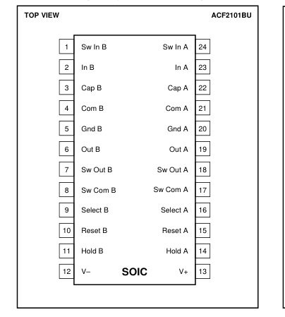
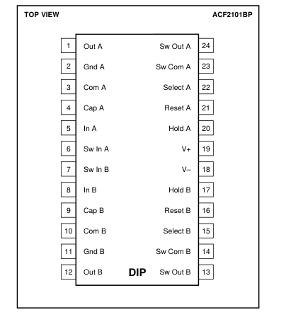
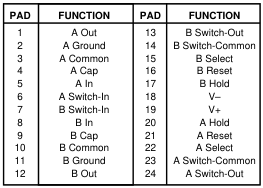
PIN CONFIGURATION DIP and SOIC package have different pinouts.
ELECTROSTATIC
DISCHARGE SENSITIVITY
Electrostatic discharge can cause damage ranging from per-
formance degradation to complete device failure. Burr-
Brown Corporation recommends that all integrated circuits
be handled and stored using appropriate ESD protection
methods.
Page 5
DICE INFORMATION
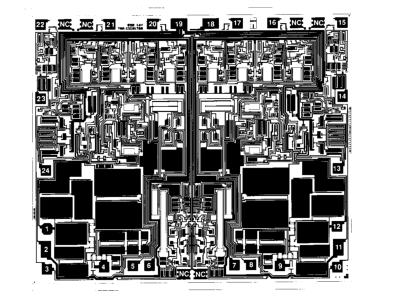
Substrate Bias: Ground.
MECHANICAL INFORMATION
| MILS (0.001") | MILLIMETERS | |
| Die Size Die Thickness Min. Pad Size | 132 x 157 ±5 20 ±3 4 x 4 | 3.35 x 3.99 ±0.13 0.51 ±0.08 0.10 x 0.10 |
| Backing None | ||
ACF2101 DIE TOPOGRAPHY
Page 6
TYPICAL PERFORMANCE CURVES
At TA = +25°C, V+ = +5V, V– = –15V, CINTEGRATION = CINTERNAL = 100pF, unless otherwise noted.
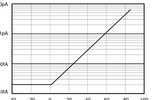
BIAS CURRENT vs TEMPERATURE
100fA
–40 –20 0 20 40 60 80 100
Temperature (°C)
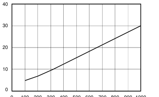
RESET TIME vs CINTEGRATION
0 100 200 300 400 500 600 700 800 900 1000
CINTEGRATION (pF)
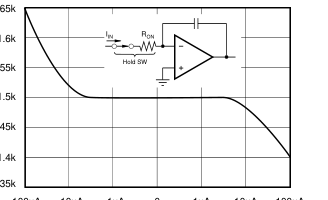
HOLD SWITCH RON vs INPUT CURRENT
1.65k
1.55k
1.45k
1.35k –100µA –10µA –1µA
0 1µA 10µA 100µA
IIN
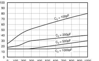
TOTAL OUTPUT NOISE vs C1 and C2
0 100 200 300 400 500 600 700 800 900 1000
C1 (pF)
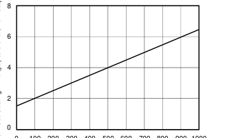
Sw Out SETTLING TIME vs CLOAD
0 100 200 300 400 500 600 700 800 900 1000
CLOAD (pF)
RESET SWITCH RON vs INPUT CURRENT
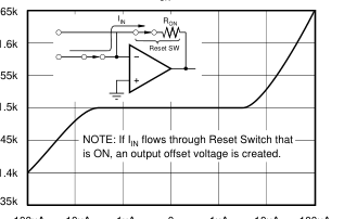
1.65k
1.55k
1.45k
1.35k –100µA –10µA –1µA
0 1µA 10µA 100µA
IIN
Page 7
APPLICATIONS INFORMATION
BASIC CIRCUIT CONNECTION
Basic Layout As with any precision circuit, careful layout will ensure best performance. Make short, direct interconnections and avoid stray wiring capacitance—especially at the analog and digital input pins. Figures 1a and 1b illustrate the basic connections needed for operation. Figures 1c and 1d illustrate the addition of external integration capacitors and input guards. Leakage currents between printed circuit board traces can easily exceed the input bias current of the ACF2101. A circuit board “guard” pattern reduces leakage effects by surrounding critical high impedance input circuitry with a low impedance circuit connection at the same potential. Leakage will flow harmlessly to the low impedance node.
Figure 2a and 2b show printed circuit patterns that can be used to guard critical pins. Note that traces leading to these pins should also be guarded.
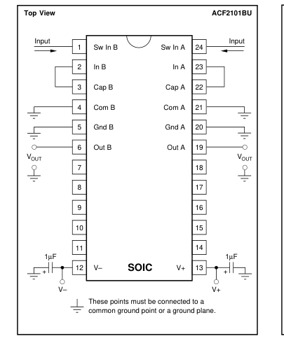
FIGURE 1a. Basic Circuit Connections, SOIC package.
Improper handling or cleaning may increase droop. Contamination from handling parts and circuit boards can be removed with cleaning solvents and de-ionized water.
Pinout The pinout for the DIP and SOIC package of the ACF2101 is different. The pinouts for the different packages are shown in several figures in this data sheet.
Power Supplies The ACF2101 can operate from supplies that range from +4.5V and –10V to ±18V. Since the output voltage integrates negatively from ground, a positive supply of +5V is sufficient to attain specified performance. Using +5V and –15V power supplies reduces power dissipation by one-half of that at ±15V. Power supply connections should be bypassed with good high-frequency capacitors, such as 1µF solid tantalum capacitors, positioned close to the power supply pins.
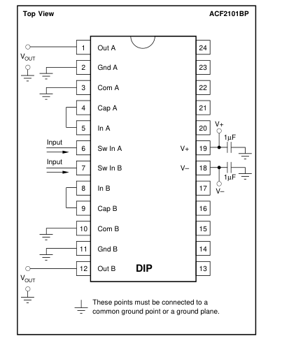
FIGURE 1b. Basic Circuit Connections, DIP.
Page 8
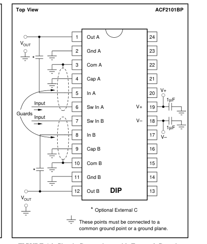
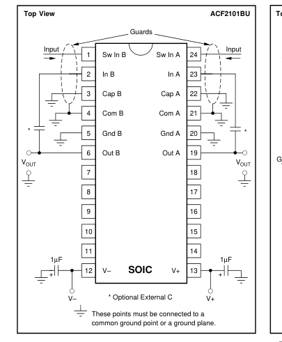
FIGURE 1d. Circuit Connections with External Capacitors
FIGURE 1c. Circuit Connections with External Capacitors
and Guarding, DIP.
and Guarding, SOIC package.
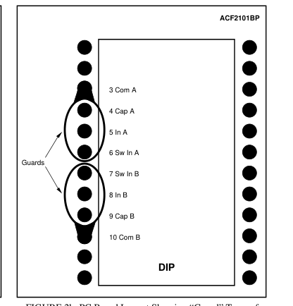
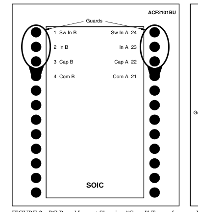
FIGURE 2a. PC Board Layout Showing “Guard” Traces for
Input, SOIC package. Both top and bottom of
board should be guarded.
FIGURE 2b. PC Board Layout Showing “Guard” Traces for
Input, DIP. Both top and bottom of board
should be guarded.
Page 9
MODES OF OPERATION
The three basic modes of operation of each integrator are controlled by the Hold and Reset switches. In Integrate mode, the output voltage integrates negatively toward –10V. In Hold mode, the output voltage remains at the present value, except for output droop. In Reset mode, the integration capacitor is discharged and the output voltage is driven to analog common. See Figure 4.
SWITCHES
Each integrator includes four switches: a Hold switch, a Reset switch, and two output Select switches. See Figure 3.
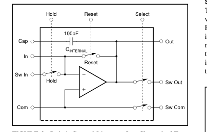
FIGURE 3. Switch Control Lines on One Channel of Two in ACF2101.
| HOLD INTEGRATE HOLD RST HOLD INTEGRATE 0 (V) OUTPUT –10 OFF HOLD ON OFF RESET ON MODES OF OPERATION | |||
| SWITCH | MODE OF OPERATION Integrate Hold Reset | ||
| Hold Switch Reset Switch | ON OFF | OFF OFF | ON/OFF ON |
| ON: Switch shorted; Logic 0 input. OFF: Switch open; Logic 1 input. | |||
FIGURE 4. Modes of Operation.
Hold and Reset Switches To use the Hold switch, connect the input current to the “Sw In” pin. The Hold switch disconnects the input current, and holds the output voltage at a fixed level. For direct input, connect the input current to the “In” pin that bypasses the Hold switch and connects directly to the input summing junction. If the Hold switch is not used, the switch should be in the off mode and the “Sw In” pin should be connected to analog common. The Reset switch is used to discharge the integration capacitor before the start of a new integration period. See Typical Performance Curve showing Reset Time vs CINTEGRATION. Select Switches The two Select switches can be used to multiplex the outputs
when multiple integrators are connected to a common bus. Figure 5 shows a number of ACF2101s multiplexed together into an A/D converter. The output settling time is determined by the Select switch “on” resistance of 250Ω and the total output capacitance. The total output capacitance includes the ACF2101 output capacitances plus the capacitance of the interconnections to the A/D converter.
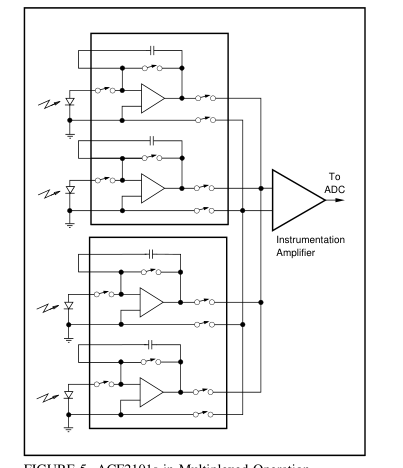
FIGURE 5. ACF2101s in Multiplexed Operation.
Page 10
OUTPUT VOLTAGE
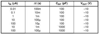
The integrator output voltage range is from +0.5V to –10V. The output voltage (VOUT) can be calculated as:
VOUT = IIN x ∆t CINT
VOUT = the maximum output voltage (in volts) CINT = the integration capacitance (in farads) IIN = the input current (in amperes) ∆t = the integration time (in seconds)
Examples of Component Values for –10V Output
OUTPUT OVERLOAD
When the output to the ACF2101 integrates to the negative limit, the output voltage smoothly limits at approximately 1.5V from the negative power supply, and reset time will increase by approximately 5µs for overload recovery. For fastest reset time avoid integrating to the negative limit.
EXTERNAL CAPACITOR
An external integration capacitor may be used instead of or in addition to the internal 100pF integration capacitor. Since the transfer function depends upon the characteristics of the integration capacitor, it must be carefully selected. An external integration capacitor should have low voltage coefficient, temperature coefficient, memory, and leakage current. The optimum selection depends upon the requirements of the specific application. Suitable types include NPO ceramic, polycarbonate, polystyrene, and silver mica. If the internal integration capacitor is not used, the Cap pin should be connected to common.
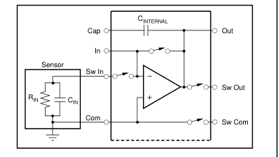
FIGURE 6. Capacitance of Circuit at Input of Integrator.
NOISE
The total output noise for a specific application of the ACF2101 is the rms total of the noise in the modes used: Integrate noise (enI), Hold noise (enH) and Reset noise (enR). The noise in both the Hold (enH) and Reset (enR) modes is 10µVrms. The noise in the Integrate mode (enI) is directly proportional to one plus the ratio of CIN to CINTEGRATION, where CIN is the capacitance of the circuit at the input of the integrator and CINTEGRATION = CINTERNAL + CEXTERNAL and is the integration capacitance: Integrate output noise (enI) = (10µVrms) x (1 + CIN/CINTEGRATION) Therefore, for very low CIN, the Integrate noise will ap- proach 10µVrms. The total noise when in the Hold mode
after proceeding through Reset and Integrate modes is approximated as shown below.
Total Noise = enI2 + enH2 + enR
2
See Typical Performance Curve showing Total Output Noise vs CIN and CINTEGRATION for more accurate noise data under specific circumstances. If only the Integrate and Reset modes are used, the total noise is the rms sum of the noise of the two modes as shown below.
enI2 + enR 2
Total Noise =
DYNAMIC CHARACTERISTICS
Frequency Response The ACF2101 switched integrator is a sampled system controlled by the sampling frequency (fs), which is usually dominated by the integration time. Input signals above the Nyquist frequency (fs/2) create errors by being aliased into the sampled frequency bandwidth. The sampled frequency bandwidth of the switched integrator has a –3dB characteristic at fs/2.26 and a null at fs and harmonics 2fs, 3fs, 4fs, etc. This characteristic is often used to eliminate known interference.
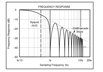
FIGURE 7. Frequency Response.
Page 11
Charge Transfer Charge transfer is the charge that is coupled from the logic control inputs through circuit capacitance to the integration capacitor when the Hold and Reset switches change mode. Careful printed circuit layout must be used to minimize external coupling from digital to analog circuitry and the resulting charge transfer. Charge transfer results in a DC charge offset error voltage. The ACF2101 switches are compensated to reduce charge transfer errors. Since the ACF2101 switches contribute equal and opposite charge for positive and negative logic input transitions, the total error due to charge transfer is determined by the switching sequence. For each switch, a logic transition
results in a specific charge (and offset voltage) while an opposite going logic transition results in an opposite charge (and opposite offset voltage). Thus, if the Hold switch is turned on and off during one integration cycle, the total charge transfer at the end of the sequence due to the Hold switch is essentially zero. The amount of charge transfer to the integration capacitor is constant for each switch. Therefore, the charge offset error voltage is lower for larger integration capacitors. The ACF2101’s 0.1pC charge transfer results in a 1mV charge offset voltage when using the 100pF internal integration capacitor. The offset voltage will change linearly with the
integration capacitance. That is, 50pF will result in a 2mV charge offset and 200pF in a 0.5mV charge offset.
Droop Droop is the change in the output voltage over time as a result of the bias current of the amplifier, leakage of the integration capacitor and leakage of the Reset and Hold switches. Droop occurs in both the Integrate and Hold modes of operation. Careful printed circuit layout must be used to minimize external leakage currents as discussed previously. The droop is calculated by the equation:
100fA Droop = CINTEGRATION
where CINTEGRATION = CINTERNAL + CEXTERNAL and is the integration capacitance in farads and the result is in volts per second. For the internal integration capacitance of 100pF, the droop is calculated as:
–15 100 X 10 Droop = = 1mV/s or 1nV/µs
–12 100 X 10
Droop increases by a factor of 2 for each 10°C increase above 25°C. See the typical performance curve showing Bias Current vs Temperature.
Capacitive Loads Any capacitive load can be safely driven through the multiplexed output of the ACF2101. As with any op amp, however, best dynamic performance of the ACF2101 can be achieved by minimizing the capacitive load. See the typical performance curve showing settling time as a function of capacitive load for more information. A large capacitive
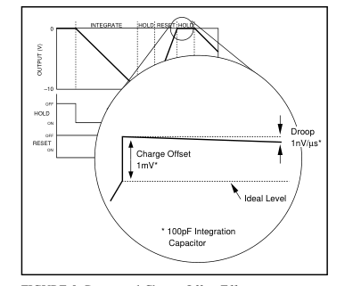
FIGURE 8. Droop and Charge Offset Effects.
load is often useful in reducing the noise of systems not requiring the full bandwidth of the ACF2101.
PROGRAMMABLE I TO V CONVERTER EXAMPLE
Figure 10 illustrates the use of the ACF2101 as a programmable current to voltage converter. The output of the circuit, VOUT, is a DC level for a constant current input. The timing diagram shown in Figure 9 shows VOUT for an input current that varies from one sample to the next. This circuit offers wide dynamic range without the use of extremely large resistors. An ACF2101 and an OPA2107 op amp are configured to convert a low level input current to an output voltage. The equivalent gain of the converter is determined by the frequency of the digital input signal, fS. The inherent integrating function of the ACF2101 is very useful for rejection of noise such as power line pickup.
The ACF2101 integrates the current signal for the period of fS. The magnitude of the ramp voltage at the output of the ACF2101 is a function of the frequency of fS and the value of the integration capacitor, CINTEGRATION. The ACF2101’s 100pF internal capacitor is used for CINTEGRATION in this example. The effect is that fS controls the equivalent feedback resistance of a transconductance (current-to-voltage) amplifier. The equivalent feedback resistance range can vary over a large range of at least 1MΩ to 1GΩ as illustrated in the accompanying table. Larger equivalent feedback resistances can be obtained if internal capacitances smaller than 100pF are used with the ACF2101.
A simplified equation for the operation of this circuit is:
VOUT = ISENSOR X RPROGRAM
Where: VOUT is the voltage at the output of the OPA2107, ISENSOR is the current into the ACF2101, and RPROGRAM is the equivalent feedback resistance of the circuit calculated by the equation, RPROGRAM = 1/(fS X CINTEGRATION) = 1/(fS X 100pF)
Page 12
For CINTEGRATION = 100pF, RPROGRAM is calculated below:
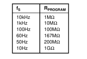
At the end of the integration cycle, the Hold switch of the ACF2101 is opened to hold a constant value at the output of the ACF2101. The constant value output voltage of the ACF2101 is transferred onto a 10nF capacitor by closing the ACF2101’s Select switch. The Select switch is then opened which holds the voltage on the 10nF capacitor during the next integration cycle and creates a DC output. With this operation, the Select switch of the ACF2101 and the 10nF capacitor form a Sample/Hold (S/H) circuit. The OPA2107 is used to buffer the Sample/Hold output. The charge injection of the Select switch creates a small offset voltage, of approximately 1mV in this example. The 10nF capacitor
was chosen as a large value to minimize this offset voltage. After the Select switch opens, the ACF2101 is reset by momentarily closing the Reset switch. The ACF2101’s Hold switch is then closed to begin another integration cycle. During the period of time that the Hold switch is open, the input signal current is stored on the input capacitance of the sensor (CIN). During this time, the input signal current creates a voltage across the sensor. This voltage should be kept below 500mV. When the Hold switch is closed, the charge that has collected on CIN will be transferred to the integration capacitor, CINTEGRATION, with no loss of signal. Therefore, one integration cycle ends and the next integra-
tion cycle begins when the Hold switch is opened. If 100% of signal acquisition is not required, or not wanted, the Hold switch may be left closed, or the direct input to the ACF2101 used. In this mode of operation, an integration cycle ends when the Select switch is opened and the next integration cycle begins when the Reset switch is opened.
Figure 11 shows a simple digital pattern generator which can be used to create the timing signals to control the ACF2101 circuit of Figure 10. This circuit creates signals to control the Select, Reset and Hold switches at a rate controlled by the frequency of fS. Figure 9 shows the timing diagram for these circuits. In a sampled data system, the output of the ACF2101 at the output of the Select switch can be converted to digital when the ACF2101 is in the Hold mode. In this situation, of course, the 10nF capacitor and the OPA2107 op amp are not required.
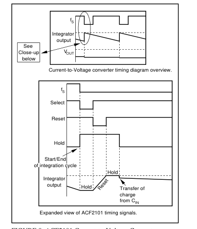
FIGURE 9. ACF2101 Current-to-Voltage Converter Timing Diagram.
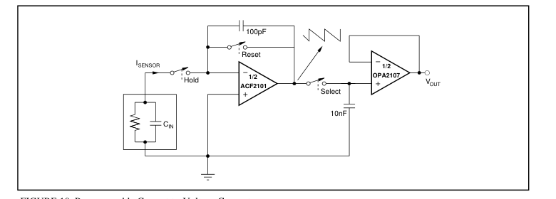
FIGURE 10. Programmable Current-to-Voltage Converter.
Page 13
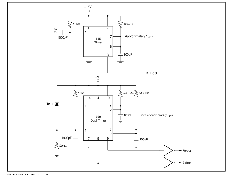
FIGURE 11. Timing Generator.
VOLTAGE INPUT EXAMPLE
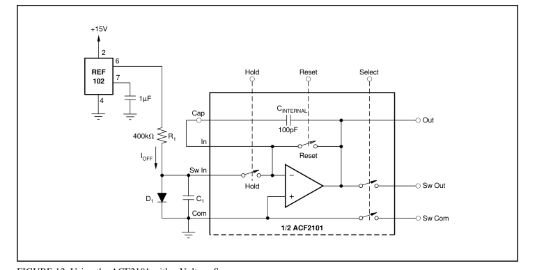
Figure 12 illustrates the use of the ACF2101 with a voltage input. This approach is useful in applications where a constant current source is needed. For example, the ACF2101 can be configured in a bipolar mode by using the current generated by a voltage reference as an offset current. In the example in Figure 12, a 10V reference (REF102) is used in series with a 400kΩ resistor to generate a constant +25µA input current to the ACF2101. The ACF2101 will operate as expected in this configuration except in the Hold mode. When the Hold switch is opened, the input to the ACF2101 becomes high impedance and consequently the Sw In node will try to go to 10V. The Hold switch is specified to have
a withstand voltage of +0.5V. When the voltage at the Sw In node exceeds +0.5V the Hold switch will begin to conduct again. This will not cause damage to the switch, however, the output will start to unexpectedly integrate again. The addition of either C1 or D1 in the circuit is critical for proper Hold mode operation. C1 will divert the charge being gener-
ated by the voltage source in series with the resistor. C1 is selected so that the maximum voltage does not exceed 0.4V. When the Hold switch is closed again, the charge collected by C1 is transferred to the integration capacitor. D1 will divert the charge being generated by the voltage source and resistor to ground. When the Hold switch closes again, the charge stored on the parasitic capacitor of the diode is transferred to the integration capacitor. D1 should be se- lected so that the on voltage of the diode does not exceed 0.4V.
DEMONSTRATION BOARD AND MACROMODEL
Demonstration boards are available to speed prototyping. The demonstration board, DEM-ACF2101BP-C includes a programmable timing generator making it easy to do a quick evaluation. A Spice-based macromodel is also available. Request AB-020 for Application Bulletin and Burr-Brown's Spice Macromodel diskette.
Page 14