


 Download PDF
DATASHEET SEARCH SITE
Document overview
- PDF pages: 10
Technical content
Page 1
DATA SHEET
ANTI-SULFURATED CHIP RESISTORS
AUTOMOTIVE GRADE
AA series ±5%, ±1%, ±0.5% sizes 0201/0402/0603/0805/1206/ 1210/1218/2010/2512 RoHS compliant & Halogen free
Page 2
2
SSC CO
OPPEE
ORRD
O DEERRIIN
NG
G IIN
NFFO
ORRM
MA
ATTIIO
ON N -- G
GLLO
OBBA
ALL PPA
ARRTT N
NU UM
MBBEERR
This specification describes AA0201 Part number is identified by the series name, size, tolerance, packaging
type, temperature coefficient, taping reel and resistance value.
to AA2512 chip resistors with leadfree terminations made by thick film
GLOBAL PART NUMBER
process.
AA XXXX X X X XX XXXX L
(1) (2) (3) (4) (5) (6) (7)
APPPPLLIIC
CA
ATTIIO
ON NSS
A Car electronics
(1) SIZE
Engine control unit
0201 / 0402 / 0603 / 0805 / 1206 / 1210 / 1218 / 2010 / 2512
Body control system
(2) TOLERANCE
Safety devices
D =±0.5% F = ±1%
FFEEA
ATTU
URREESS
J = ±5% (for Jumper ordering, use code of J)
Superior resistance against sulfur containing atmosphere
(3) PACKAGING TYPE
AEC-Q200 qualified
R = Paper/PE taping reel
K = Embossed taping reel
Moisture sensitivity level: MSL1
(4) TEMPERATURE COEFFICIENT OF RESISTANCE
AA series soldering is compliant with J-STD-020D
– = Base on spec
Halogen free epoxy
(5) TAPING REEL
RoHS compliant
07 = 7 inch dia. Reel
13 = 13 inch dia. Reel
Reduce environmentally
(6) RESISTANCE VALUE
hazardous waste
1Ω to 10 MΩ
High component and equipment
There are 2~4 digits indicated the resistance value. Letter R/K/M is decimal point, no
reliability
need to mention the last zero after R/K/M, e.g.1K2, not 1K20.
The resistors are 100% performed by automatic optical inspection
(7) DEFAULT CODE Letter L is the system default code for ordering only. (Note)
Resistance rule of global part number Resistance coding rule
XRXX (1 to 9.76 Ω)
XXRX (10 to 97.6 Ω) XXXR (100 to 976 Ω) XKXX (1 to 9.76 KΩ) XMXX (1 to 9.76 MΩ) XXMX (10 MΩ)
ORDERING EXAMPLE
The ordering code for an AA0402 chip resistor, value 100 KΩ with ±1%
Example
tolerance, supplied in 7-inch tape reel is: AA0402FR-07100KL
1R = 1 Ω 1R5 = 1.5 Ω
NOTE
9R76 = 9.76 Ω
- All our R-Chip products are RoHS
10R = 10 Ω
compliant and Halogen free. "LFP" of the internal 2D reel label states "Lead-Free
97R6 = 97.6 Ω
Process".
100R = 100 Ω
- On customized label, "LFP" or specific
976R = 976 Ω
symbol can be printed.
1K = 1,000 Ω 9K76 = 9760 Ω 1M = 1,000,000 Ω 9M76= 9,760,000 Ω
10M = 10,000,000 Ω
Page 3

MA
MARRKKIIN
NG G AA0201 / AA0402
No marking
Fig. 1
AA0603 / AA0805 / AA1206 / AA1210 / AA2010 / AA2512
E-24 series: 3 digits, ±5% First two digits for significant figure and 3rd digit for number of zeros
Fig. 2 Value=10 KΩ
AA0603
E-24 series: 3 digits, ±1% One short bar under marking letter
Fig. 3 Value = 24 Ω
E-96 series: 3 digits, ±1% First two digits for E-96 marking rule and 3rd letter for number of zeros
Fig. 4 Value = 12.4 KΩ
AA0805 / AA1206 / AA1210 / AA2010 / AA2512
Both E-24 and E-96 series: 4 digits, ±1% First three digits for significant figure and 4th digit for number of zeros
Fig. 5 Value = 10 KΩ
AA1218
E-24 series: 3 digits, ±5% First two digits for significant figure and 3rd digit for number of zeros
Fig. 6 Value = 10 KΩ
Both E-24 and E-96 series: 4 digits, ±1% First three digits for significant figure and 4th digit for number of zeros
Fig. 7 Value = 10 KΩ
NOTE
For further marking information, please refer to data sheet “Chip resistors marking”. Marking of AA series is the same as RC series.
Page 4

CO CON
NSSTTRRU
UC
CTTIIO
ON N
The resistors are constructed on top of an automotive
OU
UTTLLIIN
NEESS
O
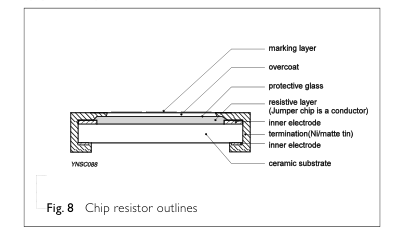
grade ceramic body. Internal metal electrodes are added at each end and connected by a resistive glaze. The resistive glaze is covered by a lead-free glass. The composition of the glaze is adjusted to give the approximately required resistance value and laser trimming of this resistive glaze achieves the value within tolerance. The whole element is covered by a protective overcoat. Size 0603 and bigger is marked with the resistance value on top. Finally, the two external terminations (Ni / matte tin) are added, as shown in Fig.8.
DIIM
D MEEN
NSSIIO
ON NSS
Table 1 For outlines, please refer to Fig. 9 TYPE
L (mm)
W (mm)
H (mm)
I1 (mm)
I2 (mm)
AA0201
0.60 ±0.03
0.30 ±0.03
0.23 ±0.03
0.12 ±0.05
0.15 ±0.05
AA0402
0.20 ±0.10
1.00 ±0.05
0.50 ±0.05
0.32 ±0.05
0.25 ±0.10
AA0603
0.25 ±0.15
1.60 ±0.10
0.80 ±0.10
0.45 ±0.10
0.25 ±0.15
AA0805
0.35 ±0.20
2.00 ±0.10
1.25 ±0.10
0.50 ±0.10
0.35 ±0.20
AA1206
0.45 ±0.20
3.10 ±0.10
1.60 ±0.10
0.55 ±0.10
0.40 ±0.20
AA1210
0.45 ±0.15
3.10 ±0.10
2.60 ±0.15
0.50 ±0.10
0.50 ±0.20
AA1218
0.45 ±0.20
3.10 ±0.10
4.60 ±0.10
0.55 ±0.10
0.40 ±0.20
AA2010
0.55 ±0.15
5.00 ±0.10
2.50 ±0.15
0.55 ±0.10
0.50 ±0.20
AA2512
6.35 ±0.10
3.10 ±0.15
0.55 ±0.10
0.60 ±0.20
0.50 ±0.20

Page 5
5
EELLEEC
CTTRRIIC
CA
ALL C
CH HA
ARRA
AC
CTTEERRIISSTTIIC
CSS

AA0201
25V
AA0402
50 V
5% (E24)
AA0603
75V
1Ω≤ R ≤ 22MΩ (0201: Max. 10MΩ.
AA0805
1218: Max. 1MΩ)
150 V
0.5%, 1% (E24/E96)
–55 °C to +155 °C
1Ω≤ R ≤10MΩ
AA1206
200 V
(1218: Max. 1MΩ) Jumper < 50mΩ
AA1210
200 V
AA1218
200 V
AA2010
200 V
AA2512
200 V
1Ω ≤ R ≤ 10Ω ,
Rated Current 0.5A
-100/+400 ppm/°C
50V
50V 10Ω < R ≤ 10 MΩ ,
Max. Current 1.0A
±300 ppm/°C
Rated Current
1A
100 V
100 V
Max. Current 2A Rated Current
1A
150 V
150 V
Max. Current 2A Rated Current
2A
300 V
300 V
Max. Current 5A
1 Ω ≤ R ≤ 10 Ω , ±200 ppm/°C Rated Current
2A
400 V
500 V
Max. Current 10A
10 Ω < R ≤ 10 MΩ , ±150 ppm/°C Rated Current
2A
500 V
500 V 10 MΩ < R ≤ 22 M Max. Current 10A Ω , ±200 ppm/°C Rated Current
6A
500 V
500 V
Max. Current 10A Rated Current
2A
500 V
500 V
Max. Current 10A Rated Current
2A
500 V
500 V
Max. Current 10A
Page 6
6
FFO OO
OTTPPRRIIN
NTT A
AN ND
D SSO
OLLD
DEERRIIN
NG
G PPRRO
OFFIILLEESS
Recommended footprint and soldering profiles. Please refer to data sheet “Chip resistors mounting”.
PPA AC
CKKIIN
NG
G SSTTYYLLEE A
AN ND
D PPA
AC
CKKA
AG
GIIN
NG G Q QU UA AN
NTTIITTYY
Table 3 Packing style and packaging quantity
REEL AA0201 AA0402 AA0603 AA0805 AA1206 AA1210 AA1218 AA2010 AA2512
PACKING STYLE
DIMENSION
Paper/PE taping reel 7" (178 mm) 10,000 10,000
5,000 5,000 5,000 5,000
--- --- ---
(R)
13" (330 mm) 50,000 50,000 20,000
20,000 20,000 20,000
--- --- ---
Embossed taping 7" (178 mm)
--- --- --- --- --- --- 4,000 4,000 4,000
reel (K)
TEMPERATURE COEFFICIENT OF RESISTANCE
RREESSIISSTTA
AN NC CEE
RRA AN NG GEE
NOTE
- For paper/PE/embossed tape and reel specifications/dimensions, please refer to data sheet “Chip resistors packing”.
100 mΩ to 910 mΩ
PT040 2
±200 ppm/°C
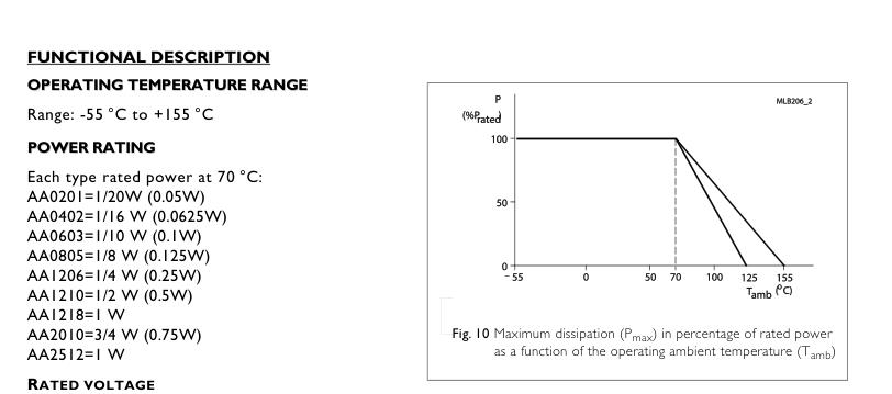
The DC or AA (rms) continuous working voltage corresponding to the rated power is determined by the following formula: V = √(P X R) Or Maximum working voltage whichever is less
Where V = Continuous rated DC or AA (rms) working voltage (V) P = Rated power (W)
R = Resistance value (Ω)
Page 7
7
TTEESSTTSS A
AN ND
D RREEQ
QU
UIIRREEM
MEEN
NTTSS
Table 4 Test condition, procedure and requirements TEST
TEST METHOD
PROCEDURE
REQUIREMENTS
1,000 hours at TA = 155 °C, unpowered
AEC-Q200 Test 3
±(1.0%+0.05Ω)
High Temperature Exposure
MIL-STD-202 Method 108
<50 mΩ for Jumper
Each temperature / humidity cycle is defined at
AEC-Q200 Test 6
±(0.5%+0.05Ω) for D/F tol.
Moisture
8 hours (method 106F), 3 cycles / 24 hours for
Resistance
MIL-STD-202 Method 106
±(2.0%+0.05Ω) for J tol.
10d. with 25 °C / 65 °C 95% R.H, without steps
<100 mΩ for Jumper
7a & 7b, unpowered Parts mounted on test-boards, without condensation on parts
AEC-Q200 Test 7
±(3.0%+0.05Ω)
Biased
1,000 hours; 85 °C / 85% RH
Humidity
10% of operating power
MIL-STD-202 Method 103
<100 mΩ for Jumper
Measurement at 24±4 hours after test conclusion.
1,000 hours at 125 °C, derated voltage applied for
AEC-Q200 Test 8
±(1.0%+0.05Ω)
Operational Life
1.5 hours on, 0.5 hour off, still-air required
MIL-STD-202 Method 108
<100 mΩ for Jumper
Condition B, no pre-heat of samples
AEC-Q200 Test 15
±(0.5%+0.05Ω) for D/F tol.
Resistance to Soldering Heat
Lead-free solder, 260±5 °C, 10±1 seconds
MIL-STD-202 Method 210
±(1.0%+0.05Ω) for J tol.
immersion time
<50 mΩ for Jumper
Procedure 2 for SMD: devices fluxed and cleaned with isopropanol
AEC-Q200 Test 16
Thermal Shock
-55/+125 °C
No visible damage
±(1.0%+0.05Ω)
Number of cycles is 300. Devices mounted
MIL-STD-202 Method 107
<50 mΩ for Jumper
Maximum transfer time is 20 seconds. Dwell time is 15 minutes. Air – Air
AEC-Q200 Test 17
±(3.0%+0.05Ω)
ESD
1 pos. + 1 neg. discharges
AEC-Q200-002
<50 mΩ for Jumper
0201: 500V 0402/0603: 1KV 0805 and above: 2KV
Page 8
8
TEST
TEST METHOD
PROCEDURE
REQUIREMENTS
Solderability
Electrical Test not required Magnification 50X
Well tinned (≥95% covered)
AEC-Q200 Test 18
- Wetting
No visible damage
J-STD-002
SMD conditions: (a) Method B, aging 4 hours at 155 °C dry heat, dipping at 235±3 °C for 5±0.5 seconds. (b) Method B, steam aging 8 hours, dipping at 215±3 °C for 5±0.5 seconds. (c) Method D, steam aging 8 hours, dipping at 260±3 °C for 7±0.5 seconds.
Chips mounted on a 90mm glass epoxy resin
AEC-Q200 Test 21
Board Flex
±(1.0%+0.05Ω )
PCB (FR4)
AEC-Q200-005
<50 mΩ for Jumper
Bending for 0201/0402: 5 mm 0603/0805: 3 mm 1206 and above: 2 mm Holding time: minimum 60 seconds
At +25/–55 °C and +25/+125 °C
IEC 60115-1 4.8
Temperature
Refer to table 2
MIL-STD-202 Method 304
Coefficient of Resistance (T.C.R.)
Formula:
R2–R1 T.C.R= ------------------------- ×106 (ppm/°C) R1(t2–t1)
Where t1=+25 °C or specified room temperature t2=–55 °C or +125 °C test temperature R1=resistance at reference temperature in ohms R2=resistance at test temperature in ohms
2.5 times of rated voltage or maximum
IEC60115-1 4.13
Short Time
±(1.0%+0.05Ω )
overload voltage whichever is less for 5 sec
Overload
<50 mΩ for Jumper
at room temperature
- Sulfur (saturated vapor) 1000 hours,
ASTM-B-809-95
FOS
±(1.0%+0.05Ω)
90±2 °C unpowered
- Sulfur 750 hours, 105 °C. unpowered
ASTM-B-809-95\*
±(4.0%+0.05Ω)
\*Modified
Page 9
9
RREEVVIISSIIO
ON N H
HIISSTTO
ORRYY
CHANGE NOTIFICATION DESCRIPTION
REVISION DATE Version 3 Dec. 08, 2015 -
Version 2 Nov. 09, 2015 -
Version 1 Jan. 27, 2015 -
Version 0 Feb. 27, 2014 -
- Update electrical characteristics
- Modified FOS test procedure
- Dimensions update
- First issue of this specification
Page 10
LLEEG
GA
ALL D
DIISSC
CLLA
AIIM
MEERR
Yageo, its distributors and agents (collectively, “Yageo”), hereby disclaims any and all liabilities for any errors, inaccuracies or incompleteness contained in any product related information, including but not limited to product specifications, datasheets, pictures and/or graphics. Yageo may make changes, modifications and/or improvements to product related information at any time and without notice.
Yageo makes no representation, warranty, and/or guarantee about the fitness of its products for any particular purpose or the continuing production of any of its products. To the maximum extent permitted by law, Yageo disclaims (i) any and all liability arising out of the application or use of any Yageo product, (ii) any and all liability, including without limitation special, consequential or incidental damages, and (iii) any and all implied warranties, including warranties of fitness for a particular purpose, non-infringement and merchantability.
Yageo statements regarding the suitability of products for certain types of applications are based on Yageo’s knowledge of typical operating conditions for such types of applications in a generic nature. Such statements are neither binding statements of Yageo nor intended to constitute any warranty concerning the suitability for a specific customer application or use. They are intended for use only by customers with requisite knowledge and experience for determining whether Yageo products are the correct products for their application or use. In addition, unpredicatable and isolated cases of product failure may still occur, therefore, customer application or
use of Yageo products which requires higher degree of reliability or safety, shall employ additional protective safeguard measures to ensure that product failure would not result in personal injury or property damage.
Yageo products are not designed for application or use in medical, life-saving, or life-sustaining devices or for any other application or use in which the failure of Yageo products could result in personal injury or death. Customers using or selling Yageo products not expressly indicated for above-mentioned purposes shall do so at their own risk and agree to fully indemnify Yageo and hold Yageo harmless.
Information provided here is intended to indicate product specifications only. Yageo reserves all the rights for revising this content without further notification, as long as products are unchanged. Any product change will be announced by PCN.