
DATASHEET SEARCH SITE
Document overview
- Manufacturer or author: Provided By www.digicamel.com(FREE DATASHEET DOWNLOAD SITE)
- PDF pages: 31
Technical content
Description
The A8650 is an adjustable frequency, high output current, PWM regulator that integrates a high-side, P-channel MOSFET and a low-side, N-channel MOSFET. The A8650 incorporates current-mode control to provide simple compensation, excellent loop stability, and fast transient response. The A8650 utilizes external compensation to accommodate a wide range of power components to optimize transient response without sacrificing stability. The A8650 regulates input voltages from 2.5 to 5.5 V down to output voltages as low as 0.8 V , and is able to supply at least 2.0 A of load current. A8650 features include an externally adjustable switching frequency, an externally set soft start time to minimize inrush currents, an EN/SYNC input to either enable V OUT and/or synchronize the PWM switching frequency, and a Power OK (POK) output to indicate when VOUT is within regulation. The sleep mode current of the A8650 control circuitry is less than 3 μA. Protection
features
A8650-DS, Rev. 8 Features and Benefits
- Automotive AEC-Q100 qualified
- Operating voltage range: 2.5 to 5.5 V UVLO stop threshold: 2.25 V (max)
- Adjustable switching frequency (fOSC): 0.25 to 2.45 MHz
- Synchronizes to external clock: 1.2× to 1.5× fOSC (typ) Internal mΩ high-side switching MOSFET Internal mΩ low-side switching MOSFET
- Capable of at least 2.0 A steady-state output current Sleep mode supply current less than μA Adjustable out put voltage as low as 0.8 V with ±1% accuracy from –40°C to 125°C
- Soft start time externally set via the SS pin
- Pre-biased startup capable
- Externally adjustable compensation Low Input Voltage, Adjustable Frequency A Synchronous Buck Regulator with EN/SYNC and Power OK Packages: Not to scale A8650 Continued on the next page… Continued on the next page… Applications:
- GPS/Infotainment Automobile Audio
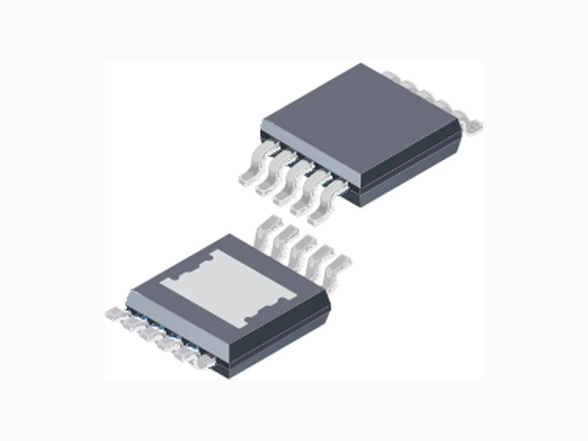
- Home Audio Network and Telecom Typical Application Diagram Typical application schematic, configured for VIN = 5 V , VOUT = 1.8 V, IOUT = 2.0 A at 2 MHz CIN2 0.1 µF 0805 CIN3 10 nF 0603 CO2 10 µF 1206 CO3 0.1 µF 0805 CO4 10 nF 0603A8650 SS8 EN/SYNC3 FSET5 VIN10 GND9 POK 4 FB 7 COMP6 PGND2 SW 1 VOUT RFB2 7.15 kΩ RFB1 9.09 kΩ CSS 10 nF CIN1 3.3 µF 1206 RFSET 10.7 kΩ VIN EN/SYNC POK RZ 6.65 kΩCP 22 pF CZ 1.5 nF LO 1.0 µH RPU 10 kΩ CO1 10 µF 1206 3.3V 10-pin MSOP with exposed thermal pad (suffix LY) 10-pin DFN with exposed thermal pad (suffix EJ) Features and Benefits
Low Input Voltage, Adjustable Frequency A Synchronous Buck Regulator with EN/SYNC and Power OKA8650 Allegro MicroSystems, LLC
115 Northeast Cutoff
Worcester, Massachusetts 01615-0036 U.S.A. Absolute Maximum Ratings1 Characteristic Symbol Notes Rating Unit VIN Pin to GND VIN –0.3 to 6 V SW to GND2 VSW Continuous –0.3 to VIN + 0.3 V t < 50 ns –1.0, VIN + 2.0 V All other pins –0.3 to 6.0 V Operating Ambient Temperature TA K temperature range –40 to 125 ºC Maximum Junction Temperature TJ(max) 150 ºC Storage Temperature Tstg –55 to 150 ºC 1Operation at levels beyond the ratings listed in this table may cause permanent damage to the device. The Absolute Maximum ratings are stress ratings only, and functional operation of the device at these or any other conditions beyond those indicated in the Electrical Characteristics table is not implied. Exposure to Absolute Maximum-rated conditions for extended periods may affect device reliability. 2SW has internal clamp diodes to GND and VIN . Applications that forward bias these diodes should take care not to exceed the IC package power dissipation limits. (UVLO), cycle-by-cycle overcurrent protection (OCP), hiccup mode short circuit protection (HIC), overvoltage protection (OVP), and thermal shutdown (TSD). In addition, the A8650 provides open circuit, adjacent pin short circuit, and short to ground protection at every pin to satisfy the most demanding automotive applications. The A8650 is available in both 10-pin MSOP and DFN packages with an exposed pad for enhanced thermal dissipation. It is lead (Pb) free, with 100% matte tin leadframe plating.
- Stable with ceramic output capacitors
- Enable input, and Power OK (POK) output
- Cycle-by-cycle current limiting (OCP)
- Hiccup mode short circuit protection (HIC)
- Overvoltage protection (OVP)
- Overtemperature protection (TSD)
- Open circuit and adjacent pin short circuit tolerant
- Short to ground tolerant at every pin Features and Benefits (continued) Description (continued) Thermal Characteristics may require derating at maximum conditions, see application information Characteristic Symbol Test Conditions* Value Unit Package Thermal Resistance (LY) R θJA On 4-layer PCB based on JEDEC standard 48 ºC/W Package Thermal Resistance (EJ) R θJA On 4-layer PCB based on JEDEC standard 45 ºC/W *Additional thermal information available on the Allegro website. Selection Guide Part Number Operating Ambient Temperature Range TA, (°C) Package Packing Leadframe Plating A8650KLYTR-T –40 to 125 10-pin MSOP with exposed thermal pad 4000 pieces per 13-in. reel 100% matte tin A8650KEJTR-T -40 to 125 10-pin DFN with exposed thermal pad 1500 pieces per 7-in reel 100% matte tin Specifications
Low Input Voltage, Adjustable Frequency A Synchronous Buck Regulator with EN/SYNC and Power OKA8650 Allegro MicroSystems, LLC Worcester, Massachusetts 01615-0036 U.S.A. Table of Contents Specifications 2 Functional Block Diagram Pin-out Diagram and Terminal List 5 Characteristic Performance Functional Description Overview 11 Reference Voltage 11 Oscillator/Switching Frequency 11 Transconductance Error Amplifier 11 Slope Compensation 11 Sleep Mode 12 Enable/Synchronization (EN/SYNC) Input 12 Power MOSFETs 12 Pulse Width Modulation (PWM) 13 Current Sense Amplifier 13 Soft Start (Startup) and Inrush Current Control 13 Pre-Biased Startup 13 Power OK (POK) Output 14 Protection Features 14 Undervoltage Lockout (UVLO) 14 Thermal Shutdown (TSD) 14 Overvoltage Protection (OVP) 14 Cycle-by-Cycle Overcurrent Protection (OCP) 14 Output Short Circuit (Hiccup Mode) Protection 15
Application Information
Design and Component Selection 18 Setting the Output Voltage (VOUT, RFB1, RFB2) 18 Base PWM Switching Frequency (RFSET) 18 Output Inductor (LO) 19 Output Capacitors 20 Input Capacitors 21 Soft Start and Hiccup Mode Timing (CSS) 21 Compensation Components (RZ , CZ , CP ) 22 A Generalized Tuning Procedure 24 Power Dissipation and Thermal Calculations 25 PCB Component Placement and Routing 27 Package Outline Drawing 29
Low Input Voltage, Adjustable Frequency A Synchronous Buck Regulator with EN/SYNC and Power OKA8650 Allegro MicroSystems, LLC Worcester, Massachusetts 01615-0036 U.S.A. Functional Block Diagram 125 ns Regulators ON VIN 0.8V POR Off Off S R Q Q FAULT = 1, if: EN = 0 or UVLO = 1 EN/SYNC VREF HICCUP = 1 if: FB < 625 mV and COMP ≈ 1.25 V and
7 OCP events
tOFF(MIN) GND FAULT PWM_CLK CURRENT CURRENT FBOK Falling Delay Oscillator ADJ Slope ADJ Compensation Current Sense fOSC fSYNC VSSOFFS FBOK COMP CLAMP_ACTIVE CLAMP_ACTIVE VPWMOFFS POK Comparator OVP Comparator PAD Error Amplifier Digital Delay POK
7 PWM
92% x VREF 88% x VREF 115% x VREF 111% x VREF 10 ns VIN 1.5 kΩ 2 kΩ POR 200 mV VIN POR VIN 20 µA PWM Comparator 10 µA OFF Clamp 1.25 V FSET
1.65 V (typ)
1.25 V (typ)
0.8 V (max)
55 mΩ Protection EN_HICCUP VIN (UVLO) EN / CLR HICCUP LATCHED HIC RST (100 mV) CURRENT (OCP) OCP COUNT EN FB HICCUP 350 mV 70 mΩ HICCUP EN/SYNC > 1.2 x fOSC Non-Overlap FB OFF OFF 100 kΩ SW PGND 150 nA
Low Input Voltage, Adjustable Frequency A Synchronous Buck Regulator with EN/SYNC and Power OKA8650 Allegro MicroSystems, LLC Worcester, Massachusetts 01615-0036 U.S.A. Pin-out Diagrams and Terminal List Table Terminal List Table Number Name Function 1 SW The drain of both the internal high- and low-side MOSFETs. The output inductor (LO) should be connected to this pin. LO should be placed as close as possible to this pin and connected with relatively wide traces. 2 PGND Power ground connection.
3 EN/SYNC
Enable and synchronization input. This pin is a logic input that turns the regulator on or off: set this pin to logic high to turn the regulator on or set this pin to logic low to turn the regulator off. This pin also functions as a synchronization input to allow the PWM frequency to be set by an external clock. 4 POK Power OK output signal. This pin is an open drain output that transitions from low impedance to high impedance when the output is within the final regulation voltage. 5 FSET Frequency setting pin. A resistor, R FSET , from this pin to GND sets the PWM switching frequency . See figure 10 and/or equation 2 to determine the value of RFSET . 6 COMP Output of the error amplifier and compensation node for the current mode control loop. Connect a series RC network from this pin to GND for loop compensation. See the Design and Component Selection sections of this datasheet for further details. 7 FB Feedback (negative) input to the error amplifier. Connect a resistor divider from the regulator output node, VOUT, to this pin to program the output voltage. 8 SS Soft start pin. Connect a capacitor, C SS , from this pin to GND to set the soft start time. This capacitor also determines the hiccup period during overcurrent. 9 GND Ground connection. 10 VIN Power input for the control circuits and the source of the internal high-side P-channel MOSFET. Connect this pin to a power supply of 2.5 to 5.5 V. A high quality ceramic capacitor should be placed very close to this pin. 0 PAD Exposed pad of the package providing enhanced thermal dissipation. This pad must be connected to the ground plane(s) of the PCB with at least 6 vias, directly in the pad. SW PGND EN/SYNC POK FSET VIN GND SS FB COMP PAD FSET POK EN/SYNC PGND SW COMP FB SS GND VIN PAD Package LY, 10-Pin MSOP Pin-out Diagram Package EJ, 10-Pin DFN Pin-out Diagram XREF XREF
Low Input Voltage, Adjustable Frequency A Synchronous Buck Regulator with EN/SYNC and Power OKA8650 Allegro MicroSystems, LLC Worcester, Massachusetts 01615-0036 U.S.A. ELECTRICAL CHARACTERISTICS Valid at –40°C ≤ TA = TJ ≤ 125°C, VIN = 5 V; unless otherwise specified Characteristic Symbol Test Conditions Min. Typ. Max. Unit Input Voltage Specifications Operating Input Voltage Range VIN 2.5 − 5.5 V VIN UVLO Start Threshold VINUVSTART VIN rising 2.00 2.22 2.45 V VIN UVLO Stop Threshold VINUVSTOP VIN falling 1.80 2.02 2.25 V VIN UVLO Hysteresis VINUVHYS − 200 − mV Input Currents Input Quiescent Current I Q VEN/SYNC = 5 V, VFB = 1.0 V, no PWM switching − 2 4 mA Input Sleep Supply Current IQSLEEP VIN = VSW = 5 V, VEN/SYNC ≤ 0.4 V − 1 3 μA Reference Voltage Reference (Feedback) Voltage V REF 2.5 < VIN < 5.5 V, VFB = VCOMP 792 800 808 mV Error Amplifier Feedback Input Bias Current 1 IFB VCOMP = 0.7 V, VFB regulated so that ICOMP = 0 A – –150 –300 nA Open Loop V oltage Gain2 AVOL − 65 − dB Transconductance gm ICOMP = 0 μA, VSS > 500 mV 550 750 950 μA/V V < VSS < 500 mV – 250 – μA/V Source Current IEA(SRC) VFB < 0.8 V, VCOMP = 0.7 V − –50 − μA Sink Current IEA(SINK) VFB > 0.8 V, VCOMP = 0.7 V − +50 − μA Maximum Output V oltage VEAO(MAX) 1.00 1.25 1.50 V COMP Pull Down Resistance RCOMP FAULT = 1, HICCUP = 1, or EN/SYNC = low − 1.5 − kΩ Pulse Width Modulation (PWM) PWM Ramp Offset VPWMOFFS VCOMP for 0% duty cycle − 350 − mV High-Side MOSFET Minimum Controllable On-Time tON(MIN) − 65 105 ns Low-Side MOSFET Minimum On Time tOFF(MIN) Does not include total gate driver non-overlap time, 2 x t NO − 50 100 ns Gate Driver Non-Overlap Time2 tNO − 15 − ns COMP to SW Current Gain gmPOWER − 4.5 − A/V Slope Compensation2 SE fsw = 2.0 MHz 1.65 2.35 2.85 A/μs fsw = 0.25 MHz 0.21 0.29 0.36 A/μs MOSFET Parameters High-Side MOSFET On-Resistance3 RDS(ON)HS TA = 25°C, IDS = 100 mA − 70 80 mΩ IDS = 100 mA − − 145 mΩ SW Node Rise Time2 tR(SW) VIN = 5 V − 12 − ns High-Side MOSFET Leakage4 ILKG(HS) VEN/SYNC ≤ 0.4 V, VSW = 0 V, VIN = 5 V, –40˚C < TA = TJ < 85˚C − − 4 μA TA = TJ = 125˚C − 5 25 μA Continued on the next page…
Low Input Voltage, Adjustable Frequency A Synchronous Buck Regulator with EN/SYNC and Power OKA8650 Allegro MicroSystems, LLC Worcester, Massachusetts 01615-0036 U.S.A. MOSFET Parameters (continued) Low-Side MOSFET On-Resistance3 RDS(on)LS TA = 25°C, IDS = 100 mA − 55 65 mΩ IDS = 100 mA − − 115 mΩ Low-Side MOSFET Leakage4 ILKG(LS) VEN/SYNC ≤ 0.4 V, VSW = 5 V, VEN/SYNC ≤ 0.4 V, VSW = 5 V, TA = TJ = 125˚C − 4 10 μA Oscillator Frequency Oscillator Frequency fOSC RFSET = 8.45 kΩ 2.20 2.45 2.70 MHz RFSET = 23.2 kΩ 0.90 1.00 1.10 MHz RFSET = 100 kΩ − 250 − kHz Synchronization Timing Synchronization Frequency Range f SW(MULT) Relative to fOSC(typ) 1.2 x fOSC − 1.5 x fOSC – Synchronized PWM Frequency fSYNC − − 2.9 MHz Synchronization Input Duty Cycle D SYNC − − 80 % Synchronization Input Pulse Width t PWSYNC VIN = 3.3 V, VEN/SYNC = 3.3 V pulse input 200 − − ns Synchronization Input Edge Rise Time2 trSYNC − 10 15 ns Synchronization Input Edge Fall Time2 tfSYNC − 10 15 ns Enable/Synchronization Input EN/SYNC High Threshold V EN/SYNC(H) VEN/SYNC rising − − 1.8 V EN/SYNC Low Threshold VEN/SYNC(L) VEN/SYNC falling 0.8 − − V EN/SYNC Hysteresis VEN/SYNC (HYS) VEN/SYNC(H) – VEN/SYNC(L) − 200 − mV EN/SYNC Digital Delay tSLEEP VEN/SYNC transitioning low − 32 − PWM cycles EN/SYNC Input Resistance REN/SYNC 50 100 − kΩ EN/SYNC Pulse Rejection tEN/SYNCR VIN = 3.3 V, VEN/SYNC = 1.3 V pulse input − 10 − ns Overcurrent Protection (OCP) and Hiccup Mode Pulse-by-Pulse Current Limit ILIM(5%) Duty Cycle = 5% 3.5 4.1 4.7 A ILIM(90%) Duty Cycle = 90% 2.3 3.1 4.2 A Hiccup Disable Threshold HICDIS VFB rising − 750 − mV Hiccup Enable Threshold HICEN VFB falling − 625 − mV OCP / HICCUP Count Limit OCPLIMIT Hiccup enabled, OCP pulses − 7 − counts ELECTRICAL CHARACTERISTICS (Continued) Valid at –40°C ≤ TA = TJ ≤ 125°C, VIN = 5 V; unless otherwise specified Characteristic Symbol Test Conditions Min. Typ. Max. Unit Continued on the next page…
Low Input Voltage, Adjustable Frequency A Synchronous Buck Regulator with EN/SYNC and Power OKA8650 Allegro MicroSystems, LLC Worcester, Massachusetts 01615-0036 U.S.A. Soft Start (SS Pin) SS Offset Voltage VSSOFFS VSS rising due to ISSSU 120 200 270 mV SS Fault/Hiccup Reset Voltage VSS_RESET VSS falling due to ISSHIC − 100 120 mV SS Startup (Source) Current ISSSU VSS = 1 V, HICCUP = FAULT = 0 −10 –20 −30 μA SS Hiccup (Sink) Current ISSHIC VSS = 0.5 V, HICCUP = 1 5 10 20 μA SS Input Resistance RSS FAULT = 1 or EN/SYNC = low − 2 − KΩ SS to VOUT Delay Time tSS(DELAY) CSS = 22 nF − 175 − μs VOUT Soft Start Ramp Time tSS CSS = 22 nF − 880 − μs SS Switching Frequency fSW(SS) VFB = 0 V − fSW / 3 − − VFB ≥ 600 mV − fSW − − Power OK (POK Pin) Output POK Output Voltage V POK IPOK = 4 mA − − 0.4 V POK Undervoltage Threshold POKUV VFB rising, as a percent of VREF 89 92 95 % POK Undervoltage Hysteresis POK UVHYS VFB falling, as a percent of VREF − 4 − % POK Overvoltage Threshold POKOV VFB rising, as a percent of VREF 112 115 118 % POK Overvoltage Hysteresis POKOVHYS VFB falling, as a percent of VREF − 4 − % POK Digital Delay POKDLY VFB rising only − 7 − PWM cycles POK Leakage IPOK(LKG) VPOK = 5 V, VCOMP ≤ 0.3 V − − 1 μA Thermal Shutdown Protection (TSD) Thermal Shutdown Threshold
2 TTSD Temperature rising 155 170 185 ºC
Thermal Shutdown Hysteresis2 TTSDHYS Temperature falling − 20 − ºC 1For input and output current specifications, negative current is defined as coming out of the node or pin (sourcing), positive current is defined as going into the node or pin (sinking). 2Ensured by design and characterization, not production tested. 3TA = TJ = 25˚C ensured by design and characterization, not production tested. 4TA = TJ = 85˚C ensured by design and characterization, not production tested. ELECTRICAL CHARACTERISTICS (Continued) Valid at –40°C ≤ TA = TJ ≤ 125°C, VIN = 5 V; unless otherwise specified Characteristic Symbol Test Conditions Min. Typ. Max. Unit
Low Input Voltage, Adjustable Frequency A Synchronous Buck Regulator with EN/SYNC and Power OKA8650 Allegro MicroSystems, LLC Worcester, Massachusetts 01615-0036 U.S.A. Characteristic Performance 792 794 796 798 800 802 804 806 808 -50 -25 0 25 50 75 100 125 150 VREF (mV) Temperature (°C) 0.75 1.00 1.25 1.50 1.75 2.00 2.25 2.50 2.75 -50 -25 0 25 50 75 100 125 150 fOSC (MHz) Temperature (°C) f OSC = 2.44 MHz f OSC = 1.00 MHz 1.70 1.80 1.90 2.00 2.10 2.20 2.30 2.40 2.50 -50 -25 0 25 50 75 100 125 150 VIN (V) Temperature (°C) Start, VINUVSTART Stop, VINUVSTOP 100 105 110 115 120 -50 -25 0 25 50 75 100 125 150 Threshold (% of VFB) Temperature (°C) POKOV, V FB rising POKOV, V FB falling POKUV, V FB rising POKUV, V FB falling 3.5 3.6 3.7 3.8 3.9 4.0 4.1 4.2 4.3 4.4 4.5 -50 -25 0 25 50 75 100 125 150 ILIM (5%) (A) Temperature (°C) 550 600 650 700 750 800 850 900 950 -50 -25 0 25 50 75 100 125 150 EA gm (µA/V) Temperature (°C) Reference Voltage versus Temperature Switching Frequency versus Temperature VIN UVLO Start and Stop Thresholds versus Temperature POKOV and POKUV Thresholds versus Temperature Error Amplifier Transconductance versus Temperature Cycle-by-Cycle Current Limit at tON(MIN) versus Temperature
Low Input Voltage, Adjustable Frequency A Synchronous Buck Regulator with EN/SYNC and Power OKA8650 Allegro MicroSystems, LLC Worcester, Massachusetts 01615-0036 U.S.A. 1.0 1.1 1.2 1.3 1.4 1.5 1.6 1.7 1.8 -50 -25 0 25 50 75 100 125 150 EN/SYNC (V) Temperature (°C) VEN/SYNC(L) VEN/SYNC(H) -50 -25 0 25 50 75 100 125 150 SS Pin Cu rrent (µA) Temperature (°C) Startup, ISSSU Hiccup, ISSHIC 0.00 0.05 0.10 0.15 0.20 0.25 0.30 0.35 0.40 -50 -25 0 25 50 75 100 125 150 VPOK (V) Temperature (°C) VPOK at 4 mA 550 575 600 625 650 675 700 725 750 775 800 825 850 -50 -25 0 25 50 75 100 125 150 Threshold (mV) Temperature (°C) HICEN, V FB falling HICDIS, V FB rising 0.0 0.5 1.0 1.5 2.0 2.5 3.0 3.5 4.0 -50 -25 0 25 50 75 100 125 150 IQSLEEP (µA) Temperature (°C) 0.0 2.5 5.0 7.5 10.0 12.5 15.0 17.5 20.0 -50 -25 0 25 50 75 100 125 150 Leakage Cu rrent (µA) Temperature (°C) High-Side, ILKG(HS) Low-Side, ILKG(LS) EN/SYNC High and Low Thresholds VIN Sleep Current versus Temperature Hiccup Enable and Disable Thresholds versus Temperature POK Low Output Voltage versus Temperature versus Temperature High- and Low-Side MOSFETs Leakage Currents versus Temperature Soft Start Startup and Hiccup versus Temperature
Worcester, Massachusetts 01615-0036 U.S.A. sation, and excellent stability. ground short circuit protection. from VOUT to the FB pin of the A8650. typical application schematic, sets the base switching frequency. provided in the Component Selection section of this datasheet. reference, whichever is lower. sation network to roll-off the loop gain at higher frequencies. Figure 1. A8650 Error Amplifier
Worcester, Massachusetts 01615-0036 U.S.A. Figure 3. External circuit for automatically enabling the A8650 from VIN Figure 2. PWM switching stops 32 PWM cycles after EN/SYNC transitions
32 PWM
Worcester, Massachusetts 01615-0036 U.S.A. impedance by turning off both the upper and lower MOSFETs. the comparator is connected to the output of the error amplifier. plete soft start operation is shown in figure 4. Figure 4. Startup to VOUT = 1.8 V, at IOUT = 2.0 A with C SS = 10 nF
Worcester, Massachusetts 01615-0036 U.S.A.
- V FB is rising, and is < 92% of the internal reference voltage, or
- VFB is rising, and is > 115% of the internal reference voltage, or
- EN/SYNC is low for more than 32 PWM clock cycles, or
- VIN pin UVLO occurs, or
- Thermal Shutdown (TSD) occurs. If the A8650 is running and EN/SYNC transitions low for more than 32 PWM clock cycles, then POK will transition low and remain low only as long as the internal circuitry is able to enhance the open-drain output device. When V IN fully collapses, POK will return to the high impedance state. The POK compara- tor incorporates hysteresis to prevent chattering due to voltage ripple at the FB pin. Protection Features Undervoltage Lockout (UVLO) An undervoltage lockout (UVLO) comparator monitors the volt- age at the VIN pin and keeps the regulator disabled if the voltage is below the lockout threshold (V INUVSTART). The UVLO com- parator incorporates enough hysteresis (VINUVHYS ) to prevent on/off cycling of the regulator due to IR drops in the VIN path during heavy loading or during startup. Figure 8 shows the A8650 operation for a UVLO-initiated startup (EN/SYNC = high, V IN ramps up). Thermal Shutdown (TSD) The A8650 protects itself from overheating by means of an internal thermal monitoring circuit. If the junction temperature exceeds the thermal shutdown threshold (T TSD , 170°C (typ)) the voltages at the soft start and COMP pins will be pulled to GND and both the high-side and low-side MOSFETs will be turned off. The A8650 will automatically restart when the junction temperature decreases more than the thermal shutdown hysteresis TSDHYS , 20°C(typ)). Figure 8 shows the A8650 operation dur- ing and after a TSD event. Overvoltage Protection (OVP) The A8650 uses the FB pin to provide a basic level of overvolt- age protection. An overvoltage condition could occur if the load current decreases very quickly or the regulator output is pulled high by some external voltage. When an overvoltage condition is detected, POK is pulled low and PWM switching stops. The COMP and soft start pins are not directly affected by OVP. If the regulator output decreases back to the allowed operating range, POK will transition to high and PWM switching will resume. Cycle-by-Cycle Overcurrent Protection (OCP) The A8650 monitors the current in the high-side MOSFET and if the current exceeds the cycle-by-cycle overcurrent threshold LIM ) then the high-side MOSFET is turned off. Normal PWM operation resumes on the next clock pulse from the oscillator. The A8650 includes leading edge blanking to prevent falsely trigger- ing the cycle-by-cycle current limit when the upper MOSFET is turned on. Because of the addition of the slope compensation ramp to the inductor current, the A8650 delivers more current at lower duty cycles and less current at higher duty cycles. For a given duty cycle, this results in a little more current being available at lower switching frequencies than at higher frequencies.
Figure 5. Startup to VOUT = 1.8 V, VOUT pre-biased to 0.9 V
Worcester, Massachusetts 01615-0036 U.S.A. DIS , 750 mV(typ)) hiccup mode protection is disabled. level. Hiccup mode operation is shown in both figures 7 and 8. Figure 6. Cycle-by-cycle current limiting versus duty cycle; at Figure 7. Hiccup mode operation and recovery
Worcester, Massachusetts 01615-0036 U.S.A. TABLE 1. Summary of A8650 Fault Modes and Operation
32 PWM cycles
Worcester, Massachusetts 01615-0036 U.S.A. Figure 8. A8650 timing diagram
Low Input Voltage, Adjustable Frequency A Synchronous Buck Regulator with EN/SYNC and Power OKA8650 Allegro MicroSystems, LLC Worcester, Massachusetts 01615-0036 U.S.A. Design and Component Selection Setting the Output Voltage (VOUT, RFB1, RFB2) The output voltage of the A8650 is determined by connecting a resistor divider from the output node (VOUT) to the FB pin as shown in figure 9. There are trade-offs when choosing the value of the feedback resistors. If the series combination (R FB1+RFB2) is relatively low, then the light-load efficiency of the regula- tor will be reduced. So, to maximize that efficiency, it is best to choose high-value resistors. On the other hand, if the parallel combination (R FB1 // RFB2 ) is too high, then the regulator may be susceptible to noise coupling into the FB pin. In general, to produce the target output voltage, VOUT : = – 10.8 (V) VOUT RFB2 RFB1 (1) T able 2 shows the most common output voltages and recom- mended feedback resistors, assuming < 0.2% ef ficiency loss at light load of 100 mA, and a parallel combination of 4 kΩ presented to the FB pin. For optimal system accuracy , it is recom- mended that the feedback resistors have ≤1% tolerances. Base PWM Switching Frequency (RFSET) The base PWM switching frequency is set by connecting a resis- tor from the FSET pin to ground. Figure 10 is a graph showing the relationship between the typical switching frequency (y-axis) and the FSET resistor (x-axis). For a particular base switching Figure 9. Connecting a feedback resistor divider Table 2. Recommended Feedback Resistor Values Figure 10. PWM switching frequency versus RFSET
Low Input Voltage, Adjustable Frequency A Synchronous Buck Regulator with EN/SYNC and Power OKA8650 Allegro MicroSystems, LLC Worcester, Massachusetts 01615-0036 U.S.A. frequency (fOSC ), the FSET resistor can be calculated as follows: = – 1.7fOSC 24900RFSET (2) where fOSC is in kHz and RFSET is in kΩ. The oscillator frequency will be the final output switching fre- quency (unless the synchronization function is applied), so when the oscillator frequency is being chosen, the designer should be aware of the minimum controllable on-time, t ON(MIN) , of the A8650. If the system required on-time is less than the A8650 minimum controllable on-time, then switch node jitter will occur and the output voltage will have increased ripple or oscillations. The minimum oscillator frequency required should be calculated as follows: = tON(MIN) ×VIN(MAX) VOUTfSWMAX (3) where VOUT is the output voltage, tON(MIN) is the minimum controllable on-time of the A8650 (worst case 105 ns), and VIN(MAX) is the maximum required operational input voltage (not the peak surge voltage). If the A8650 PWM synchronization function is employed, then the oscillator frequency should be chosen such that jitter will not result at the maximum synchronized switching frequency, deter- mined from equation 3: 1.5 × fSW < fSWMAX (4) Output Inductor (LO) When considering a peak current mode regulator, it is common knowledge that, without adequate slope compensation, the system will become unstable when the duty cycle is near or above 50%. However, the slope compensation in the A8650 is a fixed value E ). Therefore, it is important to calculate an inductor value so the falling slope of the inductor current (SF) will work well with the A8650 slope compensation. Equations 5 and 6 can be used to calculate a range of values for the output inductor based on the well known approach of provid- ing slope compensation that matches 50% to 100% of the falling slope of the inductor current: ≤ ≤LO2 × SE VOUT SE VOUT (5) where LO is in µH. In equation 5, the slope compensation (SE ) is a function of switching frequency, as follows: SE = 1.175 × f OSC (6) where SE is in A/µs and fSW is in MHz. More recently, Dr. Raymond Ridley presented a formula to calcu- late the amount of slope compensation required to critically damp the double poles at half the PWM switching frequency: SE LO ≥ VIN(min)VOUT VOUT 1–0.18 × (7) This formula allows the inclusion of the duty cycle (D), which should be calculated at the minimum input voltage to ensure optimal stability . Also, to avoid dropout (that is, saturation of the buck regulator), VIN(min) must be approximately 0.75 to 1.0 V above VOUT when calculating the inductor value with equation 7. If equations 6 or 7 yield an inductor value that is not a standard value, then the next closest available value should be used. The final inductor value should allow for 10% to 20% of initial toler- ance and 10% to 20% of inductor saturation. The saturation current of the inductor should be higher than the peak current capability of the A8650. Ideally, for output short circuit conditions, the inductor should not saturate even at the highest cycle-by-cycle current limit at minimum duty cycle LIM(5%) ; 4.7 A(max)). This may be too costly. At the very least, the inductor should not saturate given the peak operating current according to the following equation: =IPEAK 4.1 – SE × (VOUT ) 1.15 × fSW × VIN(max) (8) where VIN(max) is the maximum continuous input voltage, such as 5.5 V .
Low Input Voltage, Adjustable Frequency A Synchronous Buck Regulator with EN/SYNC and Power OKA8650 Allegro MicroSystems, LLC Worcester, Massachusetts 01615-0036 U.S.A. Starting with equation 8, and subtracting half of the inductor ripple current, provides us with an interesting equation to predict the typical DC load capability of the regulator at a given duty cycle (D): =IOUT(DC) 4.1 – SE× D fSW 2 × fSW × LO VOUT × (1– D) (9) where D is VOUT / VIN. After an inductor is chosen, it should be tested during output short circuit conditions. The inductor current should be monitored using a current probe. A good design would ensure neither the inductor nor the regulator are damaged when the output is shorted to ground at maximum input voltage and the highest expected ambient temperature. Output Capacitors The output capacitors filter the output voltage to provide an acceptable level of ripple voltage and they store energy to help maintain voltage regulation during a load transient. The voltage rating of the output capacitors must support the output voltage with sufficient design margin. The output voltage ripple (ΔVOUT ) is a function of the output capacitor parameters: COUT , ESRCOUT , and ESLCOUT: =∆VOUT ∆IL × ESRCOUT ∆IL × ESLCOUT VIN–VOUT LO 8 fSWCOUT (10) The type of output capacitors will determine which terms of equation 10 are dominant. For ceramic output capacitors the ESR COUT and ESLCOUT are virtually zero, so the output voltage ripple will be dominated by the third term of equation 10: =∆VOUT ∆IL 8 fSWCOUT (1 1) To reduce the voltage ripple of a design using ceramic output capacitors, simply: increase the total capacitance, reduce the inductor current ripple (that is, increase the inductor value), or increase the switching frequency. For electrolytic output capacitors the value of capacitance will be relatively high, so the third term in equation 10 will be very small. The output voltage ripple will be determined primarily by the first two terms of equation 10: =∆VOUT ∆IL × ESRCOUT × ESLCOUT VIN – VOUT LO + (12) T o reduce the voltage ripple of a design using electrolytic output capacitors, simply: decrease the equivalent ESRCOUT and ESLCOUT by using a high(er) quality capacitor, or add more capacitors in parallel, or reduce the inductor current ripple (that is, increase the inductor value). The ESR of some electrolytic capacitors can be quite high so we recommend choosing a quality capacitor that clearly documents the ESR or the total impedance in the data sheet. Also, the ESR of electrolytic capacitors usually increases significantly at cold ambients, as much as 10×, which increases the output voltage ripple and, in most cases, significantly reduces the stability of the system. The transient response of the regulator depends on the number and type of output capacitors. In general, minimizing the ESR of the output capacitance will result in a better transient response. The ESR can be minimized by simply adding more capacitors in parallel or by using higher quality capacitors. At the instant of a fast load transient (di/dt), the output voltage will change by the amount = × +∆VOUT ∆ILOAD di dt ESLCOUTESRCOUT (13) After the load transient occurs, the output voltage will deviate from its nominal value for a short time. This time will depend on the system bandwidth, the output inductor value, and output capacitance. Eventually, the error amplifier will bring the output voltage back to its nominal value. The speed at which the error amplifier will bring the output volt- age back to its setpoint will depend mainly on the closed-loop bandwidth of the system. A higher bandwidth usually results in a shorter time to return to the nominal voltage. However, a higher bandwidth system may be more difficult to obtain acceptable gain and phase margins. Selection of the compensation components Z, CZ, CP ) are discussed in more detail in the Compensation Components section of this datasheet.
Worcester, Massachusetts 01615-0036 U.S.A. mended), and fSW is the nominal PWM output frequency. stability versus both DC bias and temperature. Figure 11. Input capacitor ripple versus duty cycle
Worcester, Massachusetts 01615-0036 U.S.A. figure 12. This phenomena is more pronounced when using high values of ICO ensure that hiccup mode is not falsely triggered. bandwidth, and optimize the transient response. the RZ resistor (discussed and identified later as fP3).
Worcester, Massachusetts 01615-0036 U.S.A. half the switching frequency. error amplifier (gm), and the compensation network RZ CZ CP . RO is the error amplifier output impedance (AVOL/gm ). slow transient recovery time, as will be shown later.
1 MHz
Figure 13. Control-to-Output Bode plot Figure 14. Type-II compensated error amplifier Bode plot
Worcester, Massachusetts 01615-0036 U.S.A. design considerations provided above.
- Choose the system bandwidth (fC ). This is the frequency at
generally makes it easier to obtain higher gain and phase margins.
- Determine the frequency of the pole (fP1). This pole is formed
- Calculate a range of values for the CZ capacitor. Use the fol-
Figure 15. Bode plot of the complete system (red curve) Figure 16. Transient recovery comparison for fZ2 at 16 kHz / 73° and
Low Input Voltage, Adjustable Frequency A Synchronous Buck Regulator with EN/SYNC and Power OKA8650 Allegro MicroSystems, LLC Worcester, Massachusetts 01615-0036 U.S.A. 5. Calculate the frequency of the ESR zero (fZ1) formed by the output capacitor(s). Use equation 23 (repeated here): =fZ1 COUTESR× ×2 If fZ1 is at least one decade higher than the target crossover frequency (fC) then fZ1 can be ignored. This is usually the case for a design using ceramic output capacitors. Use equation 27 to calculate the value of CP by setting fP3 to either 5 × fC or fSW / 2, whichever is higher Alternatively, if fZ1 is near or below the target crossover fre- quency (fC), then use equation 27 to calculate the value of CP by setting fP3 equal to fZ1. This is usually the case for a design using high ESR electrolytic output capacitors. Power Dissipation and Thermal Calculations The power dissipated in the A8650 is the sum of the power dis- sipated from the VIN supply current (P IN), the power dissipated due to the switching of the internal power high-side MOSFET SW1 ), the power dissipated due to the rms current being conducted by the high- and low-side MOSFETs (PCOND1 and PCOND2), the power dissipated by the low-side MOSFET body diode during the non-overlap times, and the power dissipated by the internal gate drivers (P DRIVER1 and PDRIVER2). The power dissipated from the VIN supply current can be calcu- lated using the following equation: P IN = VIN × IQ + (VIN – VGS ) × (QG1 + QG2 ) × fSW (30) where VIN is the input voltage, IQ is the input quiescent current drawn by the A8650 (nominally mA), VGS is the MOSFET gate drive voltage, typically 5.0 V , QG1 and QG2 are the internal high- and low-side MOSFET gate charges (approximately 3.3 nC and 1.4 nC respectively), and fSW is the PWM switching frequency. The switching losses dissipated by the internal high-side MOSFET during PWM switching can be calculated using the following equation: =PSW1 VIN IOUT fSW(tr + tf )× × × (31) where VIN is the input voltage, IOUT is the output current, fSW is the PWM switching frequency, and tr and tf are the rise and fall times measured at the SW node. Approximate values for tr range from 10 to 15 ns. The fall time is usually about 50% faster than the rise time. The conduction losses dissipated by the high-side MOSFET while it is conducting can be calculated using the following equation: =PCOND1 Irms(FET) RDS(on)HS VOUT VIN × + 12 ∆IL IOUT = RDS(on)HS× (32) where IOUT is the regulator output current, ΔIL is the peak-to-peak inductor ripple current, and RDS(on)HS is the on-resistance of the high-side MOSFET. The conduction losses dissipated by the low-side MOSFET while it is conducting can be calculated using the following equation: =PCOND2 Irms(FET) RDS(on)LS VOUT VIN × +– 12 ∆IL IOUT1 2 = RDS(on)LS× (33) where IOUT is the regulator output current, ΔIL is the peak-to-peak inductor ripple current, and RDS(on)LS is the on-resistance of the low-side MOSFET. The RDS(on)of the MOSFETs has some initial tolerance plus an increase from self-heating and elevated ambient temperatures. A conservative design should accommodate an RDS(on) with at least a 15% initial tolerance plus 0.39%/°C increase due to temperature.
Low Input Voltage, Adjustable Frequency A Synchronous Buck Regulator with EN/SYNC and Power OKA8650 Allegro MicroSystems, LLC Worcester, Massachusetts 01615-0036 U.S.A. The power dissipated by the low-side MOSFET body diode dur- ing the non-overlap time can be calculated as follows: PNO = VSD × IOUT × 2 × t NO × fSW (34) where VSD is the source-to-drain voltage of the low-side MOSFET (typically 0.60 V), and tNO is the non-overlap time (15 ns (typ)). The power dissipated by the internal gate drivers can be calcu- lated using the following equation: PDRIVERS = (QG1 + QG2 ) × VGS × fSW (35) where QG1 and QG2 are the internal gate charges to drive the high- and low-side MOSFETs to VGS (approximately 3.3 nC and 1.4 nC at V , respectively), and fSW is the PWM switching frequency. Finally, the total power dissipated by the A8650 (PTOTAL) is the sum of the previous equations: PTOTAL = PIN + PSW1 + PCOND1 + PCOND2 + PNO + PDRIVERS (36) The average junction temperature can be calculated with the fol- lowing equation: TJ = PTOTAL × RθJA + TA (37) where PTOTAL is the total power dissipated as described in equation 36, RθJA is the junction-to-ambient thermal resistance (48°C/W on a 4-layer PCB), and TA is the ambient temperature. The maximum junction temperature will be dependent on how efficiently heat can be transferred from the PCB to ambient air. It is critical that the thermal pad on the bottom of the IC should be connected to a at least one ground plane using multiple vias. As with any regulator, there are limits to the amount of heat that can be dissipated before risking thermal shutdown. There are trade-offs between: ambient operating temperature, input voltage, output voltage, output current, switching frequency, PCB thermal resistance, airflow, and other nearby heat sources. Even a small amount of airflow will reduce the junction tempera- ture considerably.
Low Input Voltage, Adjustable Frequency A Synchronous Buck Regulator with EN/SYNC and Power OKA8650 Allegro MicroSystems, LLC Worcester, Massachusetts 01615-0036 U.S.A. PCB Component Placement and Routing A good PCB layout is critical if the A8650 is to provide clean, stable output voltages. Follow these guidelines to ensure a good PCB layout. Figure 17 shows a typical synchronous buck regula- tor schematic with the critical power paths/loops. Figure 18 shows an example PCB component placement and routing with the same critical power paths/loops as shown in the schematic. 1. Place the ceramic input capacitors as close as possible to the VIN pin and ground the capacitors at the PGND pin. The ceramic input capacitors and the A8650 must be on the same layer. Connect the input capacitors, the VIN pin, and the PGND pin with a wide trace. This critical loop is shown as trace 1 in figures and 18. 2. Place the output inductor (LO) as close as possible to the SW pin. The output inductor and the A8650 must be on the same layer. Connect the SW pin to the output inductor with a relatively wide trace or polygon. For EMI/EMC reasons, its best to mini- mize the area of this trace/polygon. This critical trace is shown as trace 2 in figure 17. Also, keep low-level analog signals (like FB and COMP) away from the SW metal. 3. Place the output capacitors relatively close to the output inductor and the A8650. Ideally, the output capacitors, output inductor and the A8650 should be on the same layer. Connect the output inductor and the output capacitors with a fairly wide trace. The output capacitors must use a ground plane to make a very low-inductance connection back to the PGND pin. These critical connections are shown as trace 3 in figures and 18. 4. Place the feedback resistor divider (RFB1 and RFB2) very close to the FB pin. Orient RFB2 such that the ground side is as close as possible to the A8650. 5. Place the compensation components (RZ , CZ , and CP ) as close as possible to the COMP pin. Orient CZ and CP such that their ground connections are as close as possible to the A8650. 6. Place and ground the FSET resistor as close as possible to the FSET pin. 7. The output voltage sense trace (from VOUT to R FB1 ) should be connected as close as possible to the load to obtain the best load regulation. 8. The thermal pad under the IC should be connected to a ground plane (preferably on the top and bottom layers) with as many vias as possible. Allegro recommends vias with an approximately 0.25 to 0.30 mm hole and a 0.13 to 0.18 mm ring. 9. Place the soft start capacitor (CSS ) as close as possible to the SS pin. Place a via to the GND plane as close as possible to this component. 10. When connecting the input and output ceramic capacitors to a power or ground plane, use multiple vias and place the vias as close as possible to the component pads. Do not use thermal reliefs (spokes) around the pads for the input and output ceramic capacitors. 11. EMI/EMC issues are always a concern. Allegro recommends having locations for an RC snubber from SW to ground. The snubber components can be placed on the back of the PCB and populated only if necessary. The resistor should be 0805 or 1206 size.
Worcester, Massachusetts 01615-0036 U.S.A. Figure 18. Example PCB component placement and routing Figure 17. Typical synchronous buck converter with critical paths/loops shown; a single-point ground is
Low Input Voltage, Adjustable Frequency A Synchronous Buck Regulator with EN/SYNC and Power OKA8650 Allegro MicroSystems, LLC Worcester, Massachusetts 01615-0036 U.S.A. Package LY, 10-Pin MSOP with Exposed Thermal Pad For Reference Only – Not for Tooling Use (Reference JEDEC MO-187) Dimensions in millimeters – NOT TO SCALE Dimensions exclusive of mold flash, gate burrs, and dambar protrusions Exact case and lead configuration at supplier discretion within limits shown A 0.86 ±0.05 SEATING PLANE 0.50 REF 0.25 2 1 2 1 A B 0.53 ±0.10 0.15 ±0.05 0.05 0.15 0° to 6°3.00 ±0.10 1.98 1.73 0.27 0.18 B Exposed thermal pad (bottom surface) Seating Plane Gauge Plane Terminal #1 mark area
Low Input Voltage, Adjustable Frequency A Synchronous Buck Regulator with EN/SYNC and Power OKA8650 Allegro MicroSystems, LLC Worcester, Massachusetts 01615-0036 U.S.A. Package EJ, 10-Pin DFN with Exposed Thermal Pad For Reference Only – Not for Tooling Use (Reference DWG 2860) Dimensions in millimeters –N OT TO SCALE Exact case and lead configuration at supplier discretion within limits shown A A B C B 1.64 2.38 0.30 0.50 0.85 3.10 CC0.08 11X C SEATING PLANE D 0.25+0.05 –0.07 0.05 0.00
2.38 NOM
1.65 NOM
0.5 BSC
0.2 REF
0.75 ±0.05 3.00 ±0.15 3.00 ±0.15 0.40 ±0.10 PCB Layout Reference View Terminal #1 mark area Exposed thermal pad (reference only, terminal #1 identifier appearance at supplier discretion) Reference land pattern layout (reference IPC7351 SON50P300X300X80-11WEED3M); all pads a minimum of 0.20 mm from all adjacent pads; adjust as necessary to meet application process requirements and PCB layout tolerances; when mounting on a multilayer PCB, thermal vias at the exposed thermal pad land can improve thermal dissipation (reference EIA/JEDEC Standard JESD51-5) Coplanarity includes exposed thermal pad and terminalsD
Low Input Voltage, Adjustable Frequency A Synchronous Buck Regulator with EN/SYNC and Power OKA8650 Allegro MicroSystems, LLC Worcester, Massachusetts 01615-0036 U.S.A.
Revision History
Revision Revision Date Description of Revision
6 January 13, 2014 Miscellaneous conforming edits
7 October 27, 2014 Revised equation 7
8 November 20, 2015 Added EJ 10-Pin DFN Package
For the latest version of this document, visit our website: www.allegromicro.com Copyright ©2015, Allegro MicroSystems, LLC Allegro MicroSystems, LLC reserves the right to make, from time to time, such departures from the detail specifications as may be required to permit improvements in the performance, reliability, or manufacturability of its products. Before placing an order, the user is cautioned to verify that the information being relied upon is current. Allegro’s products are not to be used in any devices or systems, including but not limited to life support devices or systems, in which a failure of Allegro’s product can reasonably be expected to cause bodily harm. The information included herein is believed to be accurate and reliable. However, Allegro MicroSystems, LLC assumes no responsibility for its use; nor for any infringement of patents or other rights of third parties which may result from its use.