
DATASHEET SEARCH SITE
Document overview
- Manufacturer or author: Provided By www.digicamel.com(FREE DATASHEET DOWNLOAD SITE)
- PDF pages: 52
Technical content
Description
Designed to provide the power supply requirements of next generation car audio and infotainment systems, the A8600 provides all the control and protection circuitry to produce four high current regulators, each with ±1.5% accuracy. The A8600 includes control circuitry to implement three adjustable, asynchronous buck regulators with integrated MOSFETs. Also, the A8600 provides the control circuitry, gate drivers, and current sensing to implement a synchronous buck controller with external MOSFETs. In standby mode, the A8600 draws less than 50 μA from V IN of 12 V while employing pulse frequency modulation (PFM) to deliver 3.3 V/40 μA via the always-on regulator, SW1. The always-on regulator operates down to at least V IN of 3.6 V (VIN falling). Features of the A8600 include: an EN/SYNC input to either turn the A8600 on/off or increase/decrease the base pulse width modulation (PWM) frequency, four adjustable soft-start times, and four external compensation pins. Output voltage monitoring of switchers SW2, SW3, and SW4 is provided by a single, open-drain POK output. In addition, the A8600 provides two high voltage, high-side switches with foldback overcurrent protection. These two high-side switches actively block reverse current. The A8600 also provides direct battery (BU) and switched (accessory) battery (ACC) detectors and a mute pulse output with an adjustable delay. A8600-DS, Rev. 3 Features and Benefits
- Four independent, high current switching regulators
- Adjustable 1.0 A/±1.5% always-on asynchronous buck regulator with an integrated 150 mΩ MOSFET (SW1) ▫ Employs PFM to deliver 3.3 V/40 μA while drawing less than 50 μA from V IN of 12 V ▫ Operates down to at least 3.6 VIN
- Adjustable 1.5 A/±1.5% asynchronous buck regulator with an integrated 120 mΩ high-side MOSFET (SW2)
- Adjustable 2.0 A/±1.5% asynchronous buck regulator with an integrated 110 mΩ MOSFET (SW3)
- Adjustable ±1.5% synchronous buck controller with integrated gate drivers and current sensing (SW4)
- Fixed 425 kHz, interleaved PWM switching frequency
- EN/SYNC input for PWM frequency scaling
- Adjustable soft-start time for each switching regulator
- All switching regulators provide prebias startup with zero reverse current
- All switching regulators have overvoltage protection
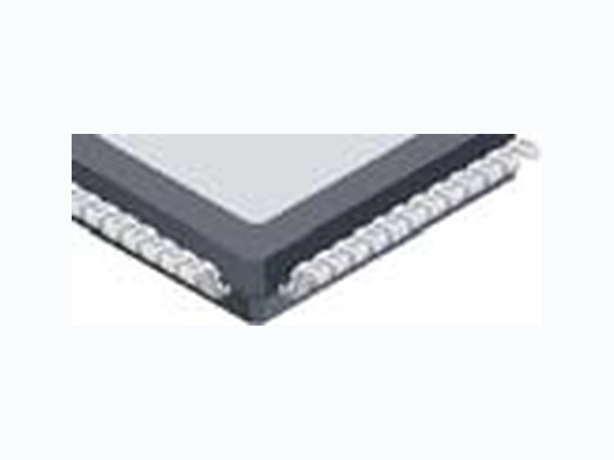
- External compensation for all switching regulators Quadruple Output Regulator with Two High-Side Switches, BU/ACC Voltage Detectors, and Mute Delay Package: 48-pin LQFP (suffix JP) Not to scale A8600 Switcher 1 (SW1) Always-On Adjustable Output Voltage Adjustable Output Voltage Adjustable Output Voltage Adjustable Output Voltage Adjustable ILIM PWM / PFM Asynchronous Buck Switcher 2 (SW2) PWM Switcher 3 (SW3) PWM Switcher 4 (SW4) PWM Regulator Asynchronous Buck Regulator Asynchronous Buck Regulator Synchronous Buck Controller BU and ACC Detectors Mute Pulse with Delay425 kHz 180° Shift (EN/SYNC) Charge Enable and Synchronization Pump High-Side Switch 2 (S2) High-Side Switch 1 (S1) 1.0 Ω Total with Foldback Limiting 1.0 Ω Total with Foldback Limiting Continued on the next page… Continued on the next page…
Figure 1. A8600 major features
Quadruple Output Regulator with Two High-Side Switches, BU/ACC Voltage Detectors, and Mute DelayA8600 2Allegro MicroSystems, Inc.
115 Northeast Cutoff
Worcester, Massachusetts 01615-0036 U.S.A. Protection features of the A8600 include pulse-by-pulse current limit, hiccup mode short circuit protection, asynchronous diode protection, BOOT voltage protection, undervoltage lockout, over- voltage protection and thermal shutdown. The A8600 is supplied in a low profile 48-pin LQFP package (suffix JP ) with exposed power pad. It is lead (Pb) free, with 100% matte- tin leadframe plating.
- Power OK (POK) open-drain output with de-glitch
- BU and ACC voltage detectors and comparators
- Mute control with programmable delay
- Two internal high-voltage, high-side NMOS switches (S1 and S2) with foldback short circuit protection
- High-side switches simultaneously controlled on/off
- High-side switches block reverse current
- Internal charge pump for high-side switch biasing
- Withstands surge voltages up to 40 V
- −40°C to 85°C ambient operating temperature range
- 150°C maximum junction temperature
- Thermally enhanced, surface mount package Features and Benefits (continued) Description (continued) Selection Guide Part Number Operating Ambient Temperature Range TA, (°C) Package Packing* Leadframe Plating A8600EJPTR-T –40 to 85 48-pin LQFP with exposed thermal pad 1500 pieces per 13-in. reel 100% Matte-Tin *Contact Allegro® for additional packing options.
Quadruple Output Regulator with Two High-Side Switches, BU/ACC Voltage Detectors, and Mute DelayA8600 3Allegro MicroSystems, Inc. Worcester, Massachusetts 01615-0036 U.S.A. Table of Contents Specifications 4 Absolute Maximum Ratings 4 Thermal Characteristics 4 Pin-out Diagram and List 5 Top Level Block Diagram 6 Typical Application Circuit 6 SW1/2/3 Detailed Block Diagram 7 SW4 Detailed Block Diagram 8 Electrical Characteristics Table 9 General Specifications 9 SW1 Regulator 10 SW2 Regulator 12 SW3 Regulator 14 SW4 Controller 16 S1, S2 Switches 18 BU and ACC Comparators 18 CTMR and MUTE 19 Timing Diagrams 20 SW1 Normal PWM Operation 20 SW1 Low IQ and Low IP Operation 21 SW2/3/4 PWM Operation 22 S1/2 Operation 23 BU, ACC, and Mute Operation 24 Functional Description 25 Overview 25 Reference Voltage 25 PWM Switching Frequency 25 Enable/Synchronization Input (EN/SYNC) 25 BIAS Input Pin, Ratings, and Connections 26 Transconductance Error Amplifier 26 Slope Compensation 26 Current Sense Amplifiers 26 Power MOSFETs 26 BOOT Regulators 27 SW1/2/3/4 Pulse Width Modulation (PWM) Mode 27 SW1 Low IP PWM Mode 27 SW1 Pulse Frequency Modulation (PFM) and Low IQ Mode 27 Soft Start (Startup) and Inrush Current Control 28 Prebiased Startup 29 High-Side Switches (S1 and S2) 29 BU and ACC Detectors and MUTE Output 31 Power OK (POK) Output 31 Protection Features 32 Undervoltage Lockout (UVLO) 32 Thermal Shutdown (TSDL and TSDH) 32 Pulse-by-Pulse Overcurrent Protection (OCP) 32 Output Short Circuit (Hiccup Mode) Protection 33 BOOT Capacitor Protection 33 Asynchronous Diode Protection 34 Overvoltage Protection (OVP) 34 Application Information 36 Design and Component Selection 36 Setting the Output Voltage (VSWx, RFBAx, RFBBx) 36 Output Inductor (LSWx) 37 Output Capacitors (CSWx) 37 SW1 Low IQ PFM Ripple Calculation 38 Input Capacitors (CINx) 38 Asynchronous Diode (DSWx) 39 Bootstrap Capacitor (CBOOTx) 40 Soft Start and Hiccup Mode Timing (CSSx) 40 SW4 External MOSFET Selections 41 SW4 Current Sense Resistor 41 Compensation Components (RZx, CZx, CPx) 41 A Generalized Tuning Procedure 43 Power Dissipation and Thermal Calculations 44 PCB Component Placement and Routing 45 Pin Descriptions Table 47 Pin ESD Structures 49 Package Outline Drawing 50
Quadruple Output Regulator with Two High-Side Switches, BU/ACC Voltage Detectors, and Mute DelayA8600 4Allegro MicroSystems, Inc. Worcester, Massachusetts 01615-0036 U.S.A. Absolute Maximum Ratings1 Characteristic Symbol Notes Rating Unit OUTx Pins Continuous –0.3 to 40 V BUI, VIN1/2/3, VINS, SSx, MUTE, POK Pins –0.3 to 40 V BIAS, CSP, CSN Pins –0.3 to 7 V HG4 Pin –0.3 to VIN3 + 7 V LG4 Pin –0.3 to 8.5 V BOOTx Pins V INx = VIN1 , VIN2 , VIN3 –0.3 to VINx+7 V LX1/2/3 Pin to GND VLX1 , VLX2 , VLX3 Continuous, VINx = VIN1 , VIN2 , VIN3; minimum voltage is a function of temperature –0.3 to VINx +1 V t < 50 ns, VINx = VIN1 , VIN2 , VIN3 –1.0 to VINx +3 V LX4 Pin to GND V LX4 Continuous, lower limit is a function of temperature –1.0 to 37 V t < 50 ns –1.5 to 40 V VREG Pin to GND V VREG –0.3 to 5.5 V ACCI Pin2 IACCI 1m A t < 100 ms –50 mA All Other Pins –0.3 to 5.5 V Operating Ambient Temperature T A E temperature range –40 to 85 ºC Maximum Junction Temperature T J(max) 150 ºC Storage Temperature T stg –55 to 150 ºC 1Stresses beyond those listed in this table may cause permanent damage to the device. The Absolute Maximum ratings are stress ratings only, and functional operation of the device at these or any other conditions beyond those indicated in the Electrical Characteristics table is not implied. Exposure to Absolute Maximum-rated conditions for extended periods may affect device reliability. 2Negative current is defined as coming out of the node or pin, positive current is defined as going into the node or pin. Thermal Characteristics Characteristic Symbol Test Conditions* Value Unit Package Thermal Resistance, Junction to Ambient RθJA On 4-layer PCB based on JEDEC standard 23 ºC/W On 2-layer PCB with 3 in.2 of copper area on 2 sides 44 ºC/W Package Thermal Resistance, Junction to Pad RθJP 2 ºC/W *Additional thermal information available on the Allegro website.
Quadruple Output Regulator with Two High-Side Switches, BU/ACC Voltage Detectors, and Mute DelayA8600 5Allegro MicroSystems, Inc. Worcester, Massachusetts 01615-0036 U.S.A. VIN2 VIN2 NC PGND LG4 BOOT4 LX4 HG4 SS4 CSP CSN FB4 VIN1 MUTE GND VREG CTMR EN/SYNC ACCO ACCI BUO BUI VIN3 VIN3 COMP4 POK OUT2 VINS OUT1 ENS COMP3 FB3 SS3 BOOT3 LX3 LX3 LX2 LX2 BOOT2 SS2 FB2 COMP2 COMP1 FB1 BIAS SS1 BOOT1 LX1 PAD Pin-Out Diagram Name Number Function ACCI 8 Input to the ACC comparator ACCO 7 Output of the ACC comparator BIAS 45 Bias input, supplies internal circuitry when VSW1 is high enough BOOT1 47 Floating gate drive for buck regulator SW1 BOOT2 39 Floating gate drive for buck regulator SW2 BOOT3 15 Floating gate drive for buck regulator SW3 BOOT4 31 Floating gate drive for buck regulator SW4 BUI 10 Input to the BU comparator BUO 9 Output of the BU comparator COMP1 43 Error amplifier compensation network for regulator SW1 COMP2 42 Error amplifier compensation network for regulator SW2 COMP3 18 Error amplifier compensation network for regulator SW3 COMP4 24 Error amplifier compensation network for regulator SW4 CSN 26 Current sense pin for buck regulator SW4 CSP 27 Current sense pin for buck regulator SW4 CTMR 5 Delay programming for the Mute pulse circuit EN/SYNC 6 SWx enable and PFM control, and PWM synchronization ENS 19 S1/S2 enable input FB1 44 Feedback pin for buck regulator SW1 FB2 41 Feedback pin for buck regulator SW2 FB3 17 Feedback pin for buck regulator SW3 Name Number Function FB4 25 Feedback pin for buck regulator SW4 GND 3 Ground HG4 29 High side gate drive for buck regulator SW4 LG4 32 Low side gate drive for buck regulator SW4 LX1 48 Switching node for buck regulator SW1 LX2 37, 38 Switching node for buck regulator SW2 LX3 13, 14 Switching node for buck regulator SW3 LX4 30 Switching node for buck regulator SW4 MUTE 2 Open-drain, active low output of the Mute pulse circuit NC 34 Unused OUT1 20 High-side switch S1 output OUT2 22 High-side switch S2 output PAD – Exposed pad for enhanced thermal dissipation PGND 33 Power ground POK 23 Power OK open drain output SS1 46 Soft start programming for regulator SW1 SS2 40 Soft start programming for regulator SW2 SS3 16 Soft start programming for regulator SW3 SS4 28 Soft start programming for regulator SW4 VIN1 1 Input supply for buck regulator SW1 VIN2 35, 36 Input supply for buck regulator SW2 VIN3 11, 12 Input supply for buck regulator SW3 (and SW4) VINS 21 S1/S2 high-side switch input VREG 4 Internal voltage regulator bypass capacitor pin
Quadruple Output Regulator with Two High-Side Switches, BU/ACC Voltage Detectors, and Mute DelayA8600 6Allegro MicroSystems, Inc. Worcester, Massachusetts 01615-0036 U.S.A. FB2 LX 2 LX 2 VIN2 VIN2 BOOT2 10 Ω COMP2 SS2 COMP2 Delay SS2 CLK180 TSDH Adj (8V)
1.0 A AVG
2.5 A PEAK
10 Ω COMP3 SS3 COMP3 SS3 CLK0 TSDH Adj (3. 3 V) 3. 3 V 2. 0 AAVG 2. 5 APEAK FB4 LG 4 HG4COMP4 SS4 COMP4 SS4 CLK 180 TSDH CSP CSN FB1 Switcher 1 (SW1) Adjustable Always-On PWM/PFM Asynchronous Buck Regulator Switcher 3 (SW3) Adjustable PWM Asynchronous Buck Regulator Switcher 4 (SW4) Adjustable PWM Synchronous Buck Controller High-Side Switch 1 (S1) with Foldback Limiting High-Side Switch 2 (S2) with Foldback Limiting Switcher 2 (SW2) Adjustable PWM Asynchronous Buck Regulator LX1 LSW1 CSW1 CIN1CBOOT1 CIN2 CSW2 CSW3 CSW4 LSW2 LSW3 VIN1 BOOT 1 10 Ω COMP1 COMP1 SS1 CLK0 1.0 A Adj AVG
2.5 APEAK
ΩShoot- Through Protec- tion 10μH 10 μH LSW4 μH Adj (5.7 V)
2.5 AAVG
4.0 APEAK
50μF VIN3 VIN3 BIAS SS1 CSS1 RZ1 CZ1 RZ2 CZ2 RZ4 CZ4 CP4 CP3 CP2 CP1 RZ3 CZ3 CSS2 CSS3 0.68 μF 22 nF 150 mΩ 120 mΩ 112 mΩ 15 μH DSW1 A 40 V LX 4 BOOT 4 0.1 μF VSW1 40 V 40 V VREG 1. 0μF EN ENS VINS 1.0 Ω Total 1.0 Ω Total OUT2 LOAD 2 1μF 50 V LOAD 1OUT1 825 kΩ 1M Ω Mute Logic CTMR 8to32 μs De-glitch ACCI ACCO VBAT BUO BUI ACC Switch 22.1kΩ 78.7 kΩ 475 kΩ ≈6.2 V ≈6.2 V BU 3.3V TC7S H14F BU 3.3V TC 7SH 14F ≈35 V 4.7k Ω 9.1 kΩ 10 kΩ 15 kΩ 1 μF 1μF
2200 A8600μF
200 k Ω 200 k Ω POK3 Current will not flow from ACCI to BUI or any VINx pin TSDL CCTMR .1 μF TSDL BUCL EAN 50 kΩ DONE CHARGE SET RST 2 μA 2μA POK POK2 POK3 POK4 200 kΩ EN/ PFM EN EN 2048n 1.205 V 215 mV 3.3 to 5. 5 V 18.7 kΩ 4.7 nF 27 pF 47 nF 47 nF kΩ RFBA1 RFBB1 147 kΩ 10pF Audio AmplifierMUTE BIAS BIAS 60.4 kΩ 60.4 kΩ 5.0V EN/SYNC 200 kΩ VREG To microcontroller To microcontroller To microcontroller From microcontroller
40 V50 kΩ
50 kΩ VREG BIAS Bias Switch >3 .2 V and Off On BIAS >LDOOUT LDOVIN1 Oscillator 180° Shift with Synchronization SQ R SQ R VINS UVLO POK2 POK4 TSD ENS GND VREG POR TSDL TSDH TSDL 5.0 V Charge Pump 50 μF 50μF 50 μF 39.2 kΩ 2.2 nF 27 pF 22 nF CSS4 22 nF 18.7 kΩ 2.2 nF 27 pF 24.9 kΩ 2.2 nF 27 pF VINS UVLO+ 3.70 V S1 A 1μF 50 V S1 A 1. 8 kΩ 16.2 kΩ 4.7 kΩ 14.7 kΩ 1.8 kΩ 11 kΩ VREG POR 1.205VRE FBand Gap VREGPORH VREGPORL VREG POR VREG POR VREG POR VIN3 VBAT _FILT VBAT _FILT VBAT _FILT VBAT _FILT 40V Block active in Low IQ modeA B B A B Current will not flow from ACCO, BUO, MUTE, BIAS, VREG, FB1, POK, or OUTx to any VINx pin SW4 lower FET must not cause VSW4 to decay during prebias startup C Optional: POK to OUT2 short protection for microcontroller Optional: ENS to OUT1 for short protection for microcontroller Optional: To protect VINS for Field Decay test PAD C C D C C C A C C C C D Optional: MUTE to VIN1 short protection for amplifier Schottky for SW4 may be omitted for very low current system only Optional: To maintain VBOOT1 during very low VBAT VSW2 VSW3 VSW4 Delay 15 n RFBA2 RFBB2 RFBA3 RFBB3 RFBA4 RFBB4 47 nF DSW2 CIN3 DSW3 DSW4 CBOOT2 CBOOT3 CBOOT4 Top Level Functional Block Diagram and Typical Application Circuit
Worcester, Massachusetts 01615-0036 U.S.A. Figure 2. Detailed functional block diagram for SW1, SW2, and SW3
Worcester, Massachusetts 01615-0036 U.S.A. Figure 3. Detailed functional block diagram for SW4
Quadruple Output Regulator with Two High-Side Switches, BU/ACC Voltage Detectors, and Mute DelayA8600 9Allegro MicroSystems, Inc. Worcester, Massachusetts 01615-0036 U.S.A. ELECTRICAL CHARACTERISTICS Valid at 5.5 V ≤ VINx ≤ 26 V, –40°C ≤ TA ≤ 125ºC, –40°C ≤ TJ ≤ 125ºC; unless otherwise specified Characteristic Symbol Test Conditions Min. Typ. Max. Unit GENERAL SPECIFICATIONS Input Supply Current Input Supply Current1 IIN1 VBIAS > 3.2 V, ISW1 = 0 mA − 7.5 10 mA Input Supply Current, PFM1,3 (Using components shown in Typical Application Circuit diagram and table 3.) I LO_IQ0 VIN1 = 12 V, VSW1 = 3.3 V, VEN/SYNC ≤ 0.4 V, BUO and ACCO open, ISW1 = 40 μA, TA= 25ºC −− 50 μA ILO_IQ1 VIN1 = 12 V, VSW1 = 5.0 V, VEN/SYNC ≤ 0.4 V, BUO and ACCO open, ISW1 = 200 μA, TA = 25ºC −− 250 μA ILO_IQ2 VIN1 = 12 V, VSW1 = 6.5 V, VEN/SYNC ≤ 0.4 V, BUO and ACCO open, ISW1 = 1 mA, TA = 25ºC −− 750 μA Internal Oscillator Frequency LX1/2/3/4 Switching Frequency f OSC 360 425 490 kHz EN/SYNC Synchronization Timing Synchronization Input Frequency f SYNC 325 − 525 kHz Synchronization Input Duty Cycle D SYNC 45 50 55 % EN/SYNC Input EN/SYNC Pin High Threshold V ENIH 3.0 V < VBIAS < 3.6 V, VEN/SYNC rising −− 2.0 V 4.5 V < VBIAS < 5.5 V, VEN/SYNC rising −− 2.6 V EN/SYNC Pin Low Threshold V ENIL 3.0 V < VBIAS < 3.6 V, VEN/SYNC falling 0.8 −− V 4.5 V < VBIAS < 5.5 V, VEN/SYNC falling 1.2 −− V EN/SYNC Hysteresis V ENHYS 3.0 V < VBIAS < 3.6 V, VENIH – VENIL − 200 − mV 4.5 V < VBIAS < 5.5 V, VENIH – VENIL − 400 − mV EN/SYNC Input Resistance R ENIN 120 200 280 k Ω EN/SYNC Turn-Off Delay tdOFF Measured from EN/SYNC pulled low to SW2/3/4, S1/2, and TSD turned off − 15 − PWM cycles tdLo_IQ Measured from EN/SYNC pulled low or TSDH going high to SW1 entering Low IQ mode − 2048 − PWM cycles VREG Output and BIAS Input VREG Output Voltage V VREG VBIAS = 0 V 2.95 3.05 3.175 V VREG (REGOK rising) V REGPORHI VVREG rising 2.86 2.93 2.98 V VREG (BIAS switch Off and POR) V REGPORLO VVREG falling 2.85 2.90 2.96 V BIAS Switch Turn-On Threshold V BIAS(TH) VBIAS − VVREG −31 02 0 m V Bias Switch Voltage Drop V BIASSW VBIAS − VVREG − 45 70 mV BIAS Input Voltage Range V BIAS 3.2 − 5.5 V Power OK (POK) POK Low Condition Output Voltage V POKO(L) IPOK = 3 mA −− 300 mV POK Leakage1 IPOK(LKG) VPOKO = 5.0 V −1 − 1 μA Continued on the next page…
Quadruple Output Regulator with Two High-Side Switches, BU/ACC Voltage Detectors, and Mute DelayA8600 10Allegro MicroSystems, Inc. Worcester, Massachusetts 01615-0036 U.S.A. GENERAL SPECIFICATIONS (continued) Thermal Protection SW1/2/3/4 TSD Threshold3 TTSDH SW1 to Low IQ mode after 2048 cycles, reset by cycling EN/SYNC, or by a VREG POR 150 165 180 ºC S1/2 Latched TSD Threshold3 TTSDL Reset by cycling any of ENS, EN/SYNC, VINS, or by a VREG POR 140 155 170 ºC SW1 (ALWAYS-ON, LOW IQ, PWM/PFM REGULATOR) Input Voltage Input Voltage Range2 VIN1 4.0 − 35 V UVLO Start V UVLOON1 VIN1 rising 3.6 3.8 4.0 V UVLO Stop V UVLOOFF1 VIN1 falling 3.2 3.4 3.6 V UVLO Hysteresis V UVLOHYS1 − 400 − mV Voltage Regulation Feedback Voltage Accuracy V FB1 VIN1 ≥ 4.1 V, VFB1 = VCOMP1 788 800 812 mV Output Voltage Setting Range V SW1 VSW1(min) value is design target, see footnote 2 for typ and max voltages 3.3 5.0 6.5 V Output Dropout Voltage V SW(PWM)1 VIN1 = 3.7 V, ISW1 = 50 mA 3.3 −− V VIN1 = 6.0 V, ISW1 = 1 A 5.0 −− V Low IQ Peak Current Limit IPEAK(LO_IQ) 600 800 1000 mA Low IQ DC Current Capability I DC(LO_IQ) 500 −− mADC Low IQ Constant OFF Time t OFF(LO_IQ) 220 300 380 ns Low IQ Maximum ON Time t ON(LO_IQ) 3.3 4 4.9 μs Low IQ Mode Voltage Ripple3 VPP1(LO_IQ)
8 V < VIN1 < 12 V, configured as shown in the
Typical Application Circuit −− 50 mV PP Internal MOSFET2 High-Side MOSFET On-Resistance R DS(on)HS1 TJ = 25ºC, IDS1 = 1.0 A − 150 170 m Ω High-Side MOSFET Leakage1 IHS(LKG)1 TJ < 85°C,VEN/SYNC ≤ 0.8 V, VLX1 = 0 V, VIN1 = 16 V −5 − 5 μA Low-Side MOSFET On-Resistance R DS(on)LS1 TJ = 25ºC −− 10 Ω BOOT Regulator BOOT Voltage Enable Threshold V BOOT(TH)1 VBOOT1 rising 1.85 2.10 2.30 V BOOT Voltage Enable Hysteresis V BOOT(HYS)1 − 375 − mV Error Amplifier Feedback Input Bias Current1 IFB1 –30 – –8 nA Open Loop Voltage Gain A VOL1 VCOMP1 = 1.2 V 52 58 65 dB Transconductance g m1 400 mV < VFB1 550 750 950 μA/V
0 V < VFB1 < 400 mV 275 375 475 μA/V
ELECTRICAL CHARACTERISTICS (continued) Valid at 5.5 V ≤ VINx ≤ 26 V, –40°C ≤ TA ≤ 125ºC, –40°C ≤ TJ ≤ 125ºC; unless otherwise specified Characteristic Symbol Test Conditions Min. Typ. Max. Unit Continued on the next page…
Quadruple Output Regulator with Two High-Side Switches, BU/ACC Voltage Detectors, and Mute DelayA8600 11Allegro MicroSystems, Inc. Worcester, Massachusetts 01615-0036 U.S.A. SW1 (ALWAYS-ON, LOW IQ, PWM/PFM REGULATOR) (continued) Error Amplifier (continued) Output Current I EA1 VCOMP1 = 1.2 V − ±75 −μ A Maximum Output Voltage V EAO(max)1 1.3 1.7 2.1 V Minimum Output Voltage V EAO(min)1 −− 200 mV COMP1 Pull Down Resistance R COMP1 Fault condition − 1 − kΩ Pulse Width Modulation (PWM) PWM Ramp Offset V PWMOFFSET1 VCOMP1 set for 0% duty cycle − 400 − mV Minimum Controllable On-Time t ON(MIN)1 80 140 180 ns Minimum Switch Off-Time t OFF(MIN)1 40 95 135 ns COMP1 to SW1 Current Gain g mPOWER1 − 3.6 − A/V Slope Compensation S E1 300 450 600 mA/ μs Overcurrent Protection (OCP) Pulse-by-Pulse Current Limit I LIM1 tON1 = tON(MIN)1 , fSW = fOSC 3.9 4.4 4.9 A tON1 = (1 / fOSC) – tOFF(MIN)1 , fSW = fOSC 3.0 3.5 4.0 A Overvoltage Protection (OVP) Output Overvoltage Threshold (SW1 Disable) VOVO1 VFB1 rising, PWM mode 840 860 880 mV Overvoltage Hysteresis V OVOHYS1 VFB1 falling, relative to VOVO1 −− 10 − mV Soft Start SS1 Hiccup Reset Voltage V SSRST1 VSS1 falling due to RSSFLT1 140 200 275 mV SS1 Switching Frequency f SS1
0 V < VFB1 < 300 mV, VCOMP1 at maximum − fSW1/4 − kHz
0 V < VFB1 < 300 mV − fSW1/2 − kHz
300 mV < VFB1 − fSW1 − kHz SS1 Startup (Source) Current1 ISSSU1 Hiccup mode disabled (no fault condition) −2.50 −2.00 −1.50 μA SS1 Hiccup (Sink) Current1 ISSHIC1 Hiccup mode enabled 0.75 1.00 1.25 μA SS1 Delay Time t dSS1 CSS1 = 0.68 μF − 136 − ms SS1 Ramp Time t SSRAMP1 CSS1 = 0.68 μF − 272 − ms SS1 Pull Down Resistance R SSFLT1 Fault condition − 5 − kΩ Hiccup Mode (PWM only, not in PFM) Hiccup OCP Enable Threshold V HICEN1 VSS1 rising − 2.3 − V Hiccup Operation OCP Count t OCPLIM1 VSS1 > 2.3 V, VFB1 < 0.3 V − 30 − PWM cycles VSS1 > 2.3 V, VFB1 > 0.3 V − 118 − PWM cycles Hiccup Operation BOOT Shorted Count tBOOTUV1 − 30 − PWM cycles Hiccup Operation BOOT Open Count t BOOTOPEN1 − 7 − PWM cycles ELECTRICAL CHARACTERISTICS (continued) Valid at 5.5 V ≤ VINx ≤ 26 V, –40°C ≤ TA ≤ 125ºC, –40°C ≤ TJ ≤ 125ºC; unless otherwise specified Characteristic Symbol Test Conditions Min. Typ. Max. Unit Continued on the next page…
Quadruple Output Regulator with Two High-Side Switches, BU/ACC Voltage Detectors, and Mute DelayA8600 12Allegro MicroSystems, Inc. Worcester, Massachusetts 01615-0036 U.S.A. SW2 (ASYNCHRONOUS BUCK REGULATOR) Input Voltage Input Voltage Range2 VIN2 4.4 − 35 V UVLO Start V UVLOON2 VIN2 rising 4.1 4.25 4.4 V UVLO Stop V UVLOOFF2 VIN2 falling 3.6 3.75 3.9 V UVLO Hysteresis V UVLOHYS2 − 500 − mV Voltage Regulation Feedback Voltage Accuracy V FB2 VIN2 ≥ 4.4 V, VFB2 = VCOMP2 788 800 812 mV Output Voltage Setting Range V SW2 VSW2(typ) value is design target, see footnote 2 for min and max voltages 1.2 8.0 9.2 V Output Dropout Voltage3 VSW(PWM)2 VIN2 = 6.0 V, ISW2 = 1 A 5.0 −− V Internal MOSFET2 High-Side MOSFET On-Resistance R DS(on)HS2 TJ = 25ºC, IDS2 = 1.5 A − 120 140 m Ω High-Side MOSFET Leakage1 IHS(LKG)2 TJ < 85°C,VEN/SYNC ≤ 0.8 V, VLX2 = 0 V, VIN2 = 16 V −5 − 5 μA Low-Side MOSFET On-Resistance R DS(on)LS2 TJ = 25ºC −− 10 Ω BOOT Regulator BOOT Voltage Enable Threshold V BOOT(TH)2 VBOOT2 rising 1.85 2.10 2.30 V BOOT Voltage Enable Hysteresis V BOOT(HYS)2 − 375 − mV Error Amplifier Feedback Input Bias Current1 IFB2 –100 – –8 nA Open Loop Voltage Gain A VOL2 VCOMP2 = 1.2 V 52 60 65 dB Transconductance g m2 400 mV < VFB2 550 750 950 μA/V
0 V < VFB2 < 400 mV 275 375 475 μA/V
Output Current I EA2 VCOMP2 = 1.2 V − ±75 −μ A Maximum Output Voltage V EAO(max)2 1.3 1.7 2.1 V Minimum Output Voltage V EAO(min)2 −− 200 mV COMP2 Pull Down Resistance R COMP2 Fault condition − 1 − kΩ Pulse Width Modulation (PWM) PWM Ramp Offset V PWMOFFSET2 VCOMP2 set for 0% duty cycle − 400 − mV Minimum Controllable On-Time t ON(MIN)2 80 140 180 ns Minimum Switch Off-Time t OFF(MIN)2 40 95 135 ns COMP2 to SW2 Current Gain g mPOWER2 − 3.6 − A/V Slope Compensation S E2 300 450 600 mA/ μs ELECTRICAL CHARACTERISTICS (continued) Valid at 5.5 V ≤ VINx ≤ 26 V, –40°C ≤ TA ≤ 125ºC, –40°C ≤ TJ ≤ 125ºC; unless otherwise specified Characteristic Symbol Test Conditions Min. Typ. Max. Unit Continued on the next page…
Quadruple Output Regulator with Two High-Side Switches, BU/ACC Voltage Detectors, and Mute DelayA8600 13Allegro MicroSystems, Inc. Worcester, Massachusetts 01615-0036 U.S.A. SW2 (ASYNCHRONOUS BUCK REGULATOR) (continued) Overcurrent Protection (OCP) Pulse-by-Pulse Current Limit I LIM2 tON2 = tON(MIN)2 , fSW = fOSC 3.9 4.4 4.9 A tON2 = (1 / fOSC) – tOFF(MIN)2 , fSW = fOSC 3.0 3.5 4.0 A Power OK (POK) Thresholds for Overvoltage (OV) and Undervoltage (UV) POK Threshold for Overvoltage V POKOV2 VFB2 rising 840 860 880 mV POK Hysteresis for Overvoltage V POKOVHYS2 VFB2 falling, relative to VPOKOV2 −− 10 − mV POK Threshold for Undervoltage V POKUV2 VFB2 falling 720 740 760 mV POK Hysteresis for Undervoltage V POKUVHYS2 VFB2 rising, relative to VPOKUV2 − 10 − mV Power OK (POK) Filtering POK Delay Time V POKDELAY2 Response to a step input − 6 −μ s Soft Start SS2 Hiccup Reset Voltage V SSRST2 VSS2 falling due to RSSFLT2 140 200 275 mV SS2 Switching Frequency f SS2
0 V < VFB2 < 300 mV, VCOMP2 at maximum − fSW2/4 − kHz
0 V < VFB2 < 300 mV − fSW2/2 − kHz
300 mV < VFB2 − fSW2 − kHz SS2 Startup (Source) Current1 ISSSU2 Hiccup mode disabled (no fault condition) −30 –20 −10 μA SS2 Hiccup (Sink) Current1 ISSHIC2 Hiccup mode enabled 5 10 20 μA SS2 Delay Time t dSS2 CSS2 = 22 nF − 440 −μ s SS2 Ramp Time t SSRAMP2 CSS2 = 22 nF − 880 −μ s SS2 Pull Down Resistance R SSFLT2 Fault condition − 5 − kΩ SS2 Startup Current Ratio I SSSUTRK2 Relative to ISSSU3 or ISSSU4 −15 − +15 % Hiccup Mode Hiccup OCP Enable Threshold V HICEN2 VSS2 rising − 2.3 − V Hiccup Operation OCP Count t OCPLIM2 VSS2 > 2.3 V, VFB2 < 0.3 V − 30 − PWM cycles VSS2 > 2.3 V, VFB2 > 0.3 V − 118 − PWM cycles Hiccup Operation BOOT Shorted Count tBOOTUV2 − 30 − PWM cycles Hiccup Operation BOOT Open Count t BOOTOPEN2 − 7 − PWM cycles ELECTRICAL CHARACTERISTICS (continued) Valid at 5.5 V ≤ VIN ≤ 26 V, –40°C ≤ TA ≤ 125ºC, –40°C ≤ TJ ≤ 125ºC; unless otherwise specified Characteristic Symbol Test Conditions Min. Typ. Max. Unit Continued on the next page…
Quadruple Output Regulator with Two High-Side Switches, BU/ACC Voltage Detectors, and Mute DelayA8600 14Allegro MicroSystems, Inc. Worcester, Massachusetts 01615-0036 U.S.A. SW3 (ASYNCHRONOUS BUCK REGULATOR) Input Voltage Specifications Input Voltage Range2 VIN3 4.4 − 35 V UVLO Start V UVLOON3 VIN3 rising 4.1 4.25 4.4 V UVLO Stop V UVLOOFF3 VIN3 falling 3.6 3.75 3.9 V UVLO Hysteresis V UVLOHYS3 − 500 − mV Voltage Regulation Feedback Voltage Accuracy V FB3 VIN3 ≥ 4.4 V, VFB3 = VCOMP3 788 800 812 mV Output Voltage Setting Range V SW3 VSW3(typ) value is design target, see footnote 2 for min and max voltages 1.2 3.3 9.2 V Output Dropout Voltage3 VSW(PWM)3 Configured as in Ty, VIN3 = 6.0 V, ISW3 = 1 A 5.0 −− V Internal MOSFET Parameters2 High-Side MOSFET On-Resistance R DS(on)HS3 TJ = 25ºC, IDS3 = 2.0 A − 112 130 m Ω High-Side MOSFET Leakage1 IHS(LKG)3 TJ < 85°C,VEN/SYNC ≤ 0.8 V, VLX3 = 0 V, VIN3 = 16 V −5 − 5 μA Low-Side MOSFET On-Resistance R DS(on)LS3 TJ = 25ºC −− 10 Ω BOOT Regulator BOOT Voltage Enable Threshold V BOOT(TH)3 VBOOT3 rising 1.85 2.10 2.30 V BOOT Voltage Enable Hysteresis V BOOT(HYS)3 − 375 − mV Error Amplifier Feedback Input Bias Current1 IFB3 –100 – –8 nA Open Loop Voltage Gain A VOL3 VCOMP3 = 1.2 V 52 60 65 dB Transconductance g m3 400 mV < VFB3 550 750 950 μA/V
0 V < VFB3 < 400 mV 275 375 475 μA/V
Output Current I EA3 VCOMP3 = 1.2 V − ±75 −μ A Maximum Output Voltage V EAO(max)3 1.3 1.7 2.1 V Minimum Output Voltage V EAO(min)3 −− 200 mV COMP3 Pull Down Resistance R COMP3 Fault condition − 1 − kΩ Pulse Width Modulation (PWM) PWM Ramp Offset V PWMOFFSET3 VCOMP3 set for 0% duty cycle − 400 − mV Minimum Controllable On-Time t ON(MIN)3 80 140 180 ns Minimum Switch Off-Time t OFF(MIN)3 40 95 135 ns COMP3 to SW3 Current Gain g mPOWER3 − 3.6 − A/V Slope Compensation S E3 300 450 600 mA/ μs ELECTRICAL CHARACTERISTICS (continued) Valid at 5.5 V ≤ VINx ≤ 26 V, –40°C ≤ TA ≤ 125ºC, –40°C ≤ TJ ≤ 125ºC; unless otherwise specified Characteristic Symbol Test Conditions Min. Typ. Max. Unit Continued on the next page…
Quadruple Output Regulator with Two High-Side Switches, BU/ACC Voltage Detectors, and Mute DelayA8600 15Allegro MicroSystems, Inc. Worcester, Massachusetts 01615-0036 U.S.A. SW3 (ASYNCHRONOUS BUCK REGULATOR) (continued) Overcurrent Protection (OCP) Pulse-by-Pulse Current Limit I LIM3 tON3 = tON(MIN)3 , fSW = fOSC 3.9 4.4 4.9 A tON3 = (1 / fOSC) – tOFF(MIN)3 , fSW = fOSC 3.0 3.5 4.0 A Power OK (POK) Thresholds for Overvoltage (OV) and Undervoltage (UV) POK Threshold for Overvoltage V POKOV3 VFB3 rising 840 860 880 mV POK Hysteresis for Overvoltage V POKOVHYS3 VFB3 falling, relative to VPOKOV3 −− 10 − mV POK Threshold for Undervoltage V POKUV3 VFB3 falling 720 740 760 mV POK Hysteresis for Undervoltage V POKUVHYS3 VFB3 rising, relative to VPOKUV3 − 10 − mV Power OK (POK) Filtering POK Delay Time V POKDELAY3 Response to a step input − 6 −μ s Soft Start SS3 Hiccup Reset Voltage V SSRST3 VSS3 falling due to RSSFLT3 140 200 275 mV SS3 Switching Frequency f SS3
0 V < VFB3 < 300 mV, VCOMP3 at maximum − fSW3/4 − kHz
0 V < VFB3 < 300 mV − fSW3/2 − kHz
300 mV < VFB3 − fSW3 − kHz SS3 Startup (Source) Current1 ISSSU3 Hiccup mode disabled (no fault condition) −30 –20 −10 μA SS3 Hiccup (Sink) Current1 ISSHIC3 Hiccup mode enabled 5 10 20 μA SS3 Delay Time t dSS3 CSS3 = 22 nF − 440 −μ s SS3 Ramp Time t SSRAMP3 CSS3 = 22 nF − 880 −μ s SS3 Pull Down Resistance R SSFLT3 Fault condition − 5 − kΩ SS3 Startup Current Ratio I SSSUTRK3 Relative to ISSSU2 or ISSSU4 −15 − +15 % Hiccup Mode Hiccup OCP Enable Threshold V HICEN3 VSS3 rising − 2.3 − V Hiccup Operation OCP Count t OCPLIM3 VSS3 > 2.3 V, VFB3 < 0.3 V − 30 − PWM cycles VSS3 > 2.3 V, VFB3 > 0.3 V − 118 − PWM cycles Hiccup Operation BOOT Shorted Count tBOOTUV3 − 30 − PWM cycles Hiccup Operation BOOT Open Count t BOOTOPEN3 − 7 − PWM cycles ELECTRICAL CHARACTERISTICS (continued) Valid at 5.5 V ≤ VINx ≤ 26 V, –40°C ≤ TA ≤ 125ºC, –40°C ≤ TJ ≤ 125ºC; unless otherwise specified Characteristic Symbol Test Conditions Min. Typ. Max. Unit Continued on the next page…
Quadruple Output Regulator with Two High-Side Switches, BU/ACC Voltage Detectors, and Mute DelayA8600 16Allegro MicroSystems, Inc. Worcester, Massachusetts 01615-0036 U.S.A. SW4 (SYNCHRONOUS BUCK CONTROLLER WITH GATE DRIVERS) Input Voltage Specifications Input Voltage Range2 VIN3 4.4 − 35 V UVLO Start V UVLOON4 VIN3 rising 4.1 4.25 4.4 V UVLO Stop V UVLOOFF4 VIN3 falling 3.6 3.75 3.9 V UVLO Hysteresis V UVLOHYS4 − 500 − mV Voltage Regulation Feedback Voltage Accuracy V FB4 VIN3 ≥ 4.4 V, VFB4 = VCOMP4 788 800 812 mV Output Voltage Setting Range V SW4 VSW4(typ) value is design target, see footnote 2 for min and max voltages 1.2 5.7 6.5 V Output Dropout Voltage3 VSW(PWM)4 Configured as in Typical Application Circuit, VIN4 = 6.0 V, ISW4 = 1 A 5.0 −− V External MOSFET Gate Drivers HG4 High Output Voltage V HG4ON Measured as VHG4 – VIN3 4.0 6.0 6.7 V HG4 Low Output Voltage V HG4OFF Measured as VHG4 – VLX4 , IHG4 = 100 mA − 0.20 0.40 V HG4 Sink Current1 IHG4ON VHG4 = VIN3 − 2 V − 1000 − mA HG4 Source Current1 IHG4OFF VHG4 = VIN3 − 2 V −− 150 − mA LG4 High Output Voltage V LG4ON VIN3 ≥ 5.5 V 4.0 6.0 7.2 V LG4 Low Output Voltage V LG4OFF ILG4 = 100 mA − 0.25 0.50 V LG4 Source Current1 ILG4ON −− 500 − mA LG4 Sink Current1 ILG4OFF − 600 − mA BOOT Regulator BOOT Voltage Enable Threshold V BOOT(TH)4 VBOOT4 rising 2.25 2.60 2.90 V BOOT Voltage Enable Hysteresis V BOOT(HYS)4 − 375 − mV Error Amplifier Feedback Input Bias Current1 IFB4 –100 – –8 nA Open Loop Voltage Gain A VOL4 VCOMP4 = 1.2 V 52 60 65 dB Transconductance g m4 400 mV < VFB4 550 750 950 μA/V
0 V < VFB4 < 400 mV 275 375 475 μA/V
Output Current I EA4 VCOMP4 = 1.2 V − ±75 −μ A Maximum Output Voltage V EAO(max)4 1.3 1.7 2.1 V Minimum Output Voltage V EAO(min)4 −− 200 mV COMP4 Pull Down Resistance R COMP4 Fault condition − 1 − KΩ ELECTRICAL CHARACTERISTICS (continued) Valid at 5.5 V ≤ VINx ≤ 26 V, –40°C ≤ TA ≤ 125ºC, –40°C ≤ TJ ≤ 125ºC; unless otherwise specified Characteristic Symbol Test Conditions Min. Typ. Max. Unit Continued on the next page…
Quadruple Output Regulator with Two High-Side Switches, BU/ACC Voltage Detectors, and Mute DelayA8600 17Allegro MicroSystems, Inc. Worcester, Massachusetts 01615-0036 U.S.A. SW4 (SYNCHRONOUS BUCK CONTROLLER WITH GATE DRIVERS) (continued) Pulse Width Modulation (PWM) PWM Ramp Offset V PWMOFFSET4 VCOMP4 set for 0% duty cycle − 400 − mV COMP4 Cycle Skip Level V COMPSKIP4 VSS4 < 2.3 V − 200 − mV Minimum Controllable On-Time t ON(MIN)4 40 100 150 ns Minimum Switch Off-Time t OFF(MIN)4 80 120 160 ns COMP4 to SW4 Current Gain g mPOWER4 − 63 − (A•mΩ)/V Slope Compensation S E4 4.5 6.8 9.0 mV/ μs Overcurrent Protection (OCP) Pulse-by-Pulse Current Limit I LIM4 tON4 = tON(MIN)4 62 75 88 mV tON4 = (1 / fOSC ) – tOFF(MIN)4, fSW = fOSC 48 60 72 mV Power OK (POK) Thresholds for Overvoltage (OV) and Undervoltage (UV) POK Threshold for Overvoltage V POKOV4 VFB4 rising 840 860 880 mV POK Hysteresis for Overvoltage V POKOVHYS4 VFB4 falling, relative to VPOKOV4 −− 10 − mV POK Threshold for Undervoltage V POKUV4 VFB4 falling 720 740 760 mV POK Hysteresis for Undervoltage V POKUVHYS4 VFB4 rising, relative to VPOKUV4 − 10 − mV Power OK (POK) Filtering POK Delay / De-glitch V POKDELAY4 Response to a step input − 6 −μ s Soft Start SS4 Hiccup Reset Voltage V SSRST4 VSS4 falling due to RSSFLT4 140 200 275 mV SS4 Switching Frequency f SS4
0 V < VFB4 < 300 mV, VCOMP4 at maximum − fSW4/4 − kHz
0 V < VFB4 < 300 mV − fSW4/2 − kHz
300 mV < VFB4 − fSW4 − kHz SS4 Startup (Source) Current1 ISSSU4 Hiccup mode disabled (no fault condition) −30 –20 −10 μA SS4 Hiccup (Sink) Current1 ISSHIC4 Hiccup mode enabled 5 10 20 μA SS4 Delay Time t dSS4 CSS4 = 22 nF − 440 −μ s SS4 Ramp Time t SSRAMP4 CSS4 = 22 nF − 880 −μ s SS4 Pull Down Resistance R SSFLT4 Fault condition − 5 − KΩ SS4 Startup Current Ratio I SSSUTRK4 Relative to ISSSU2 or ISSSU3 −15 − +15 % ELECTRICAL CHARACTERISTICS (continued) Valid at 5.5 V ≤ VINx ≤ 26 V, –40°C ≤ TA ≤ 125ºC, –40°C ≤ TJ ≤ 125ºC; unless otherwise specified Characteristic Symbol Test Conditions Min. Typ. Max. Unit Continued on the next page…
Quadruple Output Regulator with Two High-Side Switches, BU/ACC Voltage Detectors, and Mute DelayA8600 18Allegro MicroSystems, Inc. Worcester, Massachusetts 01615-0036 U.S.A. ELECTRICAL CHARACTERISTICS (continued) Valid at 5.5 V ≤ VINx ≤ 26 V, –40°C ≤ TA ≤ 125ºC, –40°C ≤ TJ ≤ 125ºC; unless otherwise specified Characteristic Symbol Test Conditions Min. Typ. Max. Unit Continued on the next page… Hiccup Mode Hiccup OCP Enable Threshold V HICEN4 VSS4 rising − 2.3 − V Hiccup Operation OCP Count t OCPLIM4 VSS4 > 2.3 V, VFB4 < 0.3 V − 30 − PWM cycles VSS4 > 2.3 V, VFB4 > 0.3 V − 118 − PWM cycles Hiccup Operation BOOT Shorted Count tBOOTUV4 − 30 − PWM cycles Hiccup Operation BOOT Open Count t BOOTOPEN4 − 7 − PWM cycles HIGH-SIDE SWITCHES (S1, S2) Input Voltage Range2 VINS 4.5 − 35 V UVLO Start V UVLOONS VINS rising 4.0 4.2 4.4 V UVLO Stop V UVLOOFFS VINS falling 3.5 3.7 3.9 V UVLO Hysteresis V UVLOHYSS − 500 − mV Overvoltage Threshold (Rising) V OVRISES VINS rising 17.2 18.3 19.4 V Overvoltage Threshold (Falling) V OVFALLS VINS falling 16.9 18.0 19.0 V MOSFET On-Resistance R DS(on)S IS = 250 mA, TJ = 25ºC − 1.00 1.15 Ω Voltage Drop ΔVS VINS ≥ 5.5 V, IS = −250 mA, TJ = 25ºC − 250 290 mV VINS ≥ 4.5 V, IS = −100 mA, TJ = 25ºC − 100 115 mV Current Limit1,2 IPEAKS Not continuous −570 −450 −270 mA Foldback Current1 IFLDBKS VOUTx = 0 V, VINS = 15 V −150 −100 −55 mA Leakage Current1 ILKGS −1 − 1 μA Pull Down Resistance R FLTS − 200 − kΩ Turn-On Delay t dS VENS rise to 10% of ΔVOUTx 10 60 200 μs Output Rise Time t rS 237 Ω / 1 μF load, 10% to 90% of ΔVOUTx 10 60 200 μs ENS High Threshold V ENSH −− 2.0 V ENS Low Threshold V ENSL 0.8 −− V ENS Hysteresis V ENSHYS − 100 − mV ENS Input Resistance R INENS 120 200 280 k Ω
Quadruple Output Regulator with Two High-Side Switches, BU/ACC Voltage Detectors, and Mute DelayA8600 19Allegro MicroSystems, Inc. Worcester, Massachusetts 01615-0036 U.S.A. ELECTRICAL CHARACTERISTICS (continued) Valid at 5.5 V ≤ VINx ≤ 26 V, –40°C ≤ TA ≤ 125ºC, –40°C ≤ TJ ≤ 125ºC; unless otherwise specified Characteristic Symbol Test Conditions Min. Typ. Max. Unit BU AND ACC COMPARATORS BUI and ACCI Detect Threshold V DET 1.181 1.205 1.229 V BUI and ACCI Input Bias1 IBUI, IACCI VBUI or VACCI ≤ 5.0 V 30 65 100 nA BUO Delay t dBUO 20 mV input overdrive − 1.5 5 μs ACCO Delay t dACCO 20 mV input overdrive − 1.5 5 μs BUO and ACCO Output Voltage VBUOH, VACCOH IBUO = IACCO = −3 mA VBIAS – 300 mV − VBIAS V VBUOL, VACCOL IBUO = IACCO = 3 mA −− 300 mV BUO and ACCO Forced Low VBUOLF, VACCOLF IBUO = IACCO = 3 mA , 2 V < VBIAS < 3 V, VIN1 < 5.5 V −− 300 mV CTMR and MUTE CTMR Charge Current1 ICTMR(CHRG) MUTE = low, VCTMR rising −2.50 −2.00 −1.50 μA CTMR Discharge Current1 ICTMR(DIS) MUTE = low, VCTMR falling 1.50 2.00 2.50 μA CTMR Upper Threshold V CTMRVH VCTMR rising 1.181 1.205 1.229 V CTMR Lower Threshold V CTMRVL VCTMR falling 185 215 245 mV CTMR Pull Down Resistance R CTMR MUTE = high − 50 − kΩ MUTE Low Output Voltage V MUTEOL IMUTE = 3 mA −− 300 mV MUTE Leakage Current1 IMUTELKG VMUTE = 5.0 V −1 − 1 μA MUTE Rising Delay t drMUTE CCTMR = 0.10 μF 725 1000 1275 ms MUTE Falling Delay (De-glitch) t dfMUTE From BUO set low to MUTE low 8 16 32 μs MUTE Self-Protect Shutoff V MUTE(OFF) − 8.5 − V 1Negative current is defined as coming out of the node or pin, positive current is defined as going into the node or pin. 2Thermally limited depending on input voltage, duty cycle, regulator load currents, PCB layout, and airflow. 3Determined by design and characterization, not production tested.
20Allegro MicroSystems, Inc. Worcester, Massachusetts 01615-0036 U.S.A. Figure 4. SW1 PWM Timing Diagram with EN/SYNC pin high
21Allegro MicroSystems, Inc. Worcester, Massachusetts 01615-0036 U.S.A. Figure 5. SW1 Low IQ PWM and Low IP PFM timing, with EN/SYNC low and ACCI low
22Allegro MicroSystems, Inc. Worcester, Massachusetts 01615-0036 U.S.A. Figure 6. SW2, SW3, and SW4 PWM timing
23Allegro MicroSystems, Inc. Worcester, Massachusetts 01615-0036 U.S.A. Figure 7. S1 and S2 Timing enters foldback. The A8600 junction temperature increases. until the high-side switches are reset via the ENS. 155ºC (TSDL) both high-side switches (S1, S2) are latched off. SW4 are also latched off, and SW1 enters Low IQ PFM mode.
24Allegro MicroSystems, Inc. Worcester, Massachusetts 01615-0036 U.S.A. Figure 8. BUx, ACCx and MUTE/CTMR timing
Quadruple Output Regulator with Two High-Side Switches, BU/ACC Voltage Detectors, and Mute DelayA8600 25Allegro MicroSystems, Inc. Worcester, Massachusetts 01615-0036 U.S.A. Functional Description Overview The A8600 is a highly sophisticated, multi-function IC that incorporates all the control and protection circuitry necessary to provide the power supply requirements of next generation car audio and infotainment systems. The A8600 features three adjustable asynchronous peak cur- rent mode buck regulators with internal MOSFETS. These three regulators, SW1, SW2, and SW3, can continuously supply 1.0 A, 2.0 A and 2.5 A respectively. A synchronous controller, SW4, was designed to deliver up to 4 A but can be configured for as much as 8 A by setting the sense resistor accordingly. SW1 is an always-on buck regulator that provides Low Quiescent Input Current (Low IQ) mode. When the EN/SYNC and ACCI pins are held low, SW1 employs pulse frequency modulation (PFM) to draw only 10s of microamperes from the input supply while delivering 3.3V , 5.0V , or 6.5V at no load. SW4 is an adjustable, synchronous, peak current mode buck controller with internal MOSFET gate drivers and externally adjustable current limit. In addition, the A8600 incorporates two 1 Ω high-side switches, S1 and S2) which typically provide 250 mA (DC) and 450 mA (peak), with foldback type overcurrent protection. For thermal reasons, S1 and S2 are allowed to be on only for input voltages up to approximately 18.3 V . The A8600 also offers two detectors (that is, comparators) for sensing both battery voltage (BU circuit) and battery voltage remotely applied through a key type ignition switch (ACC cir- cuit). There is also a Mute output with a programmable delay set by a capacitor at the CTMR pin. Reference Voltage The A8600 incorporates an internal reference that allows output voltages as low as 0.8 V . The accuracy of the internal reference is ±1.5% across the operating temperature range. The output volt- age of each regulator is adjusted by connecting a resistor divider between the respective V SWx nodes and FBx pins of the A8600, as shown in the Typical Application diagram. PWM Switching Frequency The PWM switching frequency of the A8600 is fixed at 425 kHz and has an accuracy of ±15% across the operating temperature range. The four buck switchers are interleaved at 180° intervals: SW1 and SW3 turn on at 0°, and SW2 and SW4 turn on at 180°. During startup, the PWM switching frequency is reduced to 50% of the nominal frequency until FBx exceeds 300 mV . This is done to improve output regulation when V SWx is starting to ramp upward and the PWM control loop is operating at the minimum controllable on-time and requires very low duty cycles. If the voltage at the FBx pin is less than 300 mV , and the COMPx voltage reaches its maximum level, the PWM switching fre- quency is reduced to 25% of the nominal frequency. This is done because a very low FBx voltage combined with a maximum COMPx voltage indicates the regulator output is shorted to ground. The extra-low switching frequency allows additional off (decay) time between LXx pulses so the inductor current does not climb to a value that may damage the A8600 or the output inductor. Enable/Synchronization Input (EN/SYNC) The Enable/Synchronization input (EN/SYNC pin) provides two major functions. First, the EN/SYNC pin is a control input that sets the operating mode of the A8600. When EN/SYNC is a logic high, all 4 switchers operate in PWM mode and the high-side switches turn on or off via the ENS input. When EN/SYNC is a logic low, SW1 operates in low current keep-alive (Low IQ) mode, and SW2, SW3, SW4, S1, and S2 are turned off. Second, when an external clock is applied to the EN/SYNC pin, the A8600 wakes-up, completes soft start at the nominal PWM frequency, and then synchronizes its PWM to the external clock. The external clock may be used to either increase or decrease the A8600 nominal PWM frequency. Synchronization operates when PWM is in the range from 325 to 550 kHz. When using synchro- nization, the external clock pulses must satisfy the pulse width, duty cycle, and rise/fall time requirements shown in the Electrical Characteristics table in this data sheet. When EN/SYNC transitions to logic high, the A8600 turns on and then, provided there are no fault conditions, SW2, SW3, and SW4 initiate soft start and the output voltages will ramp to their final voltage in the time set by the soft start capacitors (CSSx). When EN/SYNC transitions to low, then the A8600 will wait
2048 PWM cycles before transitioning SW1 from PWM to PFM
mode. However after EN/SYNC transitions to low, the A8600 will wait only 15 PWM cycles before shutting off SW2, SW3, SW4, S1, and S2.
26Allegro MicroSystems, Inc. Worcester, Massachusetts 01615-0036 U.S.A. performs an analog OR selection between its two positive inputs. CZx components to roll-off the loop gain at higher frequencies. rent sense resistor, RS, in series with the SW4 output inductor. DS(on) increase versus temperature is shown in figure 10. Figure 9. An A8600 error amplifier
27Allegro MicroSystems, Inc. Worcester, Massachusetts 01615-0036 U.S.A. tion, fast transient response, and ease of compensation. PWM flip-flop ignores one or more of the incoming CLK pulses. pulses to maintain output voltage regulation. In PWM mode all of the A8600 fault detection circuits are active. of each fault and table 1 presents a summary. FB1 < 700 mV) or a fault has occurred. and ACCI pins are held low continuously for 2048 clock cycles. Figure 10. Typical MOSFET RDS(on) versus temperature
28Allegro MicroSystems, Inc. Worcester, Massachusetts 01615-0036 U.S.A. A8600 must wake up to maintain regulation. an increased load, respectively. minimize the quiescent current. Figure 11. SW1 PFM operation at VIN1 = 12 V, VSW1 = 3.3 V, VSW1 = Figure 12. SW1 PFM operation at VIN1 = 12 V, VSW1 = 3.3 V, VSW1 =
29Allegro MicroSystems, Inc. Worcester, Massachusetts 01615-0036 U.S.A. setpoint determined by the feedback (FBx pin) resistor divider.
1.2 V , the error amplifier will change mode and begin regulat-
is set and the Soft Start pin is discharged via approximately 5 kΩ. the A8600 or the output inductor. startup when the output voltage is prebiased to 2.0 V . Figure 13. Normal startup to VSWx = 3.3 V at ISWx = 1.6 A load; shows Figure 14. Pre-biased startup from VSWx = 2 V rising to 3.3 V at ISWx =
3.3 VC1
30Allegro MicroSystems, Inc. Worcester, Massachusetts 01615-0036 U.S.A. nal charge pump to provide gate drive to S1 and S2. 18.3 V , both S1 and S2 are turned off. diode would be a Schottky type. figure 17. In this configuration, the VINs pin is protected from the switching noise on the VIN1/2/3/4 pins. Figure 15. Typical DC current fold back versus VOUTx of S1 and S2 Figure 16. S1/S2 OUTx turning on with a load of 40 Ω and 22 μF; shows
31Allegro MicroSystems, Inc. Worcester, Massachusetts 01615-0036 U.S.A. Schottky diode, DVINS, at the VINS pin as shown in figure 18. the Protections Features section of this data sheet. switches during current limit and high temperature. switch. The BU comparator monitors VBAT/VIN at the BUI pin. is set by a counter and a capacitor from the CTMR pin to ground. TTSDH do not affect the MUTE output. CTMR pins in conjunction with the BU detector. Figure 17. VINS pin connected directly to VIN1/2/3/4 pins Figure 18. VINS isolated from VIN1/2/3/4, so the addition of D VINS is
32Allegro MicroSystems, Inc. Worcester, Massachusetts 01615-0036 U.S.A. protection features and their operation. INx path during heavy loading or during startup. TSDH typically occurs at approximately 165°C. turned on. Pulse-by-pulse current limiting is always active. Figure 19. Pulse-by-pulse current limit versus duty cycle and
33Allegro MicroSystems, Inc. Worcester, Massachusetts 01615-0036 U.S.A. too high or when the output of the switcher is shorted to ground. Hiccup mode operation is shown in figure 20. starting with highly capacitive or heavy loads. ning of a new, normal soft start cycle as described earlier. level, as shown in figure 20. will automatically recover when the fault is corrected. Figure 20. Hiccup mode and recovery to VSWx = 3.3 V at ISWx = 1.6 A;
30 OCP
Quadruple Output Regulator with Two High-Side Switches, BU/ACC Voltage Detectors, and Mute DelayA8600 34Allegro MicroSystems, Inc. Worcester, Massachusetts 01615-0036 U.S.A. Asynchronous Diode Protection In most high voltage asynchronous buck regulators, if the asyn- chronous diode is missing or damaged, the LX pin will transition to a very high negative voltage when the upper MOSFET turns off, resulting in damage to the regulator. The A8600 includes protection circuitry to detect when the asynchronous diode is missing or damaged. If the LXx pin becomes more negative than
1.25 V (typ) for more than 50 ns (typ), the A8600 will protect
itself to prevent damage. SW1 will enter hiccup mode after 1 missing diode fault. SW2/3/4 will latch off after 1 missing diode fault. After a latched missing diode fault, the latch must be reset by either setting EN/SYNC to a logic low or cycling V INx . Overvoltage Protection (OVP) The A8600 provides a basic level of overvoltage protection by monitoring the voltage level at the FBx pin of all four buck switchers. Two overvoltage conditions can be detected. First, if the FBx pin is disconnected from its feedback resistor divider, a tiny internal current source will force the voltage at the FBx pin to rise. When the voltage at the FBx pin exceeds the overvoltage threshold (V POKOVx , 860 mV (typ)), PWM switching will stop. For SW1, the POK pin level is unaffected by overvoltage, but for SW2/3/4 the POK pin will be pulled low. Second, if a higher external voltage supply is accidently shorted to a switcher output, V FBx will rise above the overvoltage thresh- old and be detected as an overvoltage condition. PWM switch- ing will stop and the POK pin pulled low (for SW2/3/4). If the condition causing the overvoltage is removed the regulators will automatically recover.
Quadruple Output Regulator with Two High-Side Switches, BU/ACC Voltage Detectors, and Mute DelayA8600 35Allegro MicroSystems, Inc. Worcester, Massachusetts 01615-0036 U.S.A. Table 1: Summary of Fault Mode Operation Fault Condition Latched V SSx VCOMPx VPOK PWM Switching S1, S2 Reset SW1/2/3/4 output shorted to GND No Hiccup after 30 or 118 faults Discharged, then respond to VSSx rise Depends on VSWx Active, responds to VCOMPx Not affected Auto, remove short S1/2 output shorted to GND No Not affected Not affected Not affected Not affected Foldback limiting Auto, remove short SW1/2/3/4 boot capacitor missing No Hiccup, after 7 faults Discharged, then respond to V SSx rise Depends on VSWx Off during hiccup Not affected Auto, replace capacitor SW1/2/3/4 boot capacitor shorted No Hiccup, after 30 faults Discharged, then respond to VSSx rise Depends on VSWx Off via UVLO BOOT Not affected Auto, unshort capacitor SW1 asynchronous diode missing No Hiccup, after 1 fault Discharged, then respond to V SSx rise N/A Active, responds to VCOMPx Not affected Auto, install diode SW1/2/3/4 asynchronous diode missing Yes Discharged after 1 fault Discharged Depends on VSWx Forced off Not affected EN/SYNC low* or VREG POR via VIN1 UVLO SW1 asynchronous diode (or LX1) hard short No Hiccup after 1 fault Discharged, then respond to V SSx rise N/A Active, responds to VCOMPx Not affected Auto, remove short SW1 asynchronous diode (or LX1) soft short No Hiccup after 30 faults Discharged, then respond to VSSx rise N/A Active, responds to VCOMPx Not affected Auto, remove short SW1/2/3/4 asynchronous diode (or LXx) hard short Yes Pulled low after 1 fault Discharged Depends on VSWx Forced off Not affected EN/SYNC low* or VREG POR via VIN1 UVLO SW1/2/3/4 asynchronous diode (or LXx) soft short No Hiccup after 30 faults Discharged, then respond to V SSx rise Depends on VSWx Active, responds to VCOMPx Not affected Auto, remove short SW1/2/3/4 FBx pin open FBx floats high) No Ramps high for soft start Low via loop response SW2/3/4 low via VFBx high (OV) Off via VCOMPx low Not affected Auto, connect FBx pin SW1/2/3/4 overvoltage (VFBx > 107.5%) No Ramps high for soft start Low via loop response Pulled Low Forced off Not affected Auto, VFBx to normal range LG4 more than 8.1 V for >400 ns Yes Pulled low after 1 fault Discharged Depends on VSW4 Latched off Not affected EN/SYNC low* or VREG POR via VIN1 UVLO LG4 in high state but < 1 V for >400 ns Yes Pulled low after 1 fault Discharged Depends on V SW4 Latched off Not affected EN/SYNC low* or VREG POR via VIN1 UVLO LG4 in low state but > 1 V for >400 ns Yes Pulled low after 1 fault Discharged Depends on V SW4 Latched off Not affected EN/SYNC low* or VREG POR via VIN1 UVLO Thermal (TSDL) Yes Not affected Not affected Depends on V SWx Not affected Off EN/SYNC low* or ENS low or VREG POR via VIN1 UVLO SW1 Thermal (TSDH) Yes After 2048 PWM cycles, latches in Low IQ mode Off EN/SYNC low* or VREG POR via VIN1 UVLO SW2/3/4 Thermal (TSDH) Yes Pulled low Pulled low Depends on V SWx Latched off Off EN/SYNC low* or VREG POR via VIN1 UVLO 1EN/SYNC low requires a logic low for 15 clock cycles.
Quadruple Output Regulator with Two High-Side Switches, BU/ACC Voltage Detectors, and Mute DelayA8600 36Allegro MicroSystems, Inc. Worcester, Massachusetts 01615-0036 U.S.A.
Application Information
Design and Component Selection Setting the Output Voltage (VSWx, RFBAx, RFBBx) The output voltage of any switcher, SW1 through SW4, is deter- mined by connecting a resistor divider from the switcher output node (V SWx) to the switcher FBx pin as shown in figure 21. There are trade-offs when choosing the value of the feedback resis- tors. If the series combination (R FBAx+ RFBBx) is relatively low, then the light load efficiency of the regulator will be reduced. So to maximize the efficiency, it is best to choose resistors with higher values. Conversely, if the value of the parallel combination FBAx//RFBBx) is too high, then the switcher may be susceptible to noise coupling into the FBx pin. In general, the feedback resistors must satisfy the ratio shown in equation 1 to produce a required output voltage: = – 10.8 (V) VSWx RFBBx RFBAx (1) Table 2 shows the most common output voltages and recom- mended feedback resistors assuming less than 0.2% efficiency loss at light load of 100 mA and a parallel combination of 4 kΩ presented to the FBx pin. For optimal system accuracy, it is rec- ommended that the feedback resistors have tolerances of ≤1% . SW1 presents some unique challenges when determining its feed- back resistor divider. This resistor divider must draw minimum current from V SW1 or it will raise the input current during Low IQ operation. With this in mind, Allegro recommends the standard ±1% resistor values shown in table 3. For Low IQ mode operation, a small feed-forward capacitor (CFB1) should be connected in parallel with RFBA1, as shown in figure 22. The purpose of this capacitor is to offset any stray capacitance (C STRAY) from FB1 to ground. Without CFB1, the stray capacitance and the relatively high resistor values used for the SW1 feedback network form a low pass filter and introduce lag to the Low IQ PFM feedback path. The feed-forward capaci- RFBA1 RFBB1 VSW1 FB1 PIN Cstray CFB1 Figure 22. Addition of CFB1 to cancel stray capacitance Table 2. Recommended Feedback Resistors for Table 3. Recommended Feedback Components for Figure 21. Connecting the feedback divider
Quadruple Output Regulator with Two High-Side Switches, BU/ACC Voltage Detectors, and Mute DelayA8600 37Allegro MicroSystems, Inc. Worcester, Massachusetts 01615-0036 U.S.A. tor helps to maintain sensitivity during PFM mode and assure the output voltage ripple is minimized. In general, CFB1 should be calculated as: C FB1 > (1.5 CSTRAY) × ( RFBB1 / RFBA1 ) (2) where CSTRAY is typically 15 to 25 pF. Output Inductor (LSWx) For a peak current mode buck regulator, it is common knowl- edge that, without adequate slope compensation, the system will become unstable when the duty cycle exceeds approximately 50%. However, the slope compensation in the A8600 is a fixed value (S E(x)) . Therefore, it is important to calculate an inductor value such that the downward slope of the current (SFx) approxi- mately matches the A8600 slope compensation. Equations 3 and 4 can be used to calculate a range of values for the output inductor based on the well known approach of providing slope compensation that matches 50% to 100% of downward slope of the inductor current. In these equations, we assume the minimum value of slope compensation (S E(X) = 300 mA/μs). Vfx is the forward voltage of the asynchronous diode: ≥LSWx VSWx+Vfx ≥LSWx 0.6 × 10⁻⁶ VSWx+Vfx 0.3 × 10⁻⁶ (3) (4) More recently, Dr. Raymond Ridley presented a formula to calculate the amount of slope compensation required to critically damp the double poles at half the PWM switching frequency. This formula includes the duty cycle (D), which should be calcu- lated at the minimum input voltage to insure maximum stability: ≥LSWx 1 – (VINx(min) +Vfx )VSWx+Vfx VSWx+Vfx0.45 × 10–6 0.18 × (5) Also, note that VINx(min) must be approximately 1 to 1.5 V above VSWx when calculating the inductor value with equation 5. Recall that SW4 is a synchronous regulator so Vfx = 0 V should be used in equations 3 to 5. If equations 3 to 5 yield an inductor value that is not a standard value, then the next highest available value should be used. The final inductor value should allow for 5% to 10% of initial toler- ance and 10% to 20% of inductor saturation. The saturation current of the inductor should be higher than the peak current capability of the A8600. Ideally, for output short circuit conditions, the inductor should not saturate given the high- est pulse-by-pulse current limit at minimum duty cycle (I LIMx), 4.9 A (max). This may be too costly. At the very least, the induc- tor should not saturate given the peak operating current according to equation 6. In equation 6, V INx(max) is the maximum continu- ous input voltage, such as 18 V (not a surge voltage). =ILIMx 4.4 – 0.45 × 10 –6 × (VSWx+Vfx ) fSWx(max) × ( VINx(max) +Vfx ) (6) Starting with equation 6 and subtracting half of the inductor ripple current provides us with an interesting equation to predict the typical DC load capability for any of the buck regulators: fSWx 2 × fSWx × LSWx VSWx × 1 – D (7) After an inductor is chosen, it should be tested during output short circuit conditions. The inductor current should be monitored using a current probe. A good design would ensure the induc- tor or the switcher are not damaged when the output is shorted to GND at maximum input voltage and at the highest expected ambient temperature. Output Capacitors (CSWx) The output capacitors filter the output voltage to provide an acceptable level of ripple voltage and they store energy to help maintain voltage regulation during a load transient. The voltage rating of the output capacitors must support the output voltage with sufficient design margin.
Quadruple Output Regulator with Two High-Side Switches, BU/ACC Voltage Detectors, and Mute DelayA8600 38Allegro MicroSystems, Inc. Worcester, Massachusetts 01615-0036 U.S.A. The output voltage ripple (ΔVSWx ) is a function of the output capacitor parameters: ESRSWx , ESLSWx , and CSWx : =∆VSWx ∆ILSWx × ESRSWx ∆ILSWx × ESLSWx VINx–VSWx LSWx 8 fSWxCSWx (8) The type of output capacitors will determine which terms of equation 8 are dominant. For ceramic output capacitors the ESR and ESL are virtually zero so the output voltage ripple will be dominated by the third term of equation 8: =∆VSWx fSWx CSWx ∆ILSWx (9) To reduce the voltage ripple of a design using ceramic output capacitors simply increase the total capacitance, reduce the induc- tor current ripple (that is, increase the inductor value), or increase the switching frequency. For electrolytic output capacitors the value of capacitance will be relatively high so the third term in equation 8 will be minimized and the output voltage ripple will be determined primarily by the first two terms of equation 8: =× +∆VSWx ∆ILSWx ESRSWx ×VINx LSWx ESLSWx (10) To reduce the voltage ripple of a design using electrolytic output capacitors, simply decrease the equivalent ESR and ESL by using a high quality capacitor, and/or add more capacitors in parallel, or reduce the inductor current ripple (that is, increase the inductor value). The ESR of some electrolytic capacitors can be quite high so Allegro recommends choosing a high quality capacitor with a datasheet that that clearly documents the ESR or the total imped- ance. Also, the ESR of electrolytic capacitors usually increases significantly at cold ambient, which increases the output voltage ripple and, in many cases, reduces the stability of the system. The transient response of the A8600 depends on the number and type of output capacitors. In general, minimizing the ESR of the output capacitance will result in a better transient response. The ESR can be minimized by simply adding more capacitors in parallel or by using higher quality capacitors. At the instant of a fast load transient (di/dt), the output voltage will change by the amount: =× +∆VSWx ∆ILOADSWx di dt ESLSWxESRSWx (11) After the load transient occurs, the output voltage will deviate for a short time. The time will depend on the system bandwidth, the output inductor value, and output capacitance. After a short delay, the error amplifier will bring the output voltage back to its nominal value. The speed at which the error amplifier brings the output volt- age back to its setpoint will depend mainly on the closed-loop bandwidth of the system. A higher bandwidth usually results in a shorter time to return to the nominal voltage. However, with a higher bandwidth system it may be more difficult to obtain acceptable gain and phase margins. Selection of the compensa- tion components (RZ, CZ, CP) are discussed in more detail in the Compensation Components section of this datasheet. SW1 Low IQ PFM Ripple Calculation After choosing an output inductor and output capacitor(s) for SW1, its important to calculate the output voltage ripple during Low IQ PFM mode. With ceramic output capacitors the output voltage ripple in PWM mode is usually negligible, but that is not the case during Low IQ PFM mode. First, we need to calculate the MOSFET on and off times. The on-time is defined as the time it takes for the inductor current to reach 800 mA (typ): =tON 800 (mA) × LSW1 VIN1 – VSW1– 800 (mA) × (RDS(on)HS1 + RDCLSW1) (12) where RDS(on)HS1 is the on-resistance of the SW1 high-side MOSFET (150 mΩ (typ)) and RDCLSW1 is the DC resistance of the output inductor, LSW1. The on-time during PFM mode is internally limited to approximately 4 μs. The off-time is defined as the time it takes for the inductor cur- rent to decay from 800 mA (typ) to 0 A: =tOFF 800 (mA) × LSW1 VSW1+Vf1 (13)
39Allegro MicroSystems, Inc. Worcester, Massachusetts 01615-0036 U.S.A. voltage ripple will increase as the input voltage decreases. and Vfx is the forward voltage of the asynchronous diode, DSWx . hysteresis during maximum load and minimum input voltage. mended), and fSW(min) is the lowest expected PWM frequency. stability versus both DC bias and temperature. Figure 23. Input capacitor ripple versus duty cycle
40Allegro MicroSystems, Inc. Worcester, Massachusetts 01615-0036 U.S.A. There are three requirements for the asynchronous diodes. ambient temperature is highly recommended. lead to malfunction or even destruction of the A8600. an X5R or X7R, with a voltage rating of at least 16 V . when the regulator is lightly loaded or prebiased. capacitance on the SSx pin (CSSx). Figure 24. Output current (ICO) during startup
41Allegro MicroSystems, Inc. Worcester, Massachusetts 01615-0036 U.S.A. figure 24. This phenomenon is more pronounced when using high value, electrolytic-type output capacitors. larger value should be used. between hiccups will be at least twice as long as the startup time. charge are shown in table 4.
42Allegro MicroSystems, Inc. Worcester, Massachusetts 01615-0036 U.S.A. sis should be very accurate. and ROx is the error amplifier output impedance (AVOLx/gmx). Figure 25. Control-to-output Bode plot for SW3
43Allegro MicroSystems, Inc. Worcester, Massachusetts 01615-0036 U.S.A. shown at 1.9 kHz in the control-to-output Bode plot, figure 25. but relatively slow transient recovery time, as we will see later. make it easier to obtain higher gain and phase margins. Figure 28. Transient recovery comparison for fZ2 at 3.8 kHz / 66° and Figure 27. Bode plot of the complete SW3 system (red curve) Figure 26. Compensated error amplifier Bode plot (SW3)
Quadruple Output Regulator with Two High-Side Switches, BU/ACC Voltage Detectors, and Mute DelayA8600 44Allegro MicroSystems, Inc. Worcester, Massachusetts 01615-0036 U.S.A. 2) Calculate the RZx resistor value to set the required system bandwidth (fC): =RZx fC gmPOWERx gmx CSWxVSWx VFBx ×2 (36) 3) Determine the frequency of the pole (fP1) formed by CSWx and RLOAD by using equation 30 (repeated here): =fP1x CSWxRLOAD××2 4) Calculate a range of values for the CZx capacitor: fP1xRZx×× ×2 1.5 (34) To maximize system stability (that is, to have the most gain margin), use a higher value of CZX. To optimize transient recovery time, at the expense of some phase margin, use a lower value of CZX . Figure 28 shows the output voltage recovery time due to a 1A load transient for the system shown in figure 27 (fZ2 = 3.8 kHz, 66° phase margin) and a system with fZ2 at 1/4 the crossover frequency, or 9 kHz. The system with fZ2 at 9 kHz has 57° of phase margin but recovers about twice as fast as the other system. 5) Calculate the frequency of the ESR zero (f Z1) formed by the output capacitor(s) by using equation 31 (repeated here): =fZ1x CSWxESRx××2 5a) If fZ1 is at least 1 decade higher than the target crossover frequency (fC) then fZ1 can be ignored. This is usually the case for a design using ceramic output capacitors. Use equation 35 to calculate the value of CPx by setting f P3 to either 5 × fC or fSW / 2, whichever is higher. 5b) Conversely, if fZ1 is near or below the target crossover fre- quency (fC) then use equation 35 to calculate the value of CPx by setting fP3 equal to fZ1. This is usually the case for a design using high ESR electrolytic output capacitors. Power Dissipation and Thermal Calculations The power dissipated in the A8600 is the sum of the power dissi- pated from the VIN supply current (PIN), the power dissipated due to the switching of the internal power MOSFETs (PSW1/2/3), the power dissipated due to the rms current being conducted by the internal MOSFET (P COND1/2/3), the power dissipated by the four internal gate drivers (PDRIVER1/2/3/4), and the power dissipated due to the rms current being conducted by the two high-side switches (P S1/S2). The power dissipated from the VIN supply current can be calcu- lated using the following equation: PINTOTAL = VINx × IQ + (VINx – VGSx) × (3 × QG + QG4) × fSW (35) where VINx is the input voltage, IQ is the input quiescent current drawn by the A8600 (nominally 7.5 mA), VGS is the MOSFET gate drive voltage (typically 5 V), QG is the internal MOSFET gate charge (approximately 2.5 nC), QG4 is the external MOSFET gate charge for SW4, and fSW is the PWM switching frequency. The power dissipated by the internal high-side MOSFET while it is switching can be calculated using the following equation: ≥PSW1/2/3 VIN1/2/3 ISW1/2/3x fSW(tr + tf )×× × (36) where VINx is the input voltage, ISWx is the regulator output cur- rent, fSWx is the PWM switching frequency, and tr and tf are the rise and fall times measured at the VLXx node. The exact rise and fall times at the VSWx node will depend on the external compo- nents and PCB layout so each design should be measured at full load. Approximate values for both t r and tf range from 5 to 10 ns. The power dissipated by the internal high-side MOSFETs while they are conducting can be calculated using the following equa- tion: =PCOND1/2/3 Irms(FET)1/2/3 RDS(on)HS1/2/3 VSW1/2/3 +Vf1/2/3 VIN1/2/3 +Vf1/2/3 × + 12 ∆IL1/2/3 ILSW1/2/3 RDS(on)HS1/2/3× (37)
Quadruple Output Regulator with Two High-Side Switches, BU/ACC Voltage Detectors, and Mute DelayA8600 45Allegro MicroSystems, Inc. Worcester, Massachusetts 01615-0036 U.S.A. where ISWx is the regulator output current, ΔILx is the peak-to- peak inductor ripple current, RDS(on)HSx is the on-resistance of the high-side MOSFET, and Vfx is the forward voltage of the asynchronous diode. The RDS(on)of the high-side MOSFET will have some initial tolerance plus an increase from self-heating and elevated ambi- ent temperatures. A conservative design should accommodate an R DS(on) with at least a 15% initial tolerance plus 0.39%/°C increase due to temperature. The sum of the power dissipated by the internal gate driver can be calculated using the following equation: P DRIVER = (3 × QG + QG4 ) × VGS × fSW (38) where VGS is the gate drive voltage (typically 5 V for all four buck switchers), QG is the gate charge to drive internal MOSFET1/2/3 to VGS = 5 V (about 2.5 nC each), QG4 is the gate charge to drive the external MOSFET to VGS = 5 V (this must come from the MOSFET datasheet), and fSW is the PWM switch- ing frequency. The power dissipated by the high-side switches (S1, S2) can be calculated using th following equation: P S1/S2 = I 2S1/S2 × RDS(on)S1/S2 (39) where Ix is the DC current through high-side switches S1 and S2, and RDS(on)Sx is the on-resistance of the switch (typically 1 Ω), Finally, the total power dissipated (PTOTAL) is the sum of the pre- vious equations for all four switchers and the high-side switches: P TOTAL = PINTOTAL + PSW1/2/3 + PDRIVER + PS1/S2 (40) The average junction temperature can be calculated with the fol- lowing equation: T J = PTOTAL + RθJA + TA (41) where PTOTAL is the total power dissipated as described in equation 40, RθJA is the junction-to-ambient thermal resistance (23°C/W on a 4-layer PCB), and TA is the ambient temperature. The maximum junction temperature will be dependent on how efficiently heat can be transferred from the PCB to ambient air. The thermal pad on the bottom of the IC should be connected to a at least one ground plane using multiple vias for optimum performance. A small amount of airflow can improve the thermal performance considerably. As with any regulator, there are limits to the amount of power that can be delivered and heat that can be dissipated before risking thermal shutdown. There are tradeoffs between ambient operating temperature, input voltage, output voltage, output cur- rent, switching frequency, PCB thermal resistance, airflow, and other nearby heat sources. Even a small amount of airflow will will reduce junction temperature considerably. PCB Component Placement and Routing A good PCB layout is critical if the A8600 is to provide clean, stable output voltages. Follow these guidelines to insure good PCB layout. Figure 28 shows a typical buck converter schematic with the critical power paths/loops. Figure 29 shows an example PCB component placement and routing (for SW3) with the same critical power paths/loops from the schematic. 1) By far, the highest di/dt in the asynchronous buck regulator occurs at the instant the upper FET turns on and the capacitance of the asynchronous Schottky diode (200 to 1000 pF) is quickly charged to V INx . The ceramic input capacitors must deliver this fast, short pulse of current. Therefore, the loop from the ceramic input capacitors through the upper FET and into the asynchro- nous diode to ground should be minimized. Ideally these compo- nents are all connected using only the top layer traces (that is, do not use vias to other power or signal layers). 2) When the upper FET is on, current flows from the input supply and capacitors, through the upper FET, into the load via the out- put inductor, and back to ground. This loop should be minimized and have relatively wide traces. 3) When the upper FET is off, free-wheeling current flows from ground, through the asynchronous diode, into the load via the
Quadruple Output Regulator with Two High-Side Switches, BU/ACC Voltage Detectors, and Mute DelayA8600 46Allegro MicroSystems, Inc. Worcester, Massachusetts 01615-0036 U.S.A. output inductor, and back to ground. This loop should be mini- mized and have relatively wide traces. 4) The voltage on the LXx nodes transition from 0 V to VINx very quickly and are the root cause of many noise issues. It is best to place the asynchronous diode and output inductor close to the A8600 to minimize the size of the LXx polygon. Also, keep low- level analog signals (such as FBx and COMPx) away from the LXx polygon. 5) Place the feedback resistor dividers (RFBAx and RFBBx) very close to the FBx pin. Ground this resistor divider as close as pos- sible to the A8600. 6) The two traces to the SW4 sense resistor should be run in parallel back to CSP and CSN. 7) To have the highest output voltage accuracy, the output voltage sense trace (from V SWx to RFBAx) should be connected as close as possible to the load. 8) Place the compensation components (RZx, CZx, and CPx) as close as possible to the COMPx pin. Place vias to the GND plane as close as possible to these components. 9) Place the soft start capacitor (CSSx) as close as possible to the SSx pin. Place a via to the GND plane as close as possible to this component. 10) Place the boot strap capacitor (CBOOTx) near the BOOTx pin and keep the routing to this capacitor as short as possible. 11) When routing the input and output ceramic capacitors, use multiple vias to GND and place the vias as close as possible to the pads of the component. 12) To minimize PCB losses and improve system efficiency, the input and output traces should be as wide as possible and be duplicated on multiple layers, if possible. 13) To improve thermal performance, place multiple vias to the GND plane around the anode of the asynchronous diode. 14) The thermal pad under the A8600 must connect to the GND plane using multiple vias. More vias will ensure the lowest junc- tion temperature and highest efficiency.
47Allegro MicroSystems, Inc. Worcester, Massachusetts 01615-0036 U.S.A. Figure 29. Example PCB component placement and routing, example shows SW3 Figure 28. Typical buck converter PCB layout, with critical paths and loops shown each other, and be grounded at virtually the same point on the PCB. must be placed on the same (top) layer, be located near each other, and be grounded at virtually the same point on the PCB. time the voltage on the output capacitors will increase.
48Allegro MicroSystems, Inc. Worcester, Massachusetts 01615-0036 U.S.A. Table 5. Pin Descriptions Table
49Allegro MicroSystems, Inc. Worcester, Massachusetts 01615-0036 U.S.A. 1Connect to Ground instead, if also SW3 and SW4 both are not used. 2Connect to Ground instead, if also S1 and S2 both are not used. Table 5. Pin Descriptions Table (continued)
Quadruple Output Regulator with Two High-Side Switches, BU/ACC Voltage Detectors, and Mute DelayA8600 50Allegro MicroSystems, Inc. Worcester, Massachusetts 01615-0036 U.S.A. PIN ESD STRUCTURES: (Note: The HV clamp is shown where needed, but there is only 1 common HV clamp in the IC) Low Voltage Pins; FBX, EN/SYNC, VREG, BIAS, CSP, CSN, LG4, BUO, ACCO, CTMR, ACCI High Voltage Pins with Clamp: BUI, SSX, ENS High Voltage Pins; OUT1, OUT2, VINS, MUTE, POK GND to PGND SW1, SW2, and SW3 Power Pins; VIN1, VIN2, VIN3, LX1, LX2, LX3, BOOT1, BOOT2, BOOT3 SW4 Output Pins; BOOT4, HG4, LX4 PIN LV GND GND CIRCUIT PIN PGND HV PGND PIN PGND HV PGND PGNDGND HV PGND PGND LXx BOOTx VIN x HV PGND PGND LX4 HG4 BOOT4
Quadruple Output Regulator with Two High-Side Switches, BU/ACC Voltage Detectors, and Mute DelayA8600 51Allegro MicroSystems, Inc. Worcester, Massachusetts 01615-0036 U.S.A. Package JP, 48-Pin LQFP Package Outline Drawing A Exposed thermal pad (bottom surface) Terminal #1 mark area B B A CSEATING PLANEC0.08 48X GAGE PLANE SEATING PLANE 5.00 5.00
1.60 MAX
0.50 5.00 8.60 0.30 1.70 8.60 5.00 For Reference Only (reference JEDEC MS-026 BBCHD) Dimensions in millimeters Dimensions exclusive of mold flash, gate burrs, and dambar protrusions Exact case and lead configuration at supplier discretion within limits shown1.40 ±0.05 0.10 ±0.05 0.22 ±0.05 9.00 ±0.20 7.00 ±0.20 0.50 PCB Layout Reference ViewC 0.25 (1.00) 0.60 ±0.15 4° ±4 0.15 +0.05 –0.06 C Reference land pattern layout (reference IPC7351 QFP50P900X900X160-48M); adjust as necessary to meet application process requirements and PCB layout tolerances; when mounting on a multilayer PCB, thermal vias at the exposed thermal pad land can improve thermal dissipation (reference EIA/JEDEC Standard JESD51-5) C
Quadruple Output Regulator with Two High-Side Switches, BU/ACC Voltage Detectors, and Mute DelayA8600 52Allegro MicroSystems, Inc. Worcester, Massachusetts 01615-0036 U.S.A.
Revision History
Revision Revision Date Description of Revision Rev. 3 December 5, 2012 Editorial changes Copyright ©2012, Allegro MicroSystems, Inc. Allegro MicroSystems, Inc. reserves the right to make, from time to time, such de par tures from the detail spec i fi ca tions as may be required to per- mit improvements in the per for mance, reliability, or manufacturability of its products. Before placing an order, the user is cautioned to verify that the information being relied upon is current. Allegro’s products are not to be used in life support devices or systems, if a failure of an Allegro product can reasonably be expected to cause the failure of that life support device or system, or to affect the safety or effectiveness of that device or system. The in for ma tion in clud ed herein is believed to be ac cu rate and reliable. How ev er, Allegro MicroSystems, Inc. assumes no re spon si bil i ty for its use; nor for any in fringe ment of patents or other rights of third parties which may result from its use.