
DATASHEET SEARCH SITE
Document overview
- Manufacturer or author: Provided By www.digicamel.com(FREE DATASHEET DOWNLOAD SITE)
- PDF pages: 35
Technical content
Description
The A8585 family is designed to provide the power supply requirements of next generation car audio and infotainment systems. The A8585 family provides all the control and protection circuitry to produce a high current regulator with ±1.0% output voltage accuracy. In PWM mode, the A8585 family employs current mode control to provide simple compensation, excellent stability, and fast transient response. In Low IQ mode, the A8585 family employs pulse frequency modulation (PFM) to draw less than 33 µA from 12 VIN while supplying 5.0 V/40 µA. When operational, the A8585 family operates down to at least 3.6 VIN (VIN falling). The selectable Sleep mode feature allows for very low standby current. Features of the A8585 family include a programmable PWM switching frequency. The regulator switching frequency can be synchronized to an external clock. The A8585 has external compensation to optimize stability and transient response for a wide range of external components and applications. The A8585 has a fixed soft start time of 5 ms. A8585-DS Features and Benefits
- Automotive AEC-Q100 qualified
- Withstands surge input to 40 VIN for load dump
- Operates down to 3.4 VIN (typ), 3.6 VIN (max) for idle stop
- Utilizes pulse frequency modulation (PFM) for low IQ mode
- Function options: – Selectable PWM / Low IQ PFM mode, or – Selectable 10 μA Sleep mode (automatic PWM / Low IQ PFM mode selection)
- Fixed output voltage options: 3.3 V or 5 V with ±1.0% accuracy
- Delivers up to 2.0 A of output current
- Integrated 110 mΩ high-side MOSFET
- Adjustable switching frequency from 300 to 550 kHz (to 605 kHz with sync)
- EMI Reduction Features: – Frequency dithering – Controlled switching node
- External synchronization capability Wide Input Voltage, 2 A Buck Regulator Family with Low IQ Mode Package: 10-pin SOIC with exposed thermal pad (suffix LK) Typical Application Diagram Not to scale A8585 Continued on the next page…Continued on the next page… BOOT CBOOT CO LO GND VIN VIN VIN SW VOUT FSET /SYNC NPOR NPOR SYNC RFSET COMP RZ CZ CP PWM/PFM [A8585, -1] EN/SLEEP [A8585-2, -3] RPU 47 nF 2 A/40 V VOUT CIN 10A8585-x[A8585-2, -3 only] PWM
- Automotive: ▫ Instrument Clusters ▫ Audio Systems ▫ Navigation ▫ HVAC
- Home audio
- Network and telecom
- Industrial Applications: See table 2 for recommended component values
Wide Input Voltage, 2 A Buck Regulator Family with Low IQ ModeA8585 Allegro MicroSystems, LLC
115 Northeast Cutoff
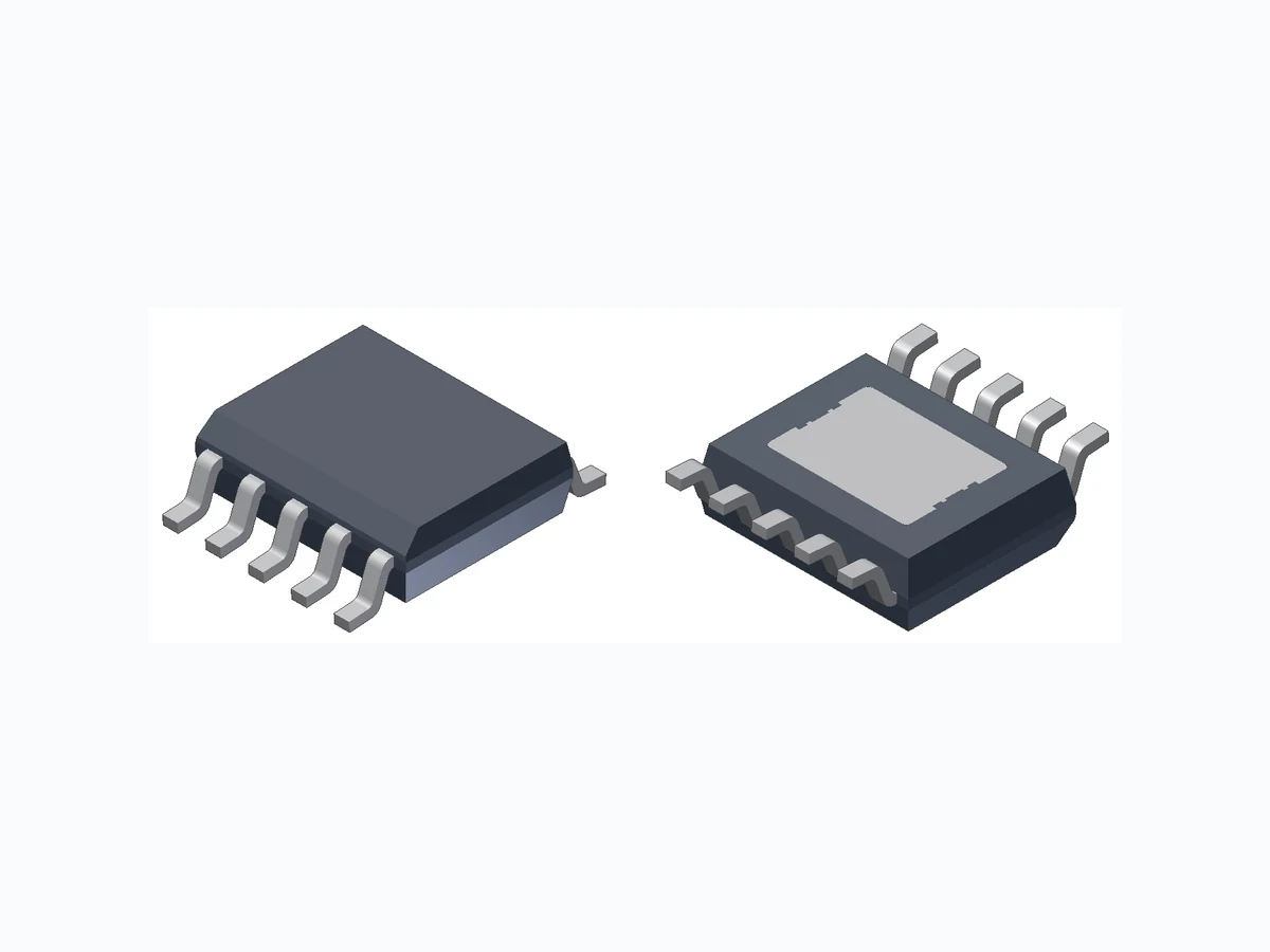
Worcester, Massachusetts 01615-0036 U.S.A. Absolute Maximum Ratings* Characteristic Symbol Notes Rating Unit Input Voltage (VIN pins) VIN –0.3 to 40 V Switching Node Voltage (SW pin) VSW Continuous; rating is a function of temperature –0.3 to VIN + 0.3 V t < 50 ns –1.0 to VIN + 3 V BOOT Pin Voltage VBOOT Continuous VSW – 0.3 to VSW + 5.5 V BOOT pin overvoltage fault condition VSW – 0.3 to VSW + 7 V VOUT Pin Voltage VOUT Continuous –0.3 to 5.5 V VOUT pin overvoltage fault condition –0.3 to 7 V PWM/PFM Pin Voltage VPWM/PFM A8585, A8585-1 –0.3 to VIN + 0.3 V EN/SLEEP Pin Voltage VEN/SLEEP A8585-2, A8585-3 –0.3 to VIN + 0.3 V All other pins –0.3 to 5.5 V Maximum Junction Temperature TJ(max) 150 ºC Storage Temperature Tstg –55 to 150 ºC *Operation at levels beyond the ratings listed in this table may cause permanent damage to the device. The Absolute Maximum ratings are stress ratings only, and functional operation of the device at these or any other conditions beyond those indicated in the Electrical Characteristics table is not implied. Exposure to Absolute Maximum-rated conditions for extended periods may affect device reliability. Selection Guide Part Number Packing* Output Voltage Option Function Option A8585KLKTR-T 3000 pieces per 13-in. reel 5 V compatible Selectable PWM / Low IQ PFMA8585KLKTR-1-T 3000 pieces per 13-in. reel 3.3 V compatible A8585KLKTR-2-T Contact factory for availability 5 V compatible Selectable Sleep (automatic PWM / Low IQ PWM selection)A8585KLKTR-3-T Contact factory for availability 3.3 V compatible *Contact Allegro™ for additional packing options Extensive protection features of the A8585 include pulse-by-pulse current limit, hiccup mode short circuit protection, open/short asynchronous diode protection, BOOT open/short voltage protection, VIN undervoltage lockout, and thermal shutdown. The A8585 is supplied in a 10-pin SOIC package (suffix LK) with exposed power pad. It is lead (Pb) free, with 100% matte-tin leadframe plating.
- Active low NPOR output with 7.5 ms delay
- Pre-bias startup capable: VOUT increases monotonically, will not cause a reset
- External compensation for maximum flexibility
- Stable with ceramic or electrolytic output capacitors
- Internally fixed soft start time of 5 ms
- Pulse-by-pulse current limit, hiccup mode short circuit, and thermal protections
- Pin open/short and component fault tolerant
- -40°C to 150°C operating junction temperature range
- Thermally enhanced SOIC-10 surface mount package Features and Benefits (continued) Description (continued) Thermal Characteristics may require derating at maximum conditions, see Power Dissipation and Thermal Calculations section Characteristic Symbol Test Conditions* Value Unit Package Thermal Resistance RθJA On 4-layer PCB based on JEDEC standard 35 ºC/W *Additional thermal information available on the Allegro website.
Wide Input Voltage, 2 A Buck Regulator Family with Low IQ ModeA8585 Allegro MicroSystems, LLC Worcester, Massachusetts 01615-0036 U.S.A. Table of Contents Specifications 1 Typical Application Diagram 1 Ordering Selection Guide 2 Absolute Maximum Ratings 2 Thermal Characteristics 2 Functional Block Diagram 4 Pin-out Diagrams and Terminal List 5 Electrical Characteristics 6 Characteristic Performance 10 Functional Description 15 Overview 15 Reference Voltage 15 PWM Switching Frequency 15 EN/SLEEP Input (for A8585-2 and A8585-3) 16 PWM/PFM Input (for A8585 and A8585-1) 16 PWM Synchronization 16 Transconductance Error Amplifier 16 Slope Compensation 16 Current Sense Amplifier 16 Power MOSFETs 17 BOOT Regulator 17 Pulse Width Modulation (PWM) Mode 17 Low-IQ Pulse Frequency Modulation (PFM) Mode 17 Soft Start (Startup) and Inrush Current Control 18 Pre-Biased Startup 19 Active Low Power-On Reset (NPOR) Output 19 Protection Features 19 Undervoltage Lockout (UVLO) 19 Pulse-by-Pulse Overcurrent Protection (OCP) 20 Overcurrent Protection (OCP) and Hiccup Mode 20 BOOT Capacitor Protection 20 Asynchronous Diode Protection 21 Overvoltage Protection (OVP) 21 Pin-to-Ground and Pin-to-Pin Short Protections 21 Thermal Shutdown (TSD) 21 Design and Component Selection 23 PWM Switching Frequency (RFSET) 23 Output Inductor (LO ) 23 Output Capacitors 24 Low-IQ PFM Output Voltage Ripple Calculation 25 Input Capacitors 26 Asynchronous Diode (D1) 27 Bootstrap Capacitor 27 Compensation Components (RZ, CZ , and CP) 27 A Generalized Tuning Procedure 30 Power Dissipation and Thermal Calculations 31 PCB Component Placement and Routing 32 Package Drawing 34
Wide Input Voltage, 2 A Buck Regulator Family with Low IQ ModeA8585 Allegro MicroSystems, LLC Worcester, Massachusetts 01615-0036 U.S.A. SQ RQ SW COMPVOUT PULL DOWN Current Comp ERROR AMP GCSA ISENSE 800 mV BG TG 400 mV 2V, 4.1V 5 . 0V BOOT+ OC 250mA BOOT REG . BOOT > 4. 1V EN BOOT REG Q BOOT FAULT BOOT OFF Ftimer hold of f B < 0.2V 3. 5 A CLAMP OCL VREG VOUT↑>3. 1V LDO REGOK 2.90 V 1.2VBG VREG D EL AY 224us↓EN/ SLEEP LDO OFF Digital PFM Controller FSET/ SYNC FB < 0.4V blankOn minOff PWM PWM PFM D EL AY 2048 ↓ FAULT LOGIC (See Fault Ta b le ) NPOR VIN VIN D EL AY 7.5ms↓ FB<740 mV FB>880 mV TSD DIODEOK UVLO Q FB> 880mV OCL BOOT FAULT DIODEOK UVLO REGOK BOOT OFF BOOT OFF F F/2 F/4 3.8V 3.4V IRAM P 1.22V 1.16V VOUT PFMready 800 mA CLAMP COMPLO PFMready FBHI Calibration VOUT Z Check COMPLO 120↑ REGOK openBIAS openBIAS 5ms voutOpen PULL DOWN F>200K Hz FB A8585-2 and A8585-3 only A8585 and A8585-1 only Functional Block Diagram
Wide Input Voltage, 2 A Buck Regulator Family with Low IQ ModeA8585 Allegro MicroSystems, LLC Worcester, Massachusetts 01615-0036 U.S.A. Pin-out Diagrams 5 6
10 BOOT
A8585 and A8585-1 variants A8585-2 and A8585-3 variants Terminal List Table Number Name Function 1, 2 VIN Power input for the control circuits and the drain of the internal high-side N-channel MOSFET. Connect this pin to a power supply of 4.0 to 35 V. A high quality, high frequency ceramic capacitor should be placed and grounded very close to this pin. PWM/PFM (A8585 and A8585-1) Setting this pin high forces PWM mode. Setting this pin low allows Low IQ PFM mode after 2048 clock cycles if two conditions are met: (1) the regulator is lightly loaded and (2) there is no clock signal being applied to the FSET/SYNCPWM input pin. EN/SLEEP (A8585-2 and A8585-3) This pin must be set high to enable the device. If this pin is set low, the device will enter a very low current shut down or sleep state (VOUT = 0 V). If the application does not require a sleep mode, then this pin can be tied directly to VIN. Do not float this pin.
4 FSET/SYNCPWM
Frequency setting and PWM synchronization pin. A resistor, RFSET , from this pin to GND sets the PWM switching frequency. See figure 11 and/or equation 1 to determine the value of RFSET. Applying a clock signal to this pin forces PWM mode (that is, it overrides a logic low on the PWM/PFM pin) and synchronizes the PWM switching frequency.
5 VOUT
Connect this pin to the output of the regulator. This pin supplies internal circuitry when its voltage level is high enough. Also, through an on-chip voltage divider, this pin connects to the negative feedback input of the error amplifier. Keep the VOUT pin quiet and kelvin connect. 6 NPOR Active low, power on reset output signal. This pin is an open drain output that transitions from low to high impedance after the output has maintained regulation for tdPOR .
7 COMP
Output of the error amplifier, and compensation node for the current mode control loop. Connect a series RC network from this pin to GND for loop compensation. See the Design and Component Selection section of this datasheet for further details. 8 GND Ground pin. 9 SW The source for the internal high-side N-channel MOSFET. The external free-wheeling diode (D1) and output inductor (LO) should be connected to this pin. Both D1 and LO should be placed close to this pin and connected with relatively wide traces. 10 BOOT High-side gate drive boost input. This pin supplies the drive for the high-side N-channel MOSFET. Connect a 47 nF ceramic capacitor from BOOT to SW. – PAD Exposed pad of the package providing enhanced thermal dissipation. This pad must be connected to the ground plane(s) of the PCB with at least 6 vias, directly in the pad.
Wide Input Voltage, 2 A Buck Regulator Family with Low IQ ModeA8585 Allegro MicroSystems, LLC Worcester, Massachusetts 01615-0036 U.S.A. ELECTRICAL CHARACTERISTICS1 Valid at 4.0 V ≤ VIN ≤ 35 V, −40°C ≤ TA = TJ ≤ 150ºC; unless otherwise specified Characteristic Symbol Test Conditions Min. Typ. Max. Unit Input Voltage Input Voltage Range2 VIN 4.0 − 35 V VIN Undervoltage Lockout Start Threshold VUVLO(ON) VIN rising 3.6 3.8 4.0 V VIN Undervoltage Lockout Stop Threshold VUVLO(OFF) VIN falling 3.2 3.4 3.6 V VIN Undervoltage Hysteresis VUVLO(HYS) − 400 − mV Input Supply Current Input Supply Current (Not in PFM) IIN IOUT = 0 mA − 2.5 3.5 mA Input Supply Current (Low IQ PFM) 3,4 ILO_IQ (0A,5.0V) A8585 VIN = 12 V, VOUT = 5.0 V, VPWM/PFM ≤ 1.2 V, IOUT = No Load, TA = 25ºC − 10 14 µA VIN = 12 V, VOUT = 5.0 V, VPWM/PFM ≤ 1.2 V, IOUT = No Load, TA = 65ºC − 15 − µA ILO_IQ (40µA,5.0V) A8585 VIN = 12 V, VOUT = 5.0 V, VPWM/PFM ≤ 1.2 V, IOUT = 40 µA, TA = 25ºC − 28 33 µA VIN = 12 V, VOUT = 5.0 V, VPWM/PFM ≤ 1.2 V, IOUT = 40 µA, TA = 65ºC − 33 − µA ILO_IQ (0A,3.3V) A8585-1 VIN = 12 V, VOUT = 3.3 V, VPWM/PFM ≤ 1.2 V, IOUT = No Load, TA = 25ºC − 7 10 µA VIN = 12 V, VOUT = 3.3 V, VPWM/PFM ≤ 1.2 V, IOUT = No Load, TA = 65ºC − 12 − µA ILO_IQ (40µA,3.3V) A8585-1 VIN = 12 V, VOUT = 3.3 V, VPWM/PFM ≤ 1.2 V, IOUT = 40 µA, TA = 25ºC − 20 24 µA VIN = 12 V, VOUT = 3.3 V, VPWM/PFM ≤ 1.2 V, IOUT = 40 µA, TA = 65ºC − 25 − µA Input Supply Current (Sleep Mode) IIN(SLEEP) A8585-2 A8585-3 VEN/SLEEP = 0 V, TJ ≤ 85°C, VIN = 16 V − 5 15 µA VEN/SLEEP = 0 V, TJ ≤ 85°C, VIN = 35 V − 7 25 µA Voltage Regulation Output Voltage Accuracy5 EVOUT (5.0V) A8585 A8585-2 0ºC < TJ < 85ºC, VOUT = 4 × VCOMP 4.950 5.0 5.050 V –40ºC < TJ < 150ºC, VOUT = 4 × VCOMP 4.925 5.0 5.075 V EVOUT (3.3V) A8585-1 A8585-3 0ºC < TJ < 85ºC, VOUT = 2 × VCOMP 3.267 3.3 3.333 V –40ºC < TJ < 150ºC, VOUT = 2 × VCOMP 3.250 3.3 3.350 V Output Dropout Voltage4 VO(PWM) VIN = 5.8 V, IOUT = 1 A, fOSC = 300 kHz 4.9 − − V VIN = 6.3 V, IOUT = 2 A, fOSC = 300 kHz 4.9 − − V Low IQ Mode Ripple3,4 VPP(LO_IQ) 8 V < VIN < 12 V − 25 65 mVPP Low IQ Peak Current Threshold IPEAK(LO_IQ) 640 800 930 mAPEAK Continued on the next page… 1Negative current is defined as coming out of the node or pin, positive current is defined as going into the node or pin. 2Thermally limited depending on input voltage, output voltage, duty cycle, regulator load currents, PCB layout, and airflow. 3Configured as shown in Typical Application diagram. 4Ensured by design and characterization, not production tested. 5At 0ºC < TJ < 85ºC, ensured by design and characterization, not production tested.
Wide Input Voltage, 2 A Buck Regulator Family with Low IQ ModeA8585 Allegro MicroSystems, LLC Worcester, Massachusetts 01615-0036 U.S.A. ELECTRICAL CHARACTERISTICS1 (continued) Valid at 4.0 V ≤ VIN ≤ 35 V, −40°C ≤ TA = TJ ≤ 150ºC; unless otherwise specified Characteristic Symbol Test Conditions Min. Typ. Max. Unit Error Amplifier Open Loop Voltage Gain AVOL VCOMP = 1.2 V − 65 − dB Transconductance with On-Chip Resistor Divider Included gm(5.0V) A8585 A8585-2 2.5 V < VOUT 88.0 120.0 152.0 μA/V 0 V < VOUT < 2.5 V 46.4 64.0 81.6 μA/V gm(3.3V) A8585-1 A8585-3 1.65 V < VOUT 133.3 181.8 230.3 μA/V 0 V < VOUT < 1.65 V 70.3 97.0 123.6 μA/V Output Current IEA VCOMP = 1.2 V − ±75 − μA Internal MOSFET Parameters2 High-Side MOSFET4 RDS(on)HS TJ = 25ºC, VBOOT – VSW = 4.5 V, IDS = 1.0 A − 110 130 mΩ High-Side MOSFET Leakage5 ILKGHS TJ < 85ºC, VEN/SLEEP ≤ 0.8 V, VSW = 0 V, VIN = 16 V − − 10 µA TJ ≤ 150ºC,VEN/SLEEP ≤ 0.8 V, VSW = 0 V, VIN = 16 V − 60 150 µA SW Node Rising/Falling Slew Rate4 SR VIN = 12 V, IOUT = 1 A − 0.72 − V/ns Low-Side MOSFET RDS(on)LS TJ = 25ºC, VIN ≥ 6 V, IDS = 0.1 A − − 10 Ω BOOT Regulator BOOT Voltage Enable Threshold VBOOT(TH) VBOOT rising 1.8 2.0 2.2 V BOOT Voltage Enable Hysteresis VBOOT(HYS) − 400 − mV Oscillator and PWM Timing PWM Switching Frequency fOSC RFSET = 86.6 kΩ 270 300 330 KHz RFSET = 61.9 kΩ 373 415 457 KHz RFSET = 45.3 kΩ 495 550 605 KHz PWM Frequency Dithering fDITHER No dithering with synchronization − ±7.5 − % Minimum Controllable On-Time tON(MIN) VIN = 12 V, IOUT = 1 A − 100 140 ns Minimum Switch Off-Time tOFF(MIN) VIN = 12 V, IOUT = 1 A − 135 160 ns FSET/SYNCPWM Synchronization Timing Synchronization Frequency Range fSW_MULT 375 − 605 KHz Synchronization Input Duty Cycle DSYNC − − 80 % Synchronization Input Pulse Width twSYNC 200 − − ns Synchronization Input Rise Time4 trSYNC − 10 15 ns Synchronization Input Fall Time4 tfSYNC − 10 15 ns Synchronization Rising Threshold4 VSYNC LO VFSET/SYNCPWM Rising − − 1.5 V Synchronization Falling Threshold4 VSYNC HI VFSET/SYNCPWM Falling 0.9 − − V Continued on the next page… 1Negative current is defined as coming out of the node or pin, positive current is defined as going into the node or pin. 2Thermally limited depending on input voltage, output voltage, duty cycle, regulator load currents, PCB layout, and airflow. 3Configured as shown in Typical Application diagram. 4Ensured by design and characterization, not production tested. 5At 0ºC < TJ < 85ºC, ensured by design and characterization, not production tested.
Wide Input Voltage, 2 A Buck Regulator Family with Low IQ ModeA8585 Allegro MicroSystems, LLC Worcester, Massachusetts 01615-0036 U.S.A. ELECTRICAL CHARACTERISTICS1 (continued) Valid at 4.0 V ≤ VIN ≤ 35 V, −40°C ≤ TA = TJ ≤ 150ºC; unless otherwise specified Characteristic Symbol Test Conditions Min. Typ. Max. Unit Current Control Loop PWM Pulse-by-Pulse Limit ILIM(TONMIN) tON = tON(MIN)PWM 3.0 3.5 4.0 A ILIM(TONMAX) tON = (1 / fSW) – tOFF(MIN)PWM , no PWM synchronization 2.0 2.6 3.0 A COMP to SW Current Gain gmPOWER − 3 − A/V Slope Compensation SE During synchronization − 0.35 − A/μs RFSET = 86.6 kΩ 0.20 0.25 0.30 A/μs RFSET = 61.9 kΩ 0.27 0.34 0.41 A/μs RFSET = 45.3 kΩ 0.36 0.45 0.54 A/μs Soft Start Soft Start Ramp Time tSS 2.5 5.0 7.5 ms Soft Start Switching Frequency fSS(5.0V) A8585 A8585-2 0 V < VOUT < 1.25 V − fOSC / 4 − kHz 1.25 V < VOUT < 2.5 V fOSC / 2 kHz
2.5 V < VOUT − fOSC − kHz
fSS(3.3V) A8585-1 A8585-3 0 V < VOUT < 0.825 V − fOSC / 4 − kHz 0.825 V < VOUT < 1.65 V fOSC / 2 kHz
1.65 V < VOUT − fOSC − kHz
Hiccup Off-Time HICOFF All hiccup faults such as VOUT shorted to GND − 20 − ms Hiccup Overcurrent Protection (OCP) Count OCPLIM t > tSS , OCP pulses − 120 − counts Hiccup BOOT Shorted Count BOOTUV − 64 − counts Hiccup BOOT Open Count BOOTOV − 7 − counts PWM/PFM Pin Input Thresholds PWM Threshold (High) VIH A8585 4.5 V < VOUT < 5.5 V, VPWM/PFM rising − − 2.6 V A8585-1 3.0 V < VOUT < 3.6 V, VPWM/PFM rising − − 2.0 V PFM Threshold (Low) VIL A8585 4.5 V < VOUT < 5.5 V, VPWM/PFM falling 1.2 − − V A8585-1 3.0 V < VOUT < 3.6 V, VPWM/PFM falling 0.8 − − V PWM/PFM Hysteresis VHYS A8585 4.5 V < VOUT < 5.5 V, VIH – VIL − 400 − mV A8585-1 3.0 V < VOUT < 3.6 V, VIH – VIL − 200 − mV PWM/PFM Pin Input Resistance RIN A8585, A8585-1 120 200 280 kΩ PWM/PFM Turn-Off Delay tdLO_IQ A8585, A8585-1 From PWM/PFM transitioning low, or NPOR transitioning high, to start Low IQ mode − 2048 − counts Continued on the next page… 1Negative current is defined as coming out of the node or pin, positive current is defined as going into the node or pin. 2Thermally limited depending on input voltage, output voltage, duty cycle, regulator load currents, PCB layout, and airflow. 3Configured as shown in Typical Application diagram. 4Ensured by design and characterization, not production tested. 5At 0ºC < TJ < 85ºC, ensured by design and characterization, not production tested.
Wide Input Voltage, 2 A Buck Regulator Family with Low IQ ModeA8585 Allegro MicroSystems, LLC Worcester, Massachusetts 01615-0036 U.S.A. ELECTRICAL CHARACTERISTICS1 (continued) Valid at 4.0 V ≤ VIN ≤ 35 V, −40°C ≤ TA = TJ ≤ 150ºC; unless otherwise specified Characteristic Symbol Test Conditions Min. Typ. Max. Unit Thermal Protection Thermal Shutdown Threshold (Rising) TSDth PWM stops immediately, COMP is pulled low, and soft start is reset 155 170 − ºC Thermal Shutdown Hysteresis TSDHYS − 20 − ºC Power On Reset (NPOR) Output NPOR Overvoltage Threshold, 5.0V VNPOROV (5.0V) VOUT rising 5.37 5.5 5.75 V NPOR Overvoltage Hysteresis, 5.0V VNPOROV (HYS)(5.0V) VOUT falling, relative to VNPOROV − -60 − mV NPOR Undervoltage Hysteresis, 5.0V VNPORUV (HYS)(5.0V) VOUT rising, relative to VNPORUV − 60 − mV NPOR Overvoltage Hysteresis, 3.3V VNPOROV (HYS)(3.3V) VOUT falling, relative to VNPOROV − -40 − mV NPOR Undervoltage Hysteresis, 3.3V VNPORUV (HYS)(3.3V) VOUT rising, relative to VNPORUV − 40 − mV NPOR Overvoltage Delay tdPOV_POR VOUT falling beyond VNPOROV − 120 − counts NPOR Delay to Rising Edge tdPOR VOUT rising only 5 7.5 10 ms NPOR Low Output Voltage VPOROL INPOR = 4 mA − 200 400 mV NPOR Leakage ILKGPOR VNPOR = 5.5 V − − 1.2 µA EN/SLEEP Pin Input Thresholds EN/SLEEP Threshold (High) VSLEEPVIH A8585-2 A8585-3 VEN/SLEEP rising − 1.3 2.1 V EN/SLEEP Threshold (Low) VSLEEPVIL A8585-2 A8585-3 VEN/SLEEP falling 0.5 1.2 − V EN/SLEEP Delay tdSLEEP A8585-2 A8585-3 VEN/SLEEP transitioning low 115 224 300 µs EN/SLEEP Input Bias Current IBIASSLEEP A8585-2 A8585-3 VEN/SLEEP = 5 V − 500 − nA 1Negative current is defined as coming out of the node or pin, positive current is defined as going into the node or pin. 2Thermally limited depending on input voltage, output voltage, duty cycle, regulator load currents, PCB layout, and airflow. 3Configured as shown in Typical Application diagram. 4Ensured by design and characterization, not production tested. 5At 0ºC < TJ < 85ºC, ensured by design and characterization, not production tested.
Wide Input Voltage, 2 A Buck Regulator Family with Low IQ ModeA8585 Allegro MicroSystems, LLC Worcester, Massachusetts 01615-0036 U.S.A. Characteristic Performance Output Voltage versus Temperature VIN UVLO Start and Stop Thresholds versus Temperature versus Temperature Pulse-by-Pulse Current Limit at tON(MIN) versus Temperature Error Amplifier Transconductance Error Amplifier Transconductance versus Temperature Output V oltage, V (V) OUT Temperature (°C) Oscillator Frequency , f (kHz) OSC Temperature (°C) Input Voltage, V (V) IN Temperature (°C) I (A)LIM(TONMIN) Temperature (°C) Temperature (°C) Transconductance, g (µA/V) m Transconductance, g (µA/V) m Temperature (°C) V = 5.0 VOUT V = 3.3 VOUT V = 5.0 VOUT V = 3.3 VOUT f = 300 kHzOSC f = 415 kHzOSC f = 550 kHzOSC VIN Undervoltage Lockout Stop Threshold, VUVLO(OFF) VIN Undervoltage Lockout Start Threshold, VUVLO(ON) 5.5 5.0 4.5 4.0 3.5 3.0 2.5 2.0 3.9 3.8 3.7 3.6 3.5 3.4 3.3 140 120 100 200 180 160 140 120 100 600 550 500 450 400 350 300 250 200 3.55 3.50 3.45 3.40 3.35 3.30 3.25 -50 50 75 100 125 150 175-25 250 -50 50 75 100 125 150 175-25 250 -50 50 75 100 125 150 175-25 250 -50 50 75 100 125 150 175-25 250 -50 50 75 100 125 150 175-25 250 -50 50 75 100 125 150 175-25 250 Switching Frequency versus Temperature V > 2.5 VIN V < 2.5 VIN V > 1.65 VIN V < 1.65 VIN
Wide Input Voltage, 2 A Buck Regulator Family with Low IQ ModeA8585 Allegro MicroSystems, LLC Worcester, Massachusetts 01615-0036 U.S.A. V = 5.0 VOUT V = 3.3 VOUT V = 5.0 VOUT V = 3.3 VOUT PWM/PFM High and Low Voltage Thresholds NPOR Overvoltage and Undervoltage Thresholds NPOR Low Output Voltage versus Temperature NPOR Overvoltage and Undervoltage Thresholds versus Temperature versus Temperature PWM/PFM High and Low Voltage Thresholds versus Temperature versus Temperature NPOR Time Delay versus Temperature PWM/PFM Pin Input V oltage (V) NPOR Pin V oltage (V) NPOR Pin V oltage (V) PWM/PFM Pin Input V oltage (V) Temperature (°C) Temperature (°C) Temperature (°C) Temperature (°C) NPOR Pin Output V oltage (mV) Temperature (°C) NPOR Delay to Rising Edge t (ms) dPOR Temperature (°C) I = 2 mAOUT 1.90 1.85 1.80 1.75 1.70 1.65 1.60 5.8 5.6 5.4 5.2 5.0 4.8 4.6 4.4 4.2 4.0 300 250 200 150 100 8.20 8.15 8.10 8.05 8.00 7.95 7.90 7.85 7.80 7.75 1.30 1.28 1.26 1.24 1.22 1.20 1.18 1.16 1.14 3.8 3.6 3.4 3.2 3.0 2.8 2.6 2.4 2.2 2.0 -50 50 75 100 125 150 175-25 250 -50 50 75 100 125 150 175-25 250 -50 50 75 100 125 150 175-25 250 -50 50 75 100 125 150 175-25 250 -50 50 75 100 125 150 175-25 250 -50 50 75 100 125 150 175-25 250 VIL VIH VNPOROV(5.0V) VNPORUV(5.0V) VNPOROV(3.3V) VNPORUV(3.3V) VIL VIH
Wide Input Voltage, 2 A Buck Regulator Family with Low IQ ModeA8585 Allegro MicroSystems, LLC Worcester, Massachusetts 01615-0036 U.S.A. Dropout Operation – Typical and Worst Case Operation Output Voltage, VOUT (V) Input Voltage, VIN (V) Typical Output Voltage versus Input Voltage at High Ambient at 100%, 66%, and 33% Load Worst Case Output Voltage versus Input Voltage at High Ambient at 100%, 66%, and 33% Load Output Voltage, VOUT (V) Input Voltage, VIN (V) IOUT = 0.67 A IOUT = 2.00 A IOUT = 1.33 A IOUT = 0.67 A IOUT = 2.00 A IOUT = 1.33 A
Wide Input Voltage, 2 A Buck Regulator Family with Low IQ ModeA8585 Allegro MicroSystems, LLC Worcester, Massachusetts 01615-0036 U.S.A. Figure 1: PWM/PFM Mode Timing Diagram 204820482048 STATE PWM/PFM (MODE) VIN VOUT SW Fosc SS PWM LOW IQ PFM Fosc OFF PWM FOSC/4 FOSC/2 IOUT 100mA PWM/PFM is low and IL_PK < IPEAK,LO_IQ PWM LOW IQ PFM PWM Pulse Skipping at Fosc BC NPOR tdPOR COMP No Load Fosc LOW IQ PFM UVLO OFF COMP pulled up to set IPEAK,LO_IQ MLKIFEDA IL_PK > IPEAK,LO_IQ G H 100mA VOUT< NPORUV VOUT< VREGOK VOUT< VOUTHI UVLO or other faults J A The output voltage reaches regulation voltage after soft start startup. The A8585 family always starts in PWM mode, independent of the PWM/PFM signal. B NPOR transitions high after NPOR delay (7.5 ms (typ)). C PWM/PFM signal is logic low, so the device enters Low IQ PFM mode after NPOR transitions high and 2048 clock cycles expire. D The output current increases and, even though PWM/PFM is low, the device transitions to PWM mode to maintain optimal regulation. E PWM/PFM transitions low after transitioning high, 2048 clock cycles occur, but the device stays in PWM mode because the output current is too high. F The output current decreases and PWM/PFM has been low for a relatively long time, so the device enters Low IQ PFM mode. G PWM/PFM transitions high so the device is forced into PWM mode immediately, independent of the load current. If the output is at no load condition, then the device starts pulse skipping with COMP hovering around the 400mV pedestal. H The output current increases from no load condition, and the device stops pulse skipping and starts switching again at fOSC . I The output current is low, PWM/PFM transitions low, and 2048 clock cycles later, the device enters Low IQ PFM mode due to low current. J VIN has been removed but the circuit is still powered from the VOUT pin. In addition, all faults are ignored while VOUT > VOUTHI. K When VOUT drops below VOUTHI (1% above the regulation point) all faults are checked. UVLO is active, so the COMP pin is pulled low and switching is disabled. L When VOUT drops below the VNPORUV threshold, NPOR transitions low. M When VOUT drops below VREGOV , the device is completely turned off.
Wide Input Voltage, 2 A Buck Regulator Family with Low IQ ModeA8585 Allegro MicroSystems, LLC Worcester, Massachusetts 01615-0036 U.S.A. Figure 2: Operation with PWM/PFM = 0 OVP MODE TSD OC HIC_EN HICCUP OC FAULT BOOT FAULT VIN VOUT COMP DIODE/SW FAULT 5ms SS PWM O C 20ms HICCUP x120 x7 OV x120 UV OFF NPOR 7.5ms BOOT, DOIDE, or SW FAULTS REGOK REGOK=0 5ms SS Vout shorted to GND 5ms SS O C 20ms HICCUP 5ms SS 7.5ms PWM 20ms HICCUP 5ms SS x7 OV x120 UV 20ms HICCUP x1 x1 5ms SS 7.5ms PWM 5ms SS 7.5ms PWMSS TSD SS TSD REGOK=0 TSD 5ms SS 7.5ms PWM FSET Open or Short REGOK=0 x120 VOUT Open VOUT Pin Open BIAS Connected PFM Ready 2048 Tcal 2048 Tcal 2048 Tcal 2048 Tcal Tcal PFM Light OVP Heavy OVP PFM Wakeup and Check Faults 120 7.5ms 2048 Tcal PWM SW f SW f SW/4 f SW/4 then f SW/2 f SW/4 f SW f SW/4 then f SW/2 f SW f SW/4 then f SW/2 f SWf SW f SW f SW f SW/4 then f SW/2 LS SW & HSPD LS SW & HSPD LS SW & HSPD f SW 5ms SS 7.5ms PWM Tcal f SW f SW/4 then f SW/2 0 to 1.5V at 32x period REGOK=0 2048 2048
Wide Input Voltage, 2 A Buck Regulator Family with Low IQ ModeA8585 Allegro MicroSystems, LLC Worcester, Massachusetts 01615-0036 U.S.A. Functional Description Overview The A8585 family are current mode, buck regulators that incor- porate all the control and protection circuitry necessary to provide the power supply requirements of car audio and infotainment systems. The A8585 family consists of four parts: Part Number PWM Mode Selection* 10 µA Sleep Mode Output Voltage (V) A8585 yes no 5.0 A8585-1 yes no 3.3 A8585-2 (automatic) yes 5.0 A8585-3 (automatic) yes 3.3 *A synchronization signal on the FSET pin, or a heavy output load current will force all variants into PWM mode. The A8585 family has three modes of operation:
- Pulse width modulation (PWM) mode, delivering up to 2.0 A. (All variants)
- Low-IQ pulse frequency modulation (PFM) mode, drawing only approximately 10 µA from VIN while maintaining VOUT (at no load). Under most conditions, Low-IQ PFM mode is typically capable of supporting up to approximately 100 mA, depending on applications. (All variants)
- For the A8585-2 and A8585-3 variants, a third mode of opera- tion is entered when the EN/SLEEP pin is set to 0. The device enters an ultra-low current, shutdown mode. VOUT = 0 V and the total current drawn from VIN is less than 10 µA (typ). In PFM mode, the device operates with lower switching fre- quency to achieve higher efficiency at light load. When the load is heavy, the device automatically transitions into PWM mode to support a relatively higher current. For the A8585 and A8585-1 variants, setting the PWM/PFM pin high disables PFM opera- tion mode even at light load and forces the device to operate in a PWM constant frequency mode. The A8585 family is designed to support up to 2.0 A output. However, the exact amount of current it will supply, before pos- sible thermal shutdown, depends heavily on duty cycle, ambient temperature, airflow, PCB layout, and PCB construction. Figure 3 shows calculated current ratings versus ambient temperature for VIN = 12 V/VOUT = 3.3 V and for VIN = 12 V/VOUT = 5.0 V at 300 kHz and 550 kHz. This analysis assumed a 4-layer PCB according to the JEDEC standard (34°C/W), no nearby heat sources, and no airflow. Reference Voltage The A8585 family incorporates an internal reference that allows output voltages as low as 0.8 V . The accuracy of the internal ref- erence is ±1.0% for TJ from 0°C to 85°C, and ±1.5% from −40°C to 150°C. The output voltage from the device regulator is directly connected to the VOUT pin and is divided down internally to 800 mV by an internal resistor divider inside the regulator, as shown in the Functional Block diagram. The A8585 and A8585-2 variants have a fixed 5.0 V output voltage; the A8585-1 and A8585-3 variants have a fixed 3.3 V output voltage. PWM Switching Frequency The PWM switching frequency of the A8585 family is adjustable from 300 to 550 kHz and has an accuracy of ±10% over the oper- ating temperature range. The switching frequency is dithered to help reduce EMI between -7.5% and 7.5% according to a random sequence. During startup, the PWM switching frequency changes from 25%, to 50%, and finally 100% of fSW as VOUT rises from 0 V to the regulation voltage. The startup switching frequency is described in detail in the Soft Start section of this datasheet. If the regulator output is shorted to ground, VFB ≈ 0 V and the Figure 3: Typical Current Derating 0.9 1.0 1.1 1.2 1.3 1.4 1.5 1.6 1.7 1.8 1.9 2.0 2.1 75 85 95 105 115 125 Current Rating (A) Ambient Temperature (°C) 12Vin/5Vout/300kHz 12Vin/3.3Vout/300kHz 12Vin/5Vout/550kHz 12Vin/3.3Vout/550kHz
Wide Input Voltage, 2 A Buck Regulator Family with Low IQ ModeA8585 Allegro MicroSystems, LLC Worcester, Massachusetts 01615-0036 U.S.A. PWM frequency is 25% of fSW . In this case, the low switching frequency allows extra off-time between SW pulses. The extra off-time allows the inductor current to remain under control (remains well above 0) before the next SW pulse occurs. This prevents the inductor current from ratcheting up, or rising, to a value that could damage the device or the output inductor. The FSET pin includes protection features that disable the regu- lator when the FSET pin is shorted to GND, shorted High (to NPOR), or when RFSET is mis-selected. EN/SLEEP Input (for A8585-2 and A8585-3) The A8585-2 and A8585-3 variants have the EN/SLEEP logic level input pin. To enable the device, the EN/SLEEP pin must be a logic high (>2.1 V). The EN/SLEEP pin is rated to 40 V so this EN/SLEEP pin may be connected directly to VIN if there is no suitable logic signal available to wake up the regulator. When EN/SLEEP transitions low, the device waits approximately 224 µs before shutting down. This delay provides plenty of filter- ing to prevent the device from prematurely entering Sleep mode because of any small glitches that might couple onto the PCB trace or EN/SLEEP pin. PWM/PFM Input (for A8585 and A8585-1) The PWM/PFM pin provides two major functions. This pin is a control input that sets the operating mode. If PWM/PFM is logic high the device operates only in PWM mode. If PWM/ PFM is logic low the device operates in Low-IQ PFM mode if two conditions are met: (1) the regulator is lightly loaded and (2) there is no clock signal applied to the FSET/SYNCPWM input pin. If PWM/PFM transitions from logic high to logic low, the device checks that VSS > 2.3 V and NPOR = 1. If these two conditions are satisfied then the device will wait 2048 clock cycles and then enter into Low IQ PFM mode. This delay provides sufficient filtering to prevent the regulator from prematurely entering PFM mode because of any small glitches that might couple onto the PCB trace or PWM/PFM pin. PWM Synchronization If an external clock is applied to the FSET/SYNCPWM pin, the device is forced into PWM mode and synchronizes its PWM frequency to the external clock. Synchronization is independent of Rfset it only needs to satisfy the >200 KHz requirement. When synchronizing, the external clock pulses must satisfy the pulse width, duty-cycle, and rise/fall time requirements shown in the Electrical Characteristics table in this datasheet. During synchro- nization, frequency dithering is disabled. The 8585 synchronizes to the SYNC input when the FSET/ SYNCPWM pin is driven above the 1.2 V threshold. Synchroni- zation must occur within 16 μs or else a fault may be declared causing SW to halt operation. The 8585 will transition back to using the RFSET resistor after a rising has not crossed the 1.2V threshold for ~8 μs, resulting in the high side switch remaining off for ~8 μs and causing some VOUT droop. Transconductance Error Amplifier The transconductance error amplifier's primary function is to control the regulator output voltage. The error amplifier is shown in the Functional Block diagram. It is shown as a three-terminal input device with two positive inputs and one negative input. An on-chip resistor divider is included. The negative input is simply connected to the internal resistor divider and is used to sense the feedback voltage for regulation. The two positive inputs are used for soft start and steady-state regulation. The error amplifier performs an analog OR selection between the two positive inputs. The error amplifier regulates to either the internal soft start volt- age or the device internal reference, whichever is lower. To stabilize the regulator, a series RC compensation network (RZ and CZ) must be connected from the error amplifier output (the COMP pin) to GND, as shown in the Typical Application diagram. In most instances an additional, relatively low value capacitor (CP) should be connected in parallel with the RZ-CZ components to reduce the loop gain at very high frequencies. However, if the CP capacitor is too large, the phase margin of the converter can be reduced. Calculating RZ, CZ, and CP is covered in detail in the Component Selection section of this datasheet. If a fault occurs or the regulator is disabled, the COMP pin is pulled to GND via approximately 1 kΩ and SW switching is inhibited. Slope Compensation The A8585 family incorporates internal slope compensation (SE ) to allow PWM duty cycles above 50% for a wide range of input/ output voltages and inductor values. The slope compensation sig- nal is added to the sum of the current sense amplifier output and the PWM ramp offset. As shown in the Electrical Characteristics table, the amount of slope compensation scales with the nominal switching frequency (fSW) set by RFSET . The amount of slope
Wide Input Voltage, 2 A Buck Regulator Family with Low IQ ModeA8585 Allegro MicroSystems, LLC Worcester, Massachusetts 01615-0036 U.S.A. compensation scales with the SYNC input frequency centered around 0.35 A/μs at 425 kHz in a similar way with RFSET. The value of the output inductor should be chosen such that SE is between 0.5 × and 1 × the falling slope of the inductor cur- rent (SF). Current Sense Amplifier The A8585 family incorporates a high-bandwidth current sense amplifier to monitor the current in the high-side MOSFET. This current signal is used by both the PWM and PFM control cir- cuitry to regulate the MOSFET peak current. The current signal is also used by the protection circuitry to prevent damage to the device. Power MOSFETs The A8585 family includes a 40 V, 110 mΩ high-side N-channel MOSFET capable of delivering at least 2.0 A. The device also includes a 10 Ω, low-side MOSFET to help insure the boot capacitor is always charged. The typical RDS(on) increase versus temperature is shown in Figure 4. BOOT Regulator The A8585 family contains a regulator to charge the boot capaci- tor. The voltage across the BOOT capacitor typically is 5.0 V . If the boot capacitor is missing the device detects a boot over- voltage. Similarly, if the BOOT capacitor is shorted the device detects a boot undervoltage. Also, the boot regulator has a current limit to protect itself during a short circuit condition. The details of how each type of boot fault is handled by the A8585 are shown in Table 1. Pulse Width Modulation (PWM) Mode The A8585 family utilizes fixed-frequency, peak current mode control to provide excellent load and line regulation, fast transient response, and ease of compensation. A high-speed comparator and control logic, capable of typical pulse widths down to Ton(min), are included in the device. The inverting input of the PWM comparator is connected to the out- put of the error amplifier. The non-inverting input is connected to the sum of the current sense signal, the slope compensation, and a DC offset voltage (VPWMOFFS , nominally 400 mV). At the beginning of each PWM cycle, the CLK signal sets the PWM flip-flop and the high-side MOSFET is turned on. When the summation of the DC offset, slope compensation, and current sense signal, rises above the error amplifier voltage the PWM flip -flop is reset and the high-side MOSFET is turned off. The PWM flip-flop is reset dominant so the error amplifier may override the CLK signal in certain situations. For example, at very light loads or extremely high input voltages the error ampli- fier (temporarily) reduces its output voltage below the 400 mV DC offset and the PWM flip-flop ignores one or more of the incoming CLK pulses. The high-side MOSFET does not turn on and the regulator skips pulses to maintain output voltage regulation. In PWM mode, and when SW is switching in PFM mode, all of the device fault detection circuits are active. See Figure 1 showing how faults are handled during PWM mode. Also, the Protection Features section of this datasheet provides a detailed description of each fault and Table 1 presents a summary. Low-IQ Pulse Frequency Modulation (PFM) Mode The PWM/PFM variants (A8585 and A8585-1) enter Low-IQ PFM mode 2048 counts after the PWM/PFM pin goes low, provided that no faults are present, the load is light, NPOR = 1 and no external clock is applied to the FSET/SYNCPWM pin. Similarly, the EN/SLEEP variants (A8585-2 and A8585-3) enter Low-IQ PFM mode under the same conditions (except there is no PWM/PFM pin), and the EN/SLEEP pin is high. At light loads the PFM comparator, which is connected to the VOUT pin through the internal feedback resistor divider (which is the internal FB point), modulates the frequency of the SW node to regulate the output voltage with very high efficiency. Temperature (°C) -40 -20 0 20 40 60 80 100 120 140 160 1.8 1.6 1.4 1.2 1.0 0.8 0.6 0.4 0.2 Normalized R DS(on) Figure 4: Typical MOSFET RDS(on) versus Temperature
Worcester, Massachusetts 01615-0036 U.S.A. age, output voltage, slope compensation, and inductor value. (PWM operation) and then transitions back to 0.05A PFM mode. function. The soft start time of the A8585 family is fixed at 5 ms. In Figure 7 the startup sequence shows the soft start operation. Figure 7. Soft Start Operation: VOUT Ramps from Startup
Worcester, Massachusetts 01615-0036 U.S.A. when VOUT is above 50% (at C) the switching frequency is fSW. is above 50% (at C) the error amplifier gain is gm . (resistor divider) FB voltage. 200 mV , the device clears the internal fault latch. the Protections section of this datasheet. tor must be used, as shown in the Typical Application diagram. ( TSDth ). For other faults, NPOR depends on the output voltage. Figure 8. Soft Start Prebiased Startup: VOUT Prebiased at 2 V,
Wide Input Voltage, 2 A Buck Regulator Family with Low IQ ModeA8585 Allegro MicroSystems, LLC Worcester, Massachusetts 01615-0036 U.S.A. for reliable operation in this situation, the user should select an NPOR resistor (if connected to VOUT) with a low enough value to overwhelm any high-side switch leakage. Protection Features The A8585 was designed to satisfy the most demanding automo- tive and non-automotive applications. In this section, a descrip- tion of each protection feature is provided, and table 1 sum- marizes the protection operation. All faults are available in both PWM and PFM mode. In PFM mode all faults are monitored just before and while switching is active, but are ignored while VOUT remains above the PFM comparator threshold and below the NPOR OV threshold. Undervoltage Lockout (UVLO) An undervoltage lockout (UVLO) comparator monitors the volt- age at the VIN pin and keeps the regulator disabled if the voltage is below the stop threshold (VUVLO(OFF) ). The UVLO comparator incorporates some hysteresis (VUVLO(HYS) ) to help reduce on-off cycling of the regulator due to resistive or inductive drops in the VIN path during heavy loading or during startup. Pulse-by-Pulse Overcurrent Protection (OCP) The A8585 family monitors the current of the high-side MOS- FET and if the current exceeds the pulse-by-pulse overcurrent threshold (ILIM) then the high-side MOSFET is turned off. Normal PWM operation resumes on the next clock pulse from the oscillator. The device includes leading edge blanking (as defined by Ton(min) spec) to prevent false triggering of the pulse-by-pulse current limit when the high-side MOSFET is turned on initially. Because the slope compensation ramp is added to the inductor current, the A8585 family delivers more current at lower duty cycles and less current at higher duty cycles. Figure 9 illustrates the relationship between the current limit and duty cycle. As shown, the current limit at min and max duty cycle remains fixed, but the relationship vs. duty cycle is skewed with frequency due to the fixed minoff time. Given the relationship it is best to use the ILIM(tonmin) and ILIM(toffmin) to calculate the current limit at a given duty cycle. During synchronization, the slope compensation scales in a simi- lar fashion as RFSET, with slight less accuracy. The exact current the buck regulator can support is heavily dependent on duty cycle (VIN , VOUT , diode forward voltage Vf ), ambient temperature, thermal resistance of the PCB, airflow, component selection, and nearby heat sources. Overcurrent Protection (OCP) and Hiccup Mode An OCP counter and hiccup mode circuit protect the buck regula- tor when the output of the regulator is shorted to ground or when the load is too high. When the soft start ramp is active (t<tss), the OCP hiccup counter is disabled. Two conditions must be met for the OCP counter to be enabled and begin counting:
- t > tss, and
- VCOMP clamped at its maximum voltage (OCL = 1) As long as these two conditions are met the OCP counter remains enabled and counts pulses from the overcurrent comparator. If the COMP voltage decreases (OCL = 0) the OCP counter is cleared. If the OCP counter reaches OCPLIM counts (120), a hiccup latch is set and the COMP pin is quickly pulled down by a relatively low resistance (1 kΩ), and switching is halted for 20 ms to provide time for the IC to cool down. After the hiccup off-time expires (20 ms), the soft start ramp starts, marking the beginning of a new, normal soft start cycle as described earlier. When the soft start voltage crosses the effective output voltage, the error amplifier forces the voltage at the COMP pin to quickly slew upward and PWM switching resumes. If the short circuit at the regulator output remains, another hiccup cycle occurs. Hiccups repeat until the short circuit is removed or the converter is disabled. If the short circuit has been removed, the device soft starts normally and the output voltage automatically recovers to the target level, as shown in Figure 10. 2.0 2.2 2.4 2.6 2.8 3.0 3.2 3.4 3.6 3.8 4.0 4.2 0 5 10 15 20 25 30 35 40 45 50 55 60 65 70 75 80 85 90 95 100 ILIM (A) Duty Cycle, D (%) Min. 550 kHz Typ. 550 kHz Max. 550 kHz Min. 300 kHz Typ. 300 kHz Max. 300 kHz Figure 9: Pulse-by-Pulse Current Limit vs Duty Cycle at 300 kHz (dashed lines) and 550 kHz (solid lines)
Worcester, Massachusetts 01615-0036 U.S.A. tor enters hiccup mode after 120 to 64 PWM cycles. recovers when the fault is corrected. hiccup mode after detecting 1 missing diode fault. each pin without suffering damage. the voltage at the COMP pin are pulled low until VSS < VSSRST . if the junction temperature decreases by approximately 20°C. Figure 10. Hiccup Mode and Recovery (to 5.0 V at 0.5 A, for A8585/A8585-2, shown)
Wide Input Voltage, 2 A Buck Regulator Family with Low IQ ModeA8585 Allegro MicroSystems, LLC Worcester, Massachusetts 01615-0036 U.S.A. Table 1: Summary of A8585 Family Fault Modes and Operation Fault Mode Internal Soft Start During Fault Counting, Before Hiccup Mode Boot Charging NPOR Latched Fault Reset ConditionVCOMP High-Side Switch Low-Side Switch Output shorted to ground Hiccup, after
120 OCL
ILIM , then pulled low for Hiccup fOSC / 4 due to VOUT < 25%, responds to VCOMP Can be activated if BOOT voltage is too low Not affected Depends on VOUT No Automatic, remove the short Output overcurrent, VOUT > 50% Hiccup, after ILIM , then pulled low for Hiccup fOSC, responds to VCOMP Can be activated if BOOT voltage is too low Not affected Depends on VOUT No Automatic, decrease load current VOUT pin open Pulled low after 32 cycles Pulled low after 32 cycles Forced off by COMP low Can be activated if BOOT voltage is to low Not affected Stays low No Automatic, VOUT pin reconnected Boot capacitor missing Hiccup, after 7 Boot OV faults Not affected but pulled low for Hiccup Forced off when Boot OV fault occurs Forced off when Boot OV fault occurs Off after Boot fault occurs Depends on VOUT No Automatic, replace capacitor Boot capacitor shorted Hiccup, after
64 Boot UV
Automatic, unshort capacitor Asynchronous diode missing Hiccup after 1 fault Not affected but pulled low for Hiccup Forced off after 1 fault Can be activated if BOOT voltage is too low Not affected Depends on VOUT No Automatic, install diode Asynchronous diode (or SW) hard short to ground Hiccup after 1 fault Clamped for ILIM , then pulled low for Hiccup Forced off after 1 fault Can be activated if BOOT voltage is too low Not affected Depends on VOUT No Automatic, remove short Asynchronous diode (or SW) soft short to ground Hiccup, after ILIM , then pulled low for Hiccup Active, responds to VCOMP Can be activated if BOOT voltage is too low Not affected Depends on VOUT No Automatic, remove short Output overvoltage, (VOUT > 3.6 V/5.5 V) Not affected Transitions low via loop response Forced off Active during tOFF(MIN) Off when VOUT is too high Pulled low when VOUT is too high for 120 counts No Automatic, VOUT returns to normal range Output under voltage Not affected Transitions high via loop response Active, responds to VCOMP Can be activated if BOOT voltage is too low Not affected Pulled low when VOUT is too low No Automatic, VOUT returns to normal range FSET shorted to GND or above 1.0 V Pulled Low Pulled Low Forced Off Forced Off Forced Off Depends on VOUT No Auto Thermal shutdown (TSD) Pulled low until VSS<VSSRST and TSD = 0 Pulled low until VSS<VSSRST and TSD = 0 Forced Off Disabled Off Pulled Low No Auto, part cools down
Wide Input Voltage, 2 A Buck Regulator Family with Low IQ ModeA8585 Allegro MicroSystems, LLC Worcester, Massachusetts 01615-0036 U.S.A. PWM Switching Frequency (RFSET) The PWM switching frequency is set by connecting a resistor from the FSET/SYNCPWM pin to ground. Figure 11 is a graph showing the relationship between the typical switching frequency (y-axis) and the FSET resistor (x-axis). For a required switching frequency ( fSW ), the FSET resistor value can be calculated as follows: = – 4.7827770 fSW RFSET (1) where fSW is in kHz and RFSET is in kΩ. When the PWM switching frequency is chosen, the user should be aware of the minimum controllable on-time ( tON( MIN) ) and minimum off time of the A8585 family. If the system required on- time is less than tON( MIN) then switch node jitter occurs and the output voltage has increased ripple or oscillations. The PWM switching frequency should be calculated as follows: = tON(MIN) ×VIN(MAX) VOUTfSW (2) where VOUT is the output voltage, tON(MIN) is the minimum controllable on-time of the A8585 family (100 ns (typ), 140 ns (max) ), and VIN(MAX) is the maximum required operational input voltage (not the peak surge voltage). If the device synchronization function is employed, then the base switching frequency should be chosen such that jitter does not result at the maximum synchronized switching frequency accord- ing to equation 2. Output Inductor (LO ) For a peak current mode regulator it is common knowledge that, without adequate slope compensation, the system becomes unstable when the duty cycle is near or above 50%. However, the slope compensation in the A8585 family is a fixed value (SE ). Therefore, it is important to calculate an inductor value such that the falling slope of the inductor current ( SF ) works well with the device slope compensation. Equations 3a and 3b can be used to calculate a range of values for the output inductor based on the well known approach of providing slope compensation that matches 50% to 100% of the down slope of the inductor current. ≤≤ LO2 × SE VOUT +Vf VOUT +Vf SE (3a) where LO is in µH, Vf is the forward voltage of the asynchronous diode, and the slope compensation (SE ) is a function of switching frequency, as follows: SE = 0.13 × f 2 SW + 0.69 × f SW+ 0.031 (3b) where SE is in A/µs and fSW is in MHz. More recently, Dr. Raymond Ridley presented a formula to calculate the amount of slope compensation required to critically damp the double poles at half the PWM switching frequency (this approach includes the duty cycle (D), which should be calculated at the minimum input voltage to insure optimal stability): ≥LO 1 – VIN(MIN) + VfVOUT + Vf VOUT + VfSE 0.18 × (4) To avoid dropout (saturation of the buck regulator), VIN(MIN) must be approximately 1 to 1.5 V above VOUT when calculating the inductor value with equation 4. If equations 3a or 4 yield an inductor value that is not a standard value then the next closest available value should be used. The final inductor value should allow for 10% to 20% of initial toler- Design and Component Selection Figure 11: PWM Switching Frequency versus RFSET 650 600 550 500 450 400 350 300 250 200 150 40 45 50 55 60 65 70 75 80 85 90 95 100 FSET Resistor, RFSET (kΩ) Swtiching Frequency, fSW (kHz)
Wide Input Voltage, 2 A Buck Regulator Family with Low IQ ModeA8585 Allegro MicroSystems, LLC Worcester, Massachusetts 01615-0036 U.S.A. ance and 20% to 30% of inductor saturation. The saturation current of the inductor should be higher than the peak current capability of the device. Ideally, for output short circuit conditions, the inductor should not saturate given the high- est pulse-by-pulse current limit at minimum duty cycle (ILIM(0)), 4.0 A (max). This may be too costly. At the very least, the induc- tor should not saturate given the peak operating current according to the following equation: =IPEAK 4.1 – SE × (VOUT + Vf ) 1.15 × fSW × (VIN(MAX) + Vf ) (5) where VIN(MAX) is the maximum continuous input voltage, such as 18 V (not a surge voltage, like 40 V). Starting with equation 5 and subtracting half of the inductor ripple current provides us with an interesting equation to predict the typical DC load capability of the regulator at a given duty cycle (D): ≤IOUT(DC) 4.1 – –SE × D VOUT × (1 – D ) 2 × fSW × LOfSW (6) After an inductor is chosen it should be tested during output short circuit conditions. The inductor current should be monitored using a current probe. A good design should ensure the inductor or the regulator are not damaged when the output is shorted to ground at maximum input voltage and the highest expected ambi- ent temperature. Output Capacitors The output capacitors filter the output voltage to provide an acceptable level of ripple voltage, and they also store energy to help maintain voltage regulation during a load transient. The voltage rating of the output capacitors must support the output voltage with sufficient design margin. The output voltage ripple (ΔVOUT ) is a function of the output capacitor parameters: CO , ESRCO , and ESLCO: =∆VOUT ∆IL × ESRCO ∆IL × ESLCO VIN – VOUT LO 8 fSWCO (7) The type of output capacitors determines which terms of equa- tion 7 are dominant. For ceramic output capacitors the ESRCO and ESLCO are virtually zero, so the output voltage ripple will be dominated by the third term of equation 7: ≤∆VOUT ∆IL 8 fSWCO (8) To reduce the voltage ripple of a design using ceramic output capacitors simply: increase the total capacitance, reduce the inductor current ripple (that is, increase the inductor value), or increase the switching frequency. For electrolytic output capacitors the value of capacitance will be relatively high, so the third term in equation 7 will be very small and the output voltage ripple will be determined primarily by the first two terms of equation 7: =∆VOUT ∆IL × ESRCO × ESLCO VIN LO (9) To reduce the voltage ripple of a design using electrolytic output capacitors simply: decrease the equivalent ESRCO and ESLCO by using a high(er) quality capacitor, or add more capacitors in parallel, or reduce the inductor current ripple (that is, increase the inductor value). The ESR of some electrolytic capacitors can be quite high so Allegro recommends choosing a quality capacitor for which the ESR or the total impedance is clearly documented in the capaci- tor datasheet. Also, the ESR of electrolytic capacitors usually increases significantly at cold ambients, as much as 10 X, which increases the output voltage ripple and, in most cases, reduces the stability of the system.
Wide Input Voltage, 2 A Buck Regulator Family with Low IQ ModeA8585 Allegro MicroSystems, LLC Worcester, Massachusetts 01615-0036 U.S.A. The transient response of the regulator depends on the quantity and type of output capacitors. In general, minimizing the ESR of the output capacitance will result in a better transient response. The ESR can be minimized by simply adding more capacitors in parallel or by using higher quality capacitors. At the instant of a fast load transient (di/dt), the output voltage changes by the amount: =∆VOUT ∆IL × ESRCO × ESLCO di dt (10) After the load transient occurs, the output voltage will deviate from its nominal value for a short time. The length of this time depends on the system bandwidth, the output inductor value, and output capacitance. Eventually, the error amplifier brings the output voltage back to its nominal value. The speed at which the error amplifier brings the output voltage back to the setpoint depends mainly on the closed-loop band- width of the system. A higher bandwidth usually results in a shorter time to return to the nominal voltage. However, a higher bandwidth system may be more difficult to obtain acceptable gain and phase margins. Selection of the compensation components (RZ , CZ , and CP ) are discussed in more detail in the Compensa- tion Components section of this datasheet. Low-IQ PFM Output Voltage Ripple Calculation After choosing an output inductor and output capacitor(s) it is important to calculate the output voltage ripple ( (∆VOUT(PFM) ) during Low-IQ PFM mode. With ceramic output capacitors the output voltage ripple in PWM mode is usually negligible, but that is not the case during Low-IQ PFM mode. The PFM mode comparator requires about 20 mV or greater of voltage ripple on the VOUT pin, and generates groups of pulses to meet this requirement. However, if a single pulse results in a volt- age ripple greater than 20 mV , then the voltage ripple would be dictated by that single pulse. To calculate the voltage ripple from that single pulse, first the peak inductor current must be calcu- lated with slope compensation accounted for. The IPEAK(LO_IQ) specification does not include slope compensation, therefore the peak inductor current operating point is calculated as follows: =IPEAK_L IPEAK(LO_IQ) 1 + SE × LO VIN – VOUT (11) Then, calculate the MOSFET on-time and off-time (figure 12). The on-time is defined as the time it takes for the inductor current to reach IPEAK_L : =tON IPEAK_L × LO VIN – VOUT – IPEAK_L × (RDS(on)HS + LO(DCR) ) (12) where RDS(on) is the on-resistance of the internal high-side MOSFET (110 mΩ (typ)) and LO(DCR) is the DC resistance of the output inductor, LO . During this rising time interval, the length of time for the induc- tor current to rise from 0 A to IOUT is: =t1 IOUT × LO VIN – VOUT – IPEAK_L × (RDS(on)HS + LO(DCR) ) (13) The off-time is defined as the time it takes for the inductor cur- rent to decay from IPEAK_L to 0 A: =tOFF IPEAK_L × LO VOUT + Vf (14) During this falling time interval, the length of time for the induc- tor current to fall from IOUT to 0 A is: =t2 IOUT × LO VOUT + Vf (15) Figure 12: Illustration of Calculating the Output Ripple Voltage in PFM Mode V V I I I t t t tt pp(LO_IQ) L ON OFF PEAK(LO_IQ) OUT OUT
Wide Input Voltage, 2 A Buck Regulator Family with Low IQ ModeA8585 Allegro MicroSystems, LLC Worcester, Massachusetts 01615-0036 U.S.A. Given the peak inductor current (IPEAK_L ) and the rise and fall times (tON and tOFF) for the inductor current, the output voltage ripple can be calculated for a signal pulse as follows: IPEAK_L – IOUT 2 × COUT VPP(LO_IQ) × (tON + tOFF – t1 – t2 ) (16) If VPP(LO_IQ) is greater than the ~20 mV ripple that the PFM comparator requires, then the output capacitance or inductor can be adjusted to reduce the PFM mode voltage ripple. In PFM mode decreasing the inductor value reduces the PFM ripple, but may negatively impact the PWM voltage ripple, maximum load current in PWM mode, or change the mode of operation from CCM to DCM. If VPP(LO_IQ) is less than the ~20 mV requirement, the A8585 operates with multiple pulses at the PWM frequency to meet the ripple requirement. The fixed frequency operation may result in DCM or CCM operation during the multiple pulses. Input Capacitors Three factors should be considered when choosing the input capacitors. First, the capacitors must be chosen to support the maximum expected input surge voltage with adequate design margin. Second, the capacitor rms current rating must be higher than the expected rms input current to the regulator. Third, the capacitors must have enough capacitance and a low enough ESR to limit the input voltage dV/dt to something much less than the hysteresis of the UVLO circuitry (nominally 400 mV for the A8585 family) at maximum loading and minimum input voltage. The input capacitors must deliver an rms current (IRMS) accord- ing to the following formula: =IRMS IOUT D × ( 1 – D) (17) where the duty cycle (D) is defined as: D ≈ (VOUT + Vf ) / (VIN + Vf ) (18) and Vf is the forward voltage of the asynchronous diode, D1. Figure 13 shows the normalized input capacitor rms current versus duty cycle. To use this graph, simply find the operational duty cycle (D) on the x-axis and determine the input/output cur- rent multiplier on the y-axis. For example, at a 20% duty cycle, the input/output current multiplier is 0.40. Therefore, if the regulator is delivering 2.0 A of steady-state load current, the input capacitor(s) must support 0.40 × 2.0 A or 0.8 Arms. The input capacitor(s) must limit the voltage deviations at the VIN pin to something significantly less than the device UVLO hysteresis during maximum load and minimum input voltage. The following equation allows us to calculate the minimum input capacitance: ≥CIN IOUT ∆VIN(MIN)fSW0.85 × × × (1– D) (19) where ΔVIN(MIN) is chosen to be much less than the hysteresis of the VIN UVLO comparator (ΔVIN(MIN) ≤ 150 mV is recom- Figure 13: Normalized Input Capacitor Ripple versus Duty Cycle 0.00 0.05 0.10 0.15 0.20 0.25 0.30 0.35 0.40 0.45 0.50 0.55 0 10 20 30 40 50 60 70 80 90 100 Duty Cycle, D (%) IRMS / IOUT
Wide Input Voltage, 2 A Buck Regulator Family with Low IQ ModeA8585 Allegro MicroSystems, LLC Worcester, Massachusetts 01615-0036 U.S.A. mended), and fSW is the nominal PWM frequency. The D × (1–D) term in equation 17 has an absolute maximum value of 0.25 at 50% duty cycle. So, for example, a very con- servative design based on IOUT = 2.0 A, fSW = 85% of 425 kHz, D × (1–D) = 0.25, and ΔVIN =150 mV yields: ≥ =× CIN 361 (kHz) 150 (mV) 9.2 µF2.0 (A) 0.25 A good design should consider the DC-bias effect on a ceramic capacitor: as the applied voltage approaches the rated value, the capacitance value decreases. This effect is very pronounced with the Y5V and Z5U temperature characteristic devices (as much as 90% reduction), so these types should be avoided. The X5R and X7R type capacitors should be the primary choices due to their stability versus both DC bias and temperature. For all ceramic capacitors, the DC-bias effect is even more pro- nounced on smaller sizes of device case, so a good design uses the largest affordable case size (such as 1206 or 1210). Also, it is advisable to select input capacitors with plenty of design margin in the voltage rating to accommodate the worst case transient input voltage (such as a load dump as high as 40 V for automo- tive applications). Asynchronous Diode (D1) There are three requirements for the asynchronous diode. First, the asynchronous diode must be able to withstand the regula- tor input voltage when the high-side MOSFET is on. Therefore, choose a diode with a reverse voltage rating (VR) higher than the maximum expected input voltage (that is, the surge voltage). Second, the forward voltage of the diode ( Vf ) should be mini- mized or the regulator efficiency suffers. Also, if Vf is too high the missing-diode protection in the A8585 family could be inap- propriately activated. A Schottky type diode that can maintain a very low Vf when the regulator output is shorted to ground, at the coldest ambient temperature, is highly recommended. Third, the asynchronous diode must conduct the output current when the high-side MOSFET is off. Therefore, the average forward current rating of this diode ( If(av) ) must be high enough to deliver the load current according to the following equation: I f(av) ≥ IOUT(MAX) (1 – DMIN ) (21) where DMIN is the minimum duty cycle, as defined in equation 19 and IOUT(MAX) is the maximum continuous output current of the regulator. Bootstrap Capacitor A bootstrap capacitor must be connected between the BOOT and SW pins to provide floating gate drive to the high-side MOSFET. Usually, 47 nF is an adequate value. This capacitor should be a high-quality ceramic capacitor, such as an X5R or X7R, with a voltage rating of at least 16 V . The A8585 family incoporates a 10 Ω low-side MOSFET to insure that the bootstrap capacitor is always charged, even when the converter is lightly loaded or pre-biased. Compensation Components (RZ, CZ , and CP) To properly compensate the system, it is important to understand where the buck power stage, load resistance, and output capaci- tance form their poles and zeros in frequency. Also, it is impor- tant to understand that the (Type II) compensated error amplifier introduces a zero and two more poles, and where these should be placed to maximize system stability, provide a high bandwidth, and optimize the transient response. First, consider the power stage of the A8585 family, the output capacitors, and the load resistance. This circuitry is commonly referred as the control-to-output transfer function. The low fre- quency gain of this circuitry depends on the COMP to SW current gain ( gmPOWER ), and the value of the load resistor (RL ). The DC gain (GCO(0HZ) ) of the control-to-output is: GCO(0Hz) = gmPOWER × RL (22) The control-to-output transfer function has a pole (fP1), formed by the output capacitance (COUT) and load resistance (RL), located at: =fP1 COUTRL× ×2 (23) (20)
Wide Input Voltage, 2 A Buck Regulator Family with Low IQ ModeA8585 Allegro MicroSystems, LLC Worcester, Massachusetts 01615-0036 U.S.A. The control-to-output transfer function also has a zero (fZ1) formed by the output capacitance (COUT) and its associated ESR: =fZ1 COUTESR× ×2 (24) For a design with very low-ESR type output capacitors (such as ceramic or OSCON output capacitors), the ESR zero, fZ1, is usually at a very high frequency so it can be ignored. On the other hand, if the ESR zero falls below or near the 0 dB cross- over frequency of the system (as happens with electrolytic output capacitors), then it should be cancelled by the pole formed by the CP capacitor and the RZ resistor (discussed and identified later as fP3 ). A Bode plot of the control-to-output transfer function for the configuration shown in the Typical Application diagram, with VOUT = 5.0 V , IOUT = 2.0 A, and RL = 2.5 Ω, is shown in figure 14. The pole at fP1 can easily be seen at 1.2 kHz while the ESR zero, fZ1 , occurs at a very high frequency, 600 kHz (this is typical for a design using ceramic output capacitors). Note, there is more than 90° of total phase shift because of the double-pole at half the switching frequency. Next, consider the error amplifier ( gm ), and the compensation network RZ-CZ-CP . It greatly simplifies the transfer function der- ivation if RO >> RZ , and CZ >> CP . In most cases, RO > 2 MΩ, 1 kΩ < RZ < 100 kΩ, 220 pF < CZ < 47 nF, and CP < 50 pF, so the following equations are very accurate. The low frequency gain of the control section (GC(0Hz) ) is calcu- lated as: GC(0 Hz) = gm x R0 = AVOL (25) where VOUT is the output voltage, VFB is the reference voltage (0.8 V), gm is the error amplifier transconductance (750 µA/V ), and RO is the error amplifier output impedance (AVOL/gm ). The transfer function of the Type-II compensated error amplifier has a (very) low frequency pole (fP2 ) dominated by the output error amplifier output impedance (RO) and the CZ compensation capacitor: =fP2 CZRO× ×2 (26) The transfer function of the Type-II compensated error amplifier also has frequency zero (fZ2) dominated by the RZ resistor and the CZ capacitor: =fZ2 CZRZ× ×2 (27) Lastly, the transfer function of the Type-II compensated error amplifier has a (very) high frequency pole (fP3) dominated by the RZ resistor and the CP capacitor: =fP3 CPRZ× ×2 (28) A Bode plot of the error amplifier and its compensation network is shown in figure 15, where fP2, fP3, and fZ2 are indicated on the Gain plot. Notice that the zero (fZ2 at 2.6 kHz) has been placed so that it is just above the pole at fP1 previously shown at 1.2 kHz in the control-to-output Bode plot (Figure 14). Placing fZ2 just above fP1 results in excellent phase margin, but relatively slow transient recovery time, as we will see later. Finally, consider the combined Bode plot of both the control-to- Figure 14: Control-to-Output Bode Plot Frequency (Hz) 10 30 100 300 103 3×10³ 10×103 30×103 100×103 300×103 106 -180 180 -60 -20 -40 GCO(0Hz) Gain (dB)Phase (°) = 17 dB fP1 = 1.2 kHz Double Pole at 275 kHz
Wide Input Voltage, 2 A Buck Regulator Family with Low IQ ModeA8585 Allegro MicroSystems, LLC Worcester, Massachusetts 01615-0036 U.S.A. output and the compensated error amplifier (Figure 16). Careful examination of this plot shows that the magnitude and phase of the entire system (red curve) are simply the sum of the error amplifier response (blue curve) and the control to output response (green curve). As shown in figure 16, the bandwidth of this sys- tem (fc ) is 60 kHz, the phase margin is 69 degrees, and the gain margin is 14 dB. Complete designs for several common output voltages at 550 kHz, 425 kHz and 300 kHz are provided in table 2. A Generalized Tuning Procedure This section presents a methodology to systematically apply design considerations provided above. 1. Choose the system bandwidth (fC ). This is the frequency at which the magnitude of the gain crosses 0 dB. Recommended values for fC, based on the PWM switching frequency, are in the range fSW / 20 < fC < fSW / 7.5. A higher value of fC generally provides a better transient response, while a lower value of fC generally makes it easier to obtain higher gain and phase margins. Table 2: Recommended Component Values VOUT (V) fSW (kHz) RFSET (kΩ) LO (µH) CO* (µF) RZ + CZ // CP Modes RZ (kΩ) CZ (pF) CP (pF) 3.3 (A8585-1, -3) 425 59.0 (DR-1050-100-R) 38 34.0 560 15 PWM and PFM 5.0 (A8585, -2) (DR-1050-100-R) 53 47.5 680 8 PWM and PFM 3.3 (A8585-1, -3) 550 45.3 8.2 (7447713082) 38 21.5 560 18 PWM and PFM 5.0 (A8585, -2) (DR-1050-100-R) 53 60.4 1000 8 PWM and PFM 3.3 (A8585-1, -3) 300 86.6 (DR-1050-100-R) 38 24.9 1500 22 PWM and PFM 5.0 (A8585, -2) (7447701122) 53 35.7 1500 15 PWM and PFM *The user must consider negative tolerance and DC-bias effect when choosing components to obtain CO . Figure 15: Type-II Compensated Error Amplifier Bode Plot Figure 16: Bode Plot of the Complete System (red curve) Frequency (Hz) 10 30 100 300 103 3×10³ 10×103 30×103 100×103 300×103 106 -180 180 -60 -20 -40 Gain (dB)Phase (°) GC0Hz = 49 dB fP2 = 99 Hz fZ2 = 2.6 kHz fP3 ≈100 kHz Frequency (Hz) 10 30 100 300 103 3×10³ 10×103 30×103 100×103 300×103 106 -180 180 -60 -20 -40 Gain (dB)Phase (°) fc = 50 kHz PM ≈45 deg GM ≈14 dB
Wide Input Voltage, 2 A Buck Regulator Family with Low IQ ModeA8585 Allegro MicroSystems, LLC Worcester, Massachusetts 01615-0036 U.S.A. 2. Calculate the RZ resistor value. This sets the system bandwidth (fC): =RZ fC gmPOWER gm COUT × × ×2/c112 (29) 3. Determine the frequency of the pole (fP1). This pole is formed by COUT and RL. Use equation 23 (repeated here): =fP1 COUTRL× ×2 4. Calculate a range of values for the CZ capacitor. Use the fol- lowing: < <CZfCRZ× ×2 fP1RZ× × ×2 1.5 (30) To maximize system stability (that is, to have the greatest gain margin), use a higher value of CZ . To optimize transient recovery time, although at the expense of some phase margin, use a lower value of CZ . 5. Calculate the frequency of the ESR zero (fZ1 ) formed by the output capacitor(s) by using equation 24 (repeated here): =fZ1 COUTESR× ×2 If fZ1 is at least 1 decade higher than the target crossover fre- quency (fC ) then fZ1 can be ignored. This is usually the case for a design using ceramic output capacitors. Use equation 28 to calculate the value of CP by setting fP3 to either 5 × fC or fSW / 2, whichever is higher. Alternatively, if fZ1 is near or below the target crossover fre- quency (fC ), then use equation 28 to calculate the value of CP by setting fP3 equal to fZ1. This is usually the case for a design using high ESR electrolytic output capacitors.
Wide Input Voltage, 2 A Buck Regulator Family with Low IQ ModeA8585 Allegro MicroSystems, LLC Worcester, Massachusetts 01615-0036 U.S.A. The power dissipated in the A8585 family is the sum of the power dissipated from the VIN supply current (PIN ), the power dissipated due to the switching of the high-side power MOSFET (PSW ), the power dissipated due to the rms current being con- ducted by the high-side MOSFET (PCOND ), and the power dis- sipated by the gate drivers (PDRIVER). The power dissipated from the VIN supply current can be calcu- lated using the following equation: PIN = VIN × IQ + (VIN - VGS ) × QG × fSW (31) where VIN is the input voltage, IQ is the input quiescent current drawn by the device (nominally 2.5 mA), VGS is the MOSFET gate drive voltage (typically 5 V), QG is the MOSFET gate charge (approximately 2.5 nC), and fSW is the PWM switching frequency. The power dissipated by the internal high-side MOSFET during PWM switching can be calculated using the following equation: =PSW VIN IOUT fSW(tr + tf )× × × (32) where VIN is the input voltage, IOUT is the output current, fSW is the PWM switching frequency, and tr and tf are the rise and fall times measured at the SW node. The exact rise and fall times at the SW node depend on the external components and PCB layout so each design should be measured at full load. Approximate values for both tr and tf range from 10 to 15 ns. The power dissipated by the high-side MOSFET while it is con- ducting can be calculated using the following equation: =PCOND Irms(FET) RDS(on)HS VOUT+Vf VIN+Vf × + 12 ∆IL IOUT = RDS(on)HS× (33) where IOUT is the regulator output current, ΔIL is the peak-to-peak inductor ripple current, and RDS(on)HS is the on-resistance of the high-side MOSFET. The RDS(on)of the MOSFET has some initial tolerance plus an increase from self-heating and elevated ambient temperatures. A conservative design should accommodate an RDS(on) with at least a 15% initial tolerance plus 0.39%/°C increase due to temperature. The power dissipated by the internal gate drivers can be calcu- lated using the following equation: PDRIVER = QG × VGS × fSW (34) where QG is the gate charge to drive the MOSFET to VGS = 5 V (about 2.5 nC), VGS is the gate drive voltage (typically 5 V), and fSW is the PWM switching frequency. Bias power dissipation at VOUT pin: Pbias = VOUT*IIN = 5 V (or 3.3 V) * 2.5 mA Finally, the total power dissipated by the device (PTOTAL) is the sum of the previous equations: P TOTAL = PIN + PSW + PCOND + PDRIVER + Pbias (35) The average junction temperature can be calculated with the fol- lowing equation: T J = PTOTAL + RθJA + TA (36) where PTOTAL is the total power dissipated as described in equation 35, RθJA is the junction-to-ambient thermal resistance (34°C/W on a 4-layer PCB), and TA is the ambient temperature. The maximum junction temperature is dependent on how effi- ciently heat can be transferred from the PCB to ambient air. It is critical that the thermal pad on the bottom of the IC should be connected to a at least one ground plane using multiple vias. As with any regulator, there are limits to the amount of heat that can be dissipated before risking thermal shutdown. There are trade-offs among: ambient operating temperature, input voltage, output voltage, output current, switching frequency, PCB thermal resistance, airflow, and other nearby heat sources. Even a small amount of airflow will reduce the junction tempera- ture considerably. Power Dissipation and Thermal Calculations
Wide Input Voltage, 2 A Buck Regulator Family with Low IQ ModeA8585 Allegro MicroSystems, LLC Worcester, Massachusetts 01615-0036 U.S.A. PCB Component Placement and Routing A good PCB layout is critical if the A8585 family is to provide clean, stable output voltages. Follow these guidelines to insure a good PCB layout. Figure 17 shows a typical buck converter schematic with the critical power paths/loops. Figure 18 shows an example PCB component placement and routing with the same critical power paths/loops from the schematic. 1. By far, the highest di/dt in the asynchronous buck regulator occurs at the instant the high-side MOSFET turns on and the capacitance of the asynchronous Schottky diode (200 to 1000 pF ) is quickly charged to VIN. The ceramic input capacitors must deliver this fast, short pulse of current. Therefore the loop, from the ceramic input capacitors through the high-side MOSFET and into the asynchronous diode to ground, must be minimized. Ide- ally these components are all connected using only the top metal (that is, do not use vias to other power/signal layers). 2. When the high-side MOSFET is on, current flows from the input supply and capacitors, through the high-side MOSFET, into the load via the output inductor, and back to ground. This loop should be minimized and have relatively wide traces. 3. When the high-side MOSFET is off, free-wheeling current flows from ground, through the asynchronous diode, into the load via the output inductor, and back to ground. This loop should be minimized and have relatively wide traces. 4. The voltage on the SW node transitions from 0 V to VIN very quickly and is the root cause of many noise issues. It is best to place the asynchronous diode and output inductor close to the device to minimize the size of the SW polygon. Also, keep low level analog signals (like FB and COMP) away from the SW polygon. 5. To have the highest output voltage accuracy, the output voltage sense trace should be connected as close as possible to the load. 6. Place the compensation components (RZ, CZ, and CP) as close as possible to the COMP pin. Place vias to the GND plane as close as possible to these components. 7. Place the boot strap capacitor (CBOOT) near the BOOT pin and keep the routing from this capacitor to the SW polygon as short as possible. 8. When connecting the input and output ceramic capacitors, use multiple vias to GND and place the vias as close as possible to the pads of the components. 9. To minimize PCB losses and improve system efficiency, the input and output traces should be as wide as possible and be duplicated on multiple layers, if possible. 10. To improve thermal performance, place multiple vias to the GND plane around the anode of the asynchronous diode. 11. The thermal pad under the device must connect to the GND plane using multiple vias. More vias will ensure the lowest junc- tion temperature and highest efficiency. 12. EMI/EMC issues are always a concern. Allegro recommends having component locations for an RC snubber from SW to ground. The resistor should be 1206 size.
Wide Input Voltage, 2 A Buck Regulator Family with Low IQ ModeA8585 Allegro MicroSystems, LLC Worcester, Massachusetts 01615-0036 U.S.A. CO3 LO VOUT CO4CO2CO1 SW CIN1CIN3 CIN2 Rsnub Csnub VIN LOAD 1 2 Figure 17: Typical Buck Converter with Critical Paths/Loops Shown Figure 18: Example PCB Component Placement and Routing Loop 1 (red): At the instant Q1 turns on, Schottky diode D1, which is very capacitive, must be very quickly shut off (only 5 to 15 ns of charging time). This spike of charging current must come from the local input ceramic capacitor, CIN1. This spike of current is quite large and can be an EMI/EMC issue if the loop is not minimized. Therefore, the input capacitor CIN1 and Schottky diode D1 must be placed be on the same (top) layer, be located near each other, and be grounded at virtually the same point on the PCB. Loop 2 (magenta): When Q1 is off, free-wheeling inductor current must flow from ground through diode D1 (SW will be at –Vf ), into the output inductor, out to the load and return via ground. While Q1 is off the voltage on the output capacitors will decrease. The output capacitors and Schottky diode D1 should be placed on the same (top) layer, be located near each other, and be sharing a good, low inductance ground connection. Loop 3 (blue): When Q1 is on, current flows from the input supply and input capacitors through the output inductor and into the load and the output capacitors. At this time the voltage on the output capacitors increases.
Wide Input Voltage, 2 A Buck Regulator Family with Low IQ ModeA8585 Allegro MicroSystems, LLC Worcester, Massachusetts 01615-0036 U.S.A. Package LK, 10-Pin SOIC With exposed Thermal Pad A 0.40 0.30 0.25 0.19 0.685 ±0.20 C SEATING PLANEC0.10 10X
1.00 BSC
0.25 BSC
4.90+0.08 –0.10 3.91+0.08 1.55±0.10 0.10±0.05 GAUGE PLANE SEATING PLANE A Terminal #1 mark area B For Reference Only; not for tooling use Dimensions in millimeters Dimensions exclusive of mold flash, gate burrs, and dambar protrusions Exact case and lead configuration at supplier discretion within limits shown B C Exposed thermal pad (bottom surface) 5.60 1.00 0.55 1.75 2.41 3.30 Reference land pattern layout; all pads a minimum of 0.20 mm from all adjacent pads; adjust as necessary to meet application process requirements and PCB layout tolerances; when mounting on a multilayer PCB, thermal vias at the exposed thermal pad land can improve thermal dissipation (reference EIA/JEDEC Standard JESD51-5) PCB Layout Reference View C Branded Face 3.30 ±25
Wide Input Voltage, 2 A Buck Regulator Family with Low IQ ModeA8585 Allegro MicroSystems, LLC Worcester, Massachusetts 01615-0036 U.S.A. Copyright ©2014, Allegro MicroSystems, LLC Allegro MicroSystems, LLC reserves the right to make, from time to time, such departures from the detail specifications as may be required to permit improvements in the performance, reliability, or manufacturability of its products. Before placing an order, the user is cautioned to verify that the information being relied upon is current. Allegro’s products are not to be used in any devices or systems, including but not limited to life support devices or systems, in which a failure of Allegro’s product can reasonably be expected to cause bodily harm. The information included herein is believed to be accurate and reliable. However, Allegro MicroSystems, LLC assumes no responsibility for its use; nor for any infringement of patents or other rights of third parties which may result from its use.