
DATASHEET SEARCH SITE
Document overview
- Manufacturer or author: Provided By www.digicamel.com(FREE DATASHEET DOWNLOAD SITE)
- PDF pages: 20
Technical content
Description
Intended for analog and digital satellite receivers, this dual low-noise block converter regulator (LNBR) is a monolithic linear and switching voltage regulator, specifically designed to provide the power and the interface signals to two LNB down converters via coaxial cables. The A8286 requires few external components, with the boost switches and compensation circuitry integrated inside of the device. A high switching frequency is chosen to minimize the size of the passive filtering components, further assisting in cost reduction. The high level of component integration ensures extremely low noise and ripple figures. The A8286 has been designed for high efficiency, utilizing the Allegro® advanced BCD process. The integrated boost switches have been optimized to minimize both switching and static losses. To further enhance efficiency, the voltage drop across the tracking regulators has been minimized. The A8286 has integrated tone detection capability, to support full two-way DiSEqC™ communications. Several schemes are available for generating tone signals, all the way down to no-load, and using either the internal clock or an external time source. 8286-DS, Rev. 17 Dual LNB Supply and Control Voltage Regulator Continued on the next page… Functional Block Diagram A8286 LX1 Boost Converter LNB1 VIN 220 nF TCAP1 22 nF Clock Divider BOOST1 Channel 1 A8286 VOUT1 SDA SCL I2 C Compatible Interface Fault Monitor OCP1 OCP2 PNG1 PNG2 TSD VUV EXTM1 V DD VS IRQ GND Oscillator Regulator Tone Detect TDO1 TDI1 VREG TDO1 TCAP1 Fsw Fsw 22 kHz EXTM1 TGate1 TMode1 10 nF GNDLX1 LNB Voltage Control Wave Shape Linear Stage C10 220 nF 157
33 MH D1
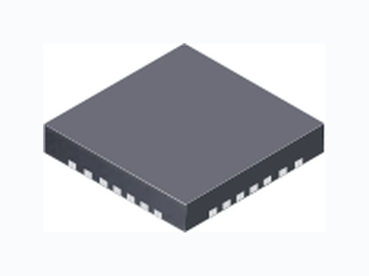
0.68 MF 220 nF C B A C DAC C12 D D VCP1 Charge Pump VPump 100 nF 10 nF C13 100 MF PAD nF 100 100 MF 1 MF 1 MH R8-C11 network is needed only when high inductive load is applied, such as ProBrand LNB. Channel 1 of 2 channels shown. B C D A D3 and D4 are used for surge protection. Either C12 or C9 should be used, but not both. Features and Benefits ▪ 2-wire serial I 2C™ -compatible interface: control (write) and status (read) ▪ LNB voltages (16 programmable levels) compatible with all common standards ▪ Tracking switch-mode power converter for lowest dissipation ▪ Integrated converter switches and current sensing ▪ Output current limit of 900 mA typical, with 48 ms timer ▪ Static current limit circuit allows full current at startup and 13→18 V output transition; reliably starts wide load range ▪ Push-pull output stage minimizes 13 →18 V and 18→13 V output transition times for highly capacitive loads ▪ Adjustable rise/fall time via external timing capacitor ▪ Built-in tone oscillator, factory-trimmed to 22 kHz facilitates DiSEqC™ tone encoding, even at no-load ▪ Four methods of 22 kHz tone generation, via I 2C™ data bits and/or external pin ▪ 22 kHz tone detector facilitates DiSEqC™ 2.0 decoding ▪ Diagnostics for output voltage level, input supply UVLO, and DiSEqC™ tone output ▪ Cable disconnect diagnostic ▪ Auxiliary modulation input ▪ LNB overcurrent with timer Package: 28-pin QFN (suffix ET) 5 mm × 5 mm (Not to scale)
Dual LNB Supply and Control Voltage RegulatorA8286 2Allegro MicroSystems, Inc.
115 Northeast Cutoff, Box 15036
Worcester, Massachusetts 01615-0036 (508) 853-5000 www.allegromicro.com Absolute Maximum Ratings Characteristic Symbol Conditions Rating Units Load Supply Voltage, VIN pin V IN 30 V Output Current1 IOUT Internally Limited A Output Voltage, BOOST pin –0.3 to 33 V Output Voltage, LNB pin Surge2 –1 to 33 V Output Voltage, LX pin –0.3 to 30 V Output Voltage, VCP pin V CP –0.3 to 41 V Logic Input Voltage, EXTM pin –0.3 to 5 V Logic Input Voltage, other pins –0.3 to 7 V Logic Output Voltage –0.3 to 7 V Operating Ambient Temperature T A –20 to 85 °C Junction Temperature T J(max) 150 °C Storage Temperature T stg –55 to 150 °C 1Output current rating may be limited by duty cycle, ambient temperature, and heat sinking. Under any set of conditions, do not exceed the speci- fied current ratings, or a junction temperature, TJ, of 150°C. 2Use Allegro recommended Application circuit. Package Thermal Characteristics* Package RθJA (°C/W) PCB ET 32 4-layer * Additional information is available on the Allegro website.
Ordering Information
Use the following complete part numbers when ordering: Part Number Packing a Description A8286SETTR-Tb 7-in. reel, 1500 pieces/reel 12 mm carrier tape ET package, MLP surface mount aContact Allegro for additional packing options. bLeadframe plating 100% matte tin. A comprehensive set of fault registers are provided which, comply with all the common standards, including: overcurrent, thermal shutdown, undervoltage, cable disconnect, power not good, and tone detect. The device uses a 2-wire bidirectional serial interface, compatible with the I 2C™ standard, that operates up to 400 kHz. The A8286 is supplied in a lead (Pb) free 28-lead MLP/QFN with 100% matte tin leadframe. Description (continued)
Dual LNB Supply and Control Voltage RegulatorA8286 3Allegro MicroSystems, Inc. Worcester, Massachusetts 01615-0036 (508) 853-5000 www.allegromicro.com PAD
22 LNB2
GND – Fused internally; connect to ground plane for thermal dissipation ADD 11 Address select BOOST1 1 Tracking supply voltage to linear regulator (channel 1) BOOST2 21 Tracking supply voltage to linear regulator (channel 2) EXTM1 6 External modulation input (channel 1) EXTM2 16 External modulation input (channel 2) GND 8 Signal ground PAD Pad Exposed thermal pad; connect to ground plane GNDLX1 27 Boost switch ground (channel 1) GNDLX2 23 Boost switch ground (channel 2) IRQ 14 Interrupt request LNB1 28 Output voltage to LNB (channel 1) LNB2 22 Output voltage to LNB (channel 2) LX1 26 Inductor drive point (channel 1) LX2 24 Inductor drive point (channel 2) NC 4, 13, 18 No connection SCL 12 I 2C™-compatible clock input SDA 10 I 2C™-compatible data input/output TCAP1 3 Capacitor for setting the rise and fall time of the LNB output (channel 1) TCAP2 19 Capacitor for setting the rise and fall time of the LNB output (channel 2) TDI1 7 Tone detect input (channel 1) TDI2 15 Tone detect input (channel 2) TDO1 5 Tone detect output (channel 1) TDO2 17 Tone detect output (channel 2) VCP1 2 Gate supply voltage (channel 1) VCP2 20 Gate supply voltage (channel 2) VIN 25 Supply input voltage VREG 9 Analog supply Device Pin-out Diagram (Top View)
Dual LNB Supply and Control Voltage RegulatorA8286 4Allegro MicroSystems, Inc. Worcester, Massachusetts 01615-0036 (508) 853-5000 www.allegromicro.com ELECTRICAL CHARACTERISTICS at TA = 25°C, VIN = 8 to 16 V, unless noted otherwise1 Characteristics Symbol Test Conditions Min. Typ. Max. Units General Set-Point Accuracy, Load and Line Regulation Err Relative to selected VLNB target level, ILOAD = 0 to 500 mA –3 – 3 % Supply Current IIN(Off) ENB bit = 0, LNB output disabled, VIN = 12 V – – 12.0 mA IIN(On) ENB bit = 1, LNB output enabled, ILOAD = 0 mA, VIN = 12 V – – 20.0 mA Boost Switch On Resistance R DS(on)BOOST ILOAD = 500 mA – 300 600 m Ω Switching Frequency f SW 320 352 384 kHz Switch Current Limit I LIMSW VIN = 10 V, VOUT = 20.3 V – 3.8 – A Linear Regulator Voltage Drop ∆VREG VBOOST – VLNB, no tone signal, ILOAD = 500 mA 600 800 1000 mV TCAP Pin Current ICHG TCAP capacitor (C7) charging –12.5 –10 –7.5 μA IDISCHG TCAP capacitor (C7) discharging 7.5 10 12.5 μA Output Voltage Rise Time2 tr(VLNB) For VLNB 13 → 18 V; CTCAP = 5.6 nF, ILOAD = 500 mA – 500 – μs Output Voltage Pull-Down Time2 tf(VLNB) For VLNB 18 → 13 V; CLOAD = 100 μF, ILOAD = 0 mA – 12.5 – ms Output Reverse Current I RLNB ENB bit = 0, VLNB = 33 V , BOOST capacitor (C5) fully charged –1 5 m A Ripple and Noise on LNB Output3 Vrip,n(pp)
20 MHz BWL; reference circuit shown in
Functional Block diagram; contact Allegro for additional information on application circuit board design –3 0 – m V PP Protection Circuitry Output Overcurrent Limit4 ILIMLNB VBOOST – VLNB = 800 mV 800 900 1000 mA Overcurrent Disable Time t DIS 40.0 48 56.0 ms VIN Undervoltage Lockout Threshold V UVLO VIN falling 7.05 7.35 7.65 V VIN Turn On Threshold V IN(th) VIN rising 7.40 7.70 8.00 V Undervoltage Hysteresis V UVLOHYS – 350 – mV Thermal Shutdown Threshold2 TJ – 165 – °C Thermal Shutdown Hysteresis2 ∆TJ –2 0 – ° C Power Not Good Flag Set PNG SET With respect to VLNB 77 85 93 % Power Not Good Flag Reset PNG RESET With respect to VLNB 82 90 98 % Power Not Good Hysteresis PNG HYS With respect to VLNB –5 – % Cable Disconnect Boost Voltage V CAD CADT bit = 1, ENB bit = 1, VSEL0 through VSEL3 = 1 22.0 22.8 23.5 V Cable Disconnect Set V CADSET 20.16 21.00 21.84 V Continued on the next page…
Dual LNB Supply and Control Voltage RegulatorA8286 5Allegro MicroSystems, Inc. Worcester, Massachusetts 01615-0036 (508) 853-5000 www.allegromicro.com Continued on the next page… ELECTRICAL CHARACTERISTICS (continued) at TA = 25°C, VIN = 8 to 16 V, unless noted otherwise1 Characteristics Symbol Test Conditions Min. Typ. Max. Units Tone Tone Frequency f TONE 20 22 24 kHz Tone Amplitude, Peak-to-Peak V TONE(pp) ILOAD = 0 to 500 mA, CLOAD = 750 nF 400 620 800 mV Tone Duty Cycle DC TONE ILOAD = 0 to 500 mA, CLOAD = 750 nF 40 50 60 % Tone Rise Time t rTONE ILOAD = 0 to 500 mA, CLOAD = 750 nF 5 10 15 μs Tone Fall Time t fTONE ILOAD = 0 to 500 mA, CLOAD = 750 nF 5 10 15 μs EXTM Logic Input VEXTM(H) 2.0 – – V VEXTM(L) – – 0.8 V EXTM Input Leakage I EXTMLKG –1 – 1 μA Tone Detector Tone Detect Input Amplitude Receive, Peak-to- Peak V TDR(pp) fTONE = 22 kHz sine wave, TMODE = 0 300 – – mV Tone Detect Input Amplitude Transmit, Peak- to-Peak VTDT(pp)Int fTONE = 22 kHz sine wave, using internal tone (options 1 and 2, in figure 2) 400 – – mV VTDT(pp)Ext fTONE = 22 kHz sine wave, using external tone (options 3 and 4, in figure 2) 300 – – mV Tone Reject Input Amplitude, Peak-to-Peak V TRI(pp) fTONE = 22 kHz sine wave – – 100 mV Frequency Capture f TDI 600 mVpp sine wave 17.6 – 26.4 kHz Input Impedance2 ZTDI – 8.6 – k Ω TDO Output Voltage V TDO(L) Tone present, ILOAD = 3 mA – – 0.4 V TDO Output Leakage I TDOLKG Tone absent, VTDO = 7 V – – 10 μA I2C™-Compatible Interface Logic Input (SDA,SCL) Low Level V SCL(L) – – 0.8 V Logic Input (SDA,SCL) High Level V SCL(H) 2.0 – – V Logic Input Hysteresis V I2CIHYS – 150 – mV Logic Input Current I I2CI VI2CI = 0 to 7 V –10 <±1.0 10 μA Logic Output Voltage SDA and IRQ V t2COut(L) ILOAD = 3 mA – – 0.4 V Logic Output Leakage SDA and IRQ V t2CLKG Vt2COut = 0 to 7 V – – 10 μA SCL Clock Frequency f CLK – – 400 kHz Output Fall Time t fI2COut Vt2COut(H) to Vt2COut(L) – – 250 ns Bus Free Time Between Stop/Start t BUF 1.3 – – μs Hold Time Start Condition t HD:STA 0.6 – – μs Setup Time for Start Condition t SU:STA 0.6 – – μs
Dual LNB Supply and Control Voltage RegulatorA8286 6Allegro MicroSystems, Inc. Worcester, Massachusetts 01615-0036 (508) 853-5000 www.allegromicro.com I2C™-Compatible Interface (continued) SCL Low Time t LOW 1.3 – – μs SCL High Time t HIGH 0.6 – – μs Data Setup Time t SU:DAT 100 – – ns Data Hold Time t HD:DAT For tHD:DAT(min) , the master device must provide a hold time of at least 300 ns for the SDA signal in order to bridge the undefined region of the SCL signal falling edge 0 – 900 ns Setup Time for Stop Condition t SU:STO 0.6 – – μs I2C™ Address Setting ADD Voltage for Address 0001,000 Address1 0 – 0.7 V ADD Voltage for Address 0001,001 Address2 1.3 – 1.7 V ADD Voltage for Address 0001,010 Address3 2.3 – 2.7 V ADD Voltage for Address 0001,011 Address4 3.3 – 5.0 V 1Operation at 16 V may be limited by power loss in the linear regulator. 2Guaranteed by worst case process simulations and system characterization. Not production tested. 3LNB output ripple and noise are dependent on component selection and PCB layout. Refer to the Application Schematic and PCB layout recommendations. Not production tested. 4Current from the LNB output may be limited by the choice of Boost components. SDA SCL tSU:STA tHD:STA tSU:DAT tHD:DAT tBUF tSU:STO tHIGH tLOW I2C™ Interface Timing Diagram ELECTRICAL CHARACTERISTICS (continued) at TA = 25°C, VIN = 8 to 16 V, unless noted otherwise1 Characteristics Symbol Test Conditions Min. Typ. Max. Units
Dual LNB Supply and Control Voltage RegulatorA8286 7Allegro MicroSystems, Inc. Worcester, Massachusetts 01615-0036 (508) 853-5000 www.allegromicro.com Protection The A8286 has a wide range of protection features and fault diag- nostics which are detailed in the Status Register section. Boost Converter/Linear Regulator Each channel contains a tracking current-mode boost converter and linear regulator. The boost converter tracks the requested LNB voltage to within 800 mV , to minimize power dissipation. Under conditions where the input voltage, V BOOST , is greater than the output voltage, VLNB, the linear regulator must drop the dif- ferential voltage. When operating in these conditions, care must be taken to ensure that the safe operating temperature range of the A8286 is not exceeded. The A8286 has internal pulse-by-pulse current limit on the boost converter, and DC current limiting on the LNB output, to protect the IC against short circuits. When the LNB output is shorted, the LNB output current is limited to 900 mA typical, and the IC will be shut down if the overcurrent condition lasts for more than 48 ms. If this occurs, the A8286 must be re-enabled for normal opera- tion. The system should provide sufficient time between successive restarts to limit internal power dissipation; a period of 5 s is recom- mended. Each of the boost converters operates at 352 kHz typical: 16 times the internal 22 kHz tone frequency. All the loop compen- sation, current sensing, and slope compensation functions are pro- vided internally. At extremely light loads, and the boost converters operate in a pulse-skipping mode. Pulse skipping occurs when the BOOST voltage rises to approximately 450 mV above the BOOST target output voltage. Pulse skipping stops when the BOOST voltage drops 200 mV below the pulse skipping level. In the case that two or more set top box LNB outputs are con- nected together by the customer (e.g., with a splitter), it is possible that one output could be programmed at a higher voltage than the other. This would cause a voltage on one output that is higher than its programmed voltage (e.g., 19 V on the output of a 13 V pro- grammed voltage). The output with the highest voltage will effec- tively turn off the other outputs. As soon as this voltage is reduced below the value of the other outputs, the A8286 output will auto- recover to their programmed levels. Charge Pump. Each generates a supply voltage above the internal tracking regulator output to drive the linear regulator control. Slew Rate Control. During either start-up, or when the output voltage at the LNB pin is transitioning, the output voltage rise and fall times can be set by the value of the capacitor connected from the TCAP1 pin to GND (C TCAP or C7 in the Applications Sche- matic). Note that during start-up, the BOOST pin is pre-charged to the input voltage minus a voltage drop. As a result, the slew rate control for the BOOST pin occurs from this voltage. The value of C TCAP can be calculated using the following for- mula: CTCAP = (ITCAP × 6) / SR , where SR is the required slew rate of the LNB output voltage, in V/s, and ITCAP is the TCAP pin current specified in the data- sheet. The recommended value for CTCAP, 10 nF, should provide satisfactory operation for most applications. However, in some cases, it may be necessary to increase the value of C TCAP to avoid activating the current limit of the LNB output. One such situation is when two set-top boxes are connected in parallel. If this is the case, the following formula can be used to calculate a larger value for C TCAP: C TCAP ≥ (ITCAP × 6)(2 × CBOOST) / ILIMLNB , C TCAP ≥ (10 μA × 6)(2 × 100 μF) / 800 mA = 15 nF . The minimum value of CTCAP is 2.2nF. There is no theoretical maximum value of CTCAP , however, too large a value will proba- bly cause the voltage transition specifications to be exceeded. Tone generation is unaffected by the value of C TCAP. Pull-Down Rate Control. In applications that have to operate at very light loads and that require large load capacitances (in the order of tens to hundreds of microfarads), the output linear stage provides approximately 40 mA of pull-down capability. This ensures that the output volts are ramped from 18 V to 13 V in a reasonable amount of time. Functional Description
5 s of delay between restarts. Table 1. Detection Thresholds for Tone Generation Options Figure 1. ODT (Overcurrent Disable Timing) Mode Timing Diagram
the tone source is either internal or external (via the EXTM pin). trol, whether gated or clocked. grammed voltage minus 325 mV (typical). tone detection amplitude is 300 mV . to access the internal Control and Status registers of the A8286. depending on the direction of the data.
- Start Condition. Defined by a negative edge on the SDA line,
- Address Cycle. 7 bits of address, plus 1 bit to indicate read (1)
fined by the remaining two bits, are selected by the ADD input. The address is transmitted MSB first. Register section for more information.
- Stop Condition. Defined by a positive edge on the SDA line,
Option 1 – Use internal tone, gated by the TGATE bit. Option 2 – Use internal tone, gated by the EXTM pin. Option 3 – Use external tone, gated by the TGATE bit. Option 4 – Use external tone. Figure 2. Options for tone generation
10Allegro MicroSystems, Inc. A8286 always responds by resetting the data transfer sequence. write operations must be preceded with the address. cycle, in order to allow this handshaking to occur. of the SDA line and send the data from register 1 to the master. Figure 3. I2C™ Interface. Read and write sequences.
11Allegro MicroSystems, Inc. section for full description. or due to a fault, or is enabled. status register to determine which device is requesting attention. that the A8286 is fully active with no fault conditions. Figure 4. I2C™ Interface. Read sequences after interrupt request.
12Allegro MicroSystems, Inc. states for the control functions are all 0s. Table 2. Control Registers with Address (I1, I0) = 00 and 01
0 VSEL 01 VSEL 02
2 VSEL 21 VSEL 22
3 VSEL 31 VSEL 32 0: LNBx = Low range
4 ODT1 ODT2 1 (recommended): The ODT functions are always
enabled, but setting 1 recommended at all times.
5 ENB1 ENB2 0: Disable LNBx Output
Bit 0 VSEL 0x These three bits provide incremental control over the voltage on the LNB x output. defined in table 4, Output V oltage Amplitude Selection. 2x, VSEL1x and VSEL0x control register bits. Bit 4 ODT x The overcurrent disable timers are always enabled. the LNBx output is disabled.
13Allegro MicroSystems, Inc. Table 3. Control Registers with Address (I1, I0) = 10 and 11
0 TMODE1 TMODE2 0: External Tone
1 TGATE1 TGATE2 0: Tone Gated Off
2 CADT1 CADT2 0: Cable Disconnect Test Off
6 I0 I0
7 I1 I1
of the internal 22 kHz oscillator to control the tone generation on the LNBx output. connected and the CAD bit in the Status register is set to 0.
14Allegro MicroSystems, Inc. Table 4. Output Voltage Amplitude Selection
15Allegro MicroSystems, Inc. master, assuming the fault has been resolved. performed, register 1 is always read first. registers is all 0s, to simplify checking of the Status bit. Table 5. Status Register Bit Setting
16Allegro MicroSystems, Inc. Table 6. Status Register 1
0 DIS1 LNB output disabled (Channel 1)
1 DIS2 LNB output disabled (Channel 2)
2 OCP1 Overcurrent (Channel 1)
3 OCP2 Overcurrent (Channel 2)
4 PNG1 Power Not Good (Channel 1)
5 PNG2 Power Not Good (Channel 2)
6 TSD Thermal Shutdown
7 VUV V
write sequence if the LNB output is enabled. Bit 1 DIS2 See description for DIS1. This indicates status for channel 2. the OCP bit is reset in all cases, allowing the master to reenable the LNB output. Bit 3 OCP1 See description for OCP1. This indicates status for channel 2. output is enabled and within 90% of the programmed LNB voltage. Bit 5 PNG2 See description for PNG1. This indicates status for channel 2. required. If the condition is still present, then the TSD bit will remain at 1. output if required. If the condition is still present, then the VUV bit will remain at 1.
17Allegro MicroSystems, Inc. Table 7. Status Register 2
0 CAD1 Cable Disconnected (Channel 1)
1 CAD2 Cable Disconnected (Channel 2)
2 TDET1 Tone Detect (Channel 1)
3 TDET2 Tone Detect (Channel 2)
Bit 1 CAD2 See description for CAD1. This indicates status for channel 2. the tone is disabled and no tone is received from the LNB, TDET1 is reset. Bit 3 TDET2 See description for CAD1. This indicates status for channel 2.
18Allegro MicroSystems, Inc. Table 8. Component Selection Tablea aComponents for channel 1 and channel 2 are identical. bEither C9 or C12 are used, but not both.
Dual LNB Supply and Control Voltage RegulatorA8286 19Allegro MicroSystems, Inc. Worcester, Massachusetts 01615-0036 (508) 853-5000 www.allegromicro.com 0.25 +0.05 –0.07 0.55 +0.20 –0.10 0.50 0.90 ±0.10 C0.08 29X SEATING PLANE C A Terminal #1 mark area B Exposed thermal pad (reference only, terminal #1 identifier appearance at supplier discretion) For Reference Only (reference JEDEC MO-220VHHD-1) Dimensions in millimeters Exact case and lead configuration at supplier discretion within limits shown C Reference land pattern layout (reference IPC7351 QFN50P500X500X100-29V1M); All pads a minimum of 0.20 mm from all adjacent pads; adjust as necessary to meet application process requirements and PCB layout tolerances; when mounting on a multilayer PCB, thermal vias at the exposed thermal pad land can improve thermal dissipation (reference EIA/JEDEC Standard JESD51-5) A PCB Layout Reference View B 3.15 3.15 3.15 3.15 0.30 28 0.501.15 4.80 4.80 C 5.00 ±0.15 5.00 ±0.15 D D Coplanarity includes exposed thermal pad and terminals Package ET 28-Pin MLP/QFN
Dual LNB Supply and Control Voltage RegulatorA8286 20Allegro MicroSystems, Inc. Worcester, Massachusetts 01615-0036 (508) 853-5000 www.allegromicro.com I2C™ is a trademark of Philips Semiconductors. DiSEqC™ is a trademark of Eutelsat S.A. For the latest version of this document, visit our website: www.allegromicro.com Allegro MicroSystems, Inc. reserves the right to make, from time to time, such de par tures from the detail spec i fi ca tions as may be required to permit improvements in the per for mance, reliability, or manufacturability of its products. Before placing an order, the user is cautioned to verify that the information being relied upon is current. Allegro’s products are not to be used in life support devices or systems, if a failure of an Allegro product can reasonably be expected to cause the failure of that life support device or system, or to affect the safety or effectiveness of that device or system. The in for ma tion in clud ed herein is believed to be ac cu rate and reliable. How ev er, Allegro MicroSystems, Inc. assumes no re spon si bil i ty for its use; nor for any in fringe ment of patents or other rights of third parties which may result from its use. Copyright ©2005-2012, Allegro MicroSystems, Inc.
Revision History
Revision Revision Date Description of Revision Rev. 17 February 15, 2012 Absolute Maximum Ratings