
DATASHEET SEARCH SITE
Document overview
- Manufacturer or author: Provided By www.digicamel.com(FREE DATASHEET DOWNLOAD SITE)
- PDF pages: 12
Technical content
Description
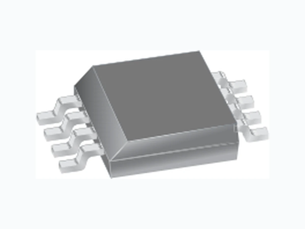
The Allegro ® A6850 is designed to interface between a microprocessor and a pair of 2-wire Hall effect sensor ICs. The A6850 uses protected high-side low resistance DMOS MOSFETs to switch the supply voltage to the two Hall effect devices. Each switch can be controlled independently via individual ENABLE pins and both switches are protected with current-limiting circuitry. The output switches are rated to operate to 26.5 V and will source at least 25 mA per channel before current limiting. Typical two-wire Hall device applications require the user to measure the supply current to determine whether the Hall IC is switched on (magnetic field present) or switched off (no magnetic field present). This is usually accomplished by using an external series shunt resistor and protection circuits for the microprocessor. In many systems, the sensed voltage is used as the input to a microprocessor analog-to-digital (A-to-D) input. This provides the system with an indication of the status of the two-wire switch as well as provides the capability for diagnostic information if there is an open or shorted Hall device. Approximate Scale 1:1 6850-DS Rev. 5 Features and Benefits ▪ 4.75 to 26.5 V operation ▪ Low V IN-to-VOUT voltage drop ▪ 1/10 current sense feedback ▪ Survive short-to-battery and short-to-ground faults ▪ Survive 40 V load dump ▪ >4 kV ESD rating on the output pins, >2 kV on all other pins ▪ Output current limiting ▪ Low operating and Sleep mode currents ▪ Integrates with Allegro A114x and A118x Hall effect two-wire sensor ICs Dual Channel Switch Interface IC Continued on the next page… Package: 8 pin SOIC (suffix L) Functional Block Diagram A6850 VIN OUTPUT1 GROUND SENSE1 ENABLE1 ENABLE2 OUTPUT2 SENSE2 Fault Detection Control Block IOUTPUT1×1/10 Fault Detection IOUTPUT2×1/10
Dual Channel Switch Interface ICA6850 2Allegro MicroSystems, Inc.
115 Northeast Cutoff
Worcester, Massachusetts 01615-0036 U.S.A. Terminal List Table Name Number Description ENABLE1 1 Digital input pulled to ground SENSE1 2 Sensed current output ENABLE2 3 Digital input pulled to ground SENSE2 4 Sensed current output VIN 5 Chip power supply voltage OUTPUT2 6 Switchable voltage supply to sensor IC GROUND 7 Ground reference OUTPUT1 8 Switchable voltage supply to sensor IC 8ENABLE1 SENSE1 ENABLE2 SENSE2 OUTPUT1 GROUND OUTPUT2 VIN Switch Switch Control The A6850 eliminates the need for the external series shunt resistor in Hall device applications by incorporating an integrated current mirror which reports the Hall IC supply current as a 1/10 value on the SENSE1 or SENSE2 output pin. A low current Sleep mode is available (<15 μA) by driving both ENABLE pins low. Also, the A6850 can be used to interface to mechanical switches. The A6850 is supplied in an 8-pin Pb (lead) free SOIC package, with 100% matte tin leadframe plating. Description (continued) Pin-out Diagram Selection Guide Part Number Packing A6850KLTR-T 13-in. reel, 3000 pieces/reel Absolute Maximum Ratings Characteristic Symbol Notes Rating Units Supply Voltage V IN 40 V Output Voltage V OUTPUTx –0.3 to 40 V SENSEx Voltage Range V SENSEx –0.3 to 7 V ENABLEx Voltage Range V ENABLEx –0.3 to 7 V Operating Ambient Temperature T A –40 to 150 ºC Maximum Junction Temperature T J(max) 150 ºC Storage Temperature T stg –55 to 150 ºC ESD Rating - Human Body Model HBM AEC-Q100-002; OUTPUT1 and OUTPUT2 4.5 kV AEC-Q100-002; all other pins 2.5 kV ESD Rating - Charged Device Model CDM AEC-Q100-011; all pins 1050 V THERMAL CHARACTERISTICS may require derating at maximum conditions, see application information Characteristic Symbol Test Conditions* Value Units Package Thermal Resistance R θJA 4-layer PCB based on JEDEC standard 80 ºC/W 1-layer PCB with copper limited to solder pads 140 ºC/W *Additional thermal data available on the Allegro Web site.
Dual Channel Switch Interface ICA6850 3Allegro MicroSystems, Inc. Worcester, Massachusetts 01615-0036 U.S.A. ELECTRICAL CHARACTERISTICS at TJ = -40 to +150°C (unless noted otherwise) Characteristics Symbol Test Conditions Min. Typ. Max. Units Supply Input Voltage Range V IN 4.75 – 26.5 V Supply Input Quiescent Current I INQ Operating mode, IOUTPUTx = 0 mA – – 5.0 mA Sleep mode: ENABLE1 and ENABLE2 low V OUTPUT1 = VOUTPUT2 = 0 V ––1 5 μA Power-Up Time1 tON ––2 0 μs Output Rise Time2 trLH IOUTPUTx = 0 to –10 mA, 10% to 90%VSENSEx – 0.18 1.5 μs Output Fall Time2 tfHL IOUTPUTx = 0 to –10 mA, 90% to 10%VSENSEx – 1.4 3.5 μs Enable Delay Time2 tENdlyLH IOUTPUTx = –5 mA, 50% ENABLEx to 50%VSENSEx – 150 500 ns Disable Delay Time2 tENdlyHL IOUTPUTx = –5 mA, 50% ENABLEx to 50%VSENSEx – 4.0 7.5 μs OUTPUTx Source Resistance R DS(on) IOUTPUTx = –20 mA – – 35 Ω OUTPUTx Leakage Current I OUTPUTQ VOUTPUTx = 0 V; disabled – – –20 μA SENSEx Output Current Offset3 ISENSE(ofs) ISENSEx = (IOUTPUTx / 10) + ISENSE(ofs), IOUTPUT = –2 mA to –20 mA –100 – 100 μA ISENSEQ VSENSEx = 0 V; disabled – – 10 μA SENSEx Voltage4 VSENSEx VIN > 7 V 0 – 6 V VIN < 7 V 0 – V IN – 1 V ENABLEx Input Voltage Range VENABLEH 2.0 – – V VENABLEL – – 0.4 V ENABLEx Input Hysteresis V ENABLEhys At least one output enabled 125 – 375 mV ENABLEx Current I ENABLE ENABLEx = 2.0 V – 40 100 μA ENABLEx = 0.4 V – 8.0 20 μA OUTPUT Current Limit I OUTPUTM –25.0 –35.0 –45.0 mA OUTPUT Reverse Bias Current I OUTPUT(rvrs) Reverse bias blocking: VIN = 4.75 V, VOUTPUT = 26.5 V – 500 750 μA Overvoltage Protection Threshold V OVP Rising VIN 27.0 – 33.0 V Overvoltage Protection Hysteresis V OVPhys – 2.0 – V Thermal Shutdown Threshold T TSD Temperature Increasing – 175 – °C Thermal Shutdown Hysteresis T TSDhys –1 5 – ° C 1Delay from end of Sleep mode to outputs enabled. 2 RSENSEx = 1.5 kΩ. 3For input and output current specifications, negative current is defined as coming out of (sourced from) the specified device pin. 4User to ensure that VSENSEx remains within the specified range. If VSENSEx exceeds the maximum value, the device is self-protected by an internal clamp, but not all parameters perform as specified.
Worcester, Massachusetts 01615-0036 U.S.A. Figure 2. Enable Delays, one ENABLE input held high to prevent the IC going into Sleep mode Figure 1. Signal Channel Timing, ENABLE1 = ENABLE1 = High, RSENSE = 1.5 kΩ
Worcester, Massachusetts 01615-0036 U.S.A. be translated onto the SENSE pins. on the sense pin (see Electrical Characteristics table). tion section for schematic diagrams and power calculations. current is shunted to ground and does not appear on the VIN pin. overvoltage threshold, VOVP , the A6850 will shut off the outputs. switch with hysteresis until the regulators stabilize. ENABLE pin is held high, the A6850 operates with hysteresis. Figure 3. Activation Timing Diagram. Exiting Sleep mode via ENABLE
Worcester, Massachusetts 01615-0036 U.S.A. transfer characteristic can be considered that of a low pass filter. Characteristic Performance section. The result is in MHz when trLH is in ns. The result is in MHz when trLH and tfHL are in ns. their respective ENABLEx pins, as shown in table 1. current limit value for the OUTPUTx pins. usually cause a signal overshoot as shown as tENsettle in figure 4. the TSD hysteresis, TTSDhys. Table 1. Enable/Disable Signal Channel Truth Table Figure 4. Overshoot resulting from additional capacitance.
Dual Channel Switch Interface ICA6850 7Allegro MicroSystems, Inc. Worcester, Massachusetts 01615-0036 U.S.A. TJ can be estimated by calculating the power dissipation (PD) of the A6850. To calculate PD: PD = VIN IINQ (6) – VOUTPUT1 IOUTPUT1 – VOUTPUT2 IOUTPUT2 – VSENSE1 ISENSE1 – VSENSE2 ISENSE2 . PD = VIN IINQ (7) + ( VIN – VOUTPUT1 ) IOUTPUT1 + ( VIN – VOUTPUT2 ) IOUTPUT2 + ( VIN – VSENSE1) ISENSE1 + ( VIN – VSENSE2) ISENSE2 . When IOUTPUTx × RDS(on) < approximately 700 mV , then: (V IN – VOUTPUTx ) = IOUTPUTx × RDS(on) . When IOUTPUTx × RDS(on) > approximately 700 mV , then: I OUTPUTx = IOUTPUT (max) , and VOUTPUTx is set by the loading on the OUTPUTx pin. The temperature rise of the A6850 can be calculated by multiply- ing PD and the thermal resistance from junction to ambient, RθJA . The formula for temperature rise, ΔT, is: ΔT = PD × RθJA . (8) The RθJA for an 8-pin SOIC (Allegro L package) on a one-layer board with minimum copper area is 140 °C/W. (More thermal data is available on the Allegro MicroSystems website.) The total junction temperature can be calculated by: T J = TA + ΔT , (9) where TA is the ambient air temperature. Example: Calculating the power dissipation and temperature rise, given: T A = 25°C , V IN = 5 V , I INQ = 5 mA , I OUTPUT1 = IOUTPUT2 = 15 mA , I SENSEx = IOUTPUTx /10 = 1.5 mA , R SENSE1 = RSENSE2 = 2 kΩ , and IOUTPUTx × RDS(on) = 15 × 35 = 525 mV = VIN – VOUTPUTx . Then: P D = 5 V × 5 mA = 46.75 mW . Substituting in equation 8: Substituting in equation 9:
Worcester, Massachusetts 01615-0036 U.S.A. within these ranges indicates a fault condition. conditions that can be monitored through the SENSE pins. *This current range includes all A114x and A118x devices. Figure 5. Typical Application with 2-Wire Hall Effect ICs
Worcester, Massachusetts 01615-0036 U.S.A. sipation in the OUTPUTx section of the A6850. Figure 6. Typical Application with Mechanical Switches
10Allegro MicroSystems, Inc. Worcester, Massachusetts 01615-0036 U.S.A. SENSEx remain within specification. Figure 7. Outline of ganged configuration Figure 8. Functional response in ganged configuration
11Allegro MicroSystems, Inc. Worcester, Massachusetts 01615-0036 U.S.A. to the VIN and GND pins as feasible. results should be validated. Figure 9. Decoupling and filtering suggestions
Dual Channel Switch Interface ICA6850 12Allegro MicroSystems, Inc. Worcester, Massachusetts 01615-0036 U.S.A. L Package, 8-Pin SOIC CSEATING PLANE
1.27 BSC
A A Terminal #1 mark area B Reference land pattern layout (reference IPC7351 SOIC127P600X175-9AM); all pads a minimum of 0.20 mm from all adjacent pads; adjust as necessary to meet application process requirements and PCB layout tolerances; when mounting on a multilayer PCB, thermal vias at the exposed thermal pad land can improve thermal dissipation (reference EIA/JEDEC Standard JESD51-5) PCB Layout Reference View B
1.75 MAX
C 0.65 1.27 5.60 1.75 C0.20
0.25 BSC
(1.04) For Reference Only, not for tooling use (reference JEDEC MS-012 AA) Dimensions in millimeters Dimensions exclusive of mold flash, gate burrs, and dambar protrusions Exact case and lead configuration at supplier discretion within limits shown 4.90 ±0.10 3.90 ±0.10 0.41 ±0.10 6.00 ±0.20 0.21 ±0.04 4° ±4 0.84 +0.43 –0.44 0.18 +0.08 –0.07 For the latest version of this document, visit our website: www.allegromicro.com Copyright ©2006-2011, Allegro MicroSystems, Inc. Allegro MicroSystems, Inc. reserves the right to make, from time to time, such de par tures from the detail spec i fi ca tions as may be required to per- mit improvements in the per for mance, reliability, or manufacturability of its products. Before placing an order, the user is cautioned to verify that the information being relied upon is current. Allegro’s products are not to be used in life support devices or systems, if a failure of an Allegro product can reasonably be expected to cause the failure of that life support device or system, or to affect the safety or effectiveness of that device or system. The in for ma tion in clud ed herein is believed to be ac cu rate and reliable. How ev er, Allegro MicroSystems, Inc. assumes no re spon si bil i ty for its use; nor for any in fringe ment of patents or other rights of third parties which may result from its use.