
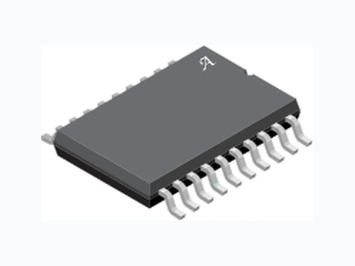
A6274 ALLEGRO
Document overview
- Manufacturer or author: Provided By www.digicamel.com(FREE DATASHEET DOWNLOAD SITE)
- PDF pages: 24
Technical content
The A6274 and A6284 are programmable linear current regulator ICs for driving automotive LED arrays. The LED current is programmed by external resistors. These devices sink up to 60 mA (A6274) or 120 mA (A6284), from each of six LED pins, to drive strings of high-brightness LEDs. LED pins can be paralleled to drive even higher current LED strings. Current settings are typically accurate to 2%, while typical matching between LED strings is 0.8%. LED light output can be adjusted by PWM dimming. The ICs provide an internal PWM dimming circuit that is programmed by external resistors for PWM frequency and duty cycle. It can also accept an external PWM signal. Multiple ICs can be configured in parallel for larger lighting systems. An internal FULL (V DR > 3.6 V) option is provided to override the PWM- dimming ratio for full LED current. LED current derating with temperature and programmable VIN levels allows operation over a wide range of operating conditions. A6274-84-DS, Rev. 1
- Six LED current sinks rated up to 60 mA (A6274) or 120 mA (A6284)
- Total LED drive current—up to 360 mA or 720 mA
- Wide input voltage range of 5 to 42 V for start/stop, cold- crank, and load-dump requirements
- Low-dropout voltage—drives two series WLEDs from 7 V input
- Gate driver for external ballast P-MOSFET
- LEDs combined in two groups with separate ENx and ISETx LED current level set by external reference resistors
- Internal or external PWM dimming
- Controlled output drivers slew during PWM for lower EMI Fault detection features: LED string open, LED pin short-to-ground, single LED short, VOUT short-to- ground, VIN overvoltage, and thermal protection
- Input supply and temperature-based derating
- Automotive K-temperature range (–40°C to 150°C) Linear Current Regulator and Controller for Automotive LED Arrays PACKAGES: Not to scale A6274, A6274-1 A6284, A6284-1 FEATURES AND BENEFITS DESCRIPTION 20-Pin eTSSOP (LP) with Exposed Thermal Pad AEC-Q100 qualified Continued on next page...
APPLICATIONS
- Automotive rear combination light
- DRL/position
- General automotive lighting Figure 1: Typical Application Diagram for “-1” Latching V ersion C3 C4C2 GATE VIN EN1 EN2 BIAS VTH FFn DR PWMIN ISET1 ISET2 GND LED6 LED5 LED4 LED3 LED2 LED1 OUTCOMP A6274-84 DIM FULL FFn EN2 EN1
Linear Current Regulator and Controller for Automotive LED Arrays A6274, A6274-1 A6284, A6284-1 Allegro MicroSystems, LLC
115 Northeast Cutoff
Worcester, Massachusetts 01615-0036 U.S.A. ABSOLUTE MAXIMUM RATINGS 3 Characteristic Symbol Notes Rating Unit VIN, OUT, DR, EN1, EN2, COMP, FFn VIN, VOUT, VCOMP, VDR, VEN1, VEN2, VFFn −0.3 to 45 V GATE VGATE Max of (–0.3 or VIN – 9) to 45 V LED1 to LED6 VLEDx −0.5 to 45 V All other pins −0.3 to 6.5 V Junction Temperature TJ −40 to 150 °C Transient Junction Temperature TJt Overtemperature event not exceeding 10 seconds, lifetime duration not exceeding 10 hours, determined by design characterization. 175 °C Storage Temperature Range T stg −55 to 150 °C 3 Stresses beyond those listed in this table may cause permanent damage to the device. The absolute maximum ratings are stress ratings only, and functional operation of the device at these or any other conditions beyond those indicated in the Electrical Characteristics table is not implied. Exposure to absolute-maximum-rated conditions for extended periods may affect device reliability. THERMAL CHARACTERISTICS Characteristic Symbol Test Conditions4 Value Unit Junction-to-Ambient Thermal Resistance RθJA Estimated, on 4-layer PCB based on JEDEC standard 29 °C/W 4 Additional thermal information available on the Allegro website. SELECTION GUIDE Part Number ILED(MAX) FAULT Response (see Table 2 for details) Package Packing1 A6274KLPTR-T 60 mA per channel Unlatched MODE0 20-pin eTSSOP with thermal pad 4,000 pieces per 13-in. reel A6284KLPTR-T 120 mA per channel Unlatched MODE0 A6274KLPTR-1-T 60 mA per channel Latched MODE1 A6284KLPTR-1-T 120 mA per channel Latched MODE1 1 Contact Allegro™ for additional packing options. SPECIFICATIONS A GATE pin is provided to drive an external P-channel MOSFET, which serves as an active ballast resistor to reduce the heat dissipation within the IC package. It also serves as an input disconnect switch in the event of an LED string short-to-ground fault. The A6274 and A6284 provide a non-latching option while the A6274-1 and A6284-1 provide a latching option. DESCRIPTION (continued)
Linear Current Regulator and Controller for Automotive LED Arrays A6274, A6274-1 A6284, A6284-1 Allegro MicroSystems, LLC Worcester, Massachusetts 01615-0036 U.S.A. Package LP, 20-Pin eTSSOP Pinout Diagram Terminal List Table Number Symbol Function
1 ISET1
Sets LEDx sink current for LED1-3. Connect resistor to GND to set current, up to 60 mA (A6274) or 120 mA (A6284) per channel. ISET2 Sets LEDx sink current for LED4-6. Connect resistor to GND to set current, up to 60 mA (A6274) or 120 mA (A6284) per channel. Connect ISET2 to BIAS if only one resistor setting is required for LED1-6.
3 VTH
Sets input voltage threshold for current foldback and V OUT threshold for open-LED fault (D, E, F, and G) disable threshold.
4 PWMIN
PWM frequency setting. Internal PWM frequency set when connected to GND through a resistor and uses external PWM when a logic signal is applied to this pin.
5 BIAS
Output of internal bias regulator. Connect a µF decoupling capacitor near to IC pin. BIAS pin can deliver up to 7 mA to an external load. FFn Active-low fault flag. This pin can be used as an input pin while using “-1” latching version. If pulled low, IC will turn all LEDs off for one-out- all-out functionality across multiple chips in the system. 7, 8, 9 LED1-3 Three LED current sinks. Connect the cathode of each LED string to these pins. 10 GND Ground pin. 11, 12, 13 LED4-6 Three LED current sinks. Connect the cathode of each LED string to these pins. 14 OUT Connect to drain of series-pass MOSFET.
15 COMP
nF capacitor across COMP pin and drain node of external PMOS. If PMOS is not used, connect this pin to VIN. GATE Gate drive for series-pass MOSFET. If PMOS is not used, connect this pin to VIN.
17 VIN
Input voltage to IC. Connect to source of series- pass P-channel MOSFET. Connect a decoupling capacitor close to this pin. 18 EN1 Active-high-enable input for LED1-3. 19 EN2 Active-high-enable input for LED4-6. 20 DR Voltage on this pin sets dimming duty cycle when 0 < V DR < 3.6 V. IC operates with 100% duty cycle in internal and external PWM mode when V DR > VDRDC(max) – PAD Thermal pad. Solder to ground plane for better thermal performance. ISET1 ISET2 VTH PWMIN BIAS FFn LED1 LED2 LED3 GND LED4 LED5 LED6 OUT COMP GATE VIN EN1 EN2 DR1 10 11 PAD PINOUT DIAGRAM AND TERMINAL LIST TABLE
Linear Current Regulator and Controller for Automotive LED Arrays A6274, A6274-1 A6284, A6284-1 Allegro MicroSystems, LLC Worcester, Massachusetts 01615-0036 U.S.A. Functional Block Diagram LDOVBIAS EN1 EN1 EN2 EN2 VTH DR PWMIN ISET2 ISET1 FFn GND LED6 LED5 LED4 LED3 LED2 LED1 VING ATEC OMPO UT FULL ON/OFF EN1 EN2 OUTS hort V OUTS hort Fault Driver Reference Current Internal PWM Generator Feedback and Control LED Open/ Short Detect A6274-84 TSD
Linear Current Regulator and Controller for Automotive LED Arrays A6274, A6274-1 A6284, A6284-1 Allegro MicroSystems, LLC Worcester, Massachusetts 01615-0036 U.S.A. Characteristics Symbol Test Conditions Min. Typ. Max. Unit INPUT SPECIFICATIONS Operating Input Voltage Range VIN ● 5 – 42 V Input Quiescent Current 1 IQ VENx = high, FULL mode – – 6 mA Input Sleep Supply Current 1 IQSLEEP VEN1 = VEN2 = 0 V; VDR = VBIAS ● – – 6 μA INTERNAL BIAS CIRCUIT BIAS Pin Voltage V BIAS IBIAS = 0 to 7 mA, 5.6 V ≤ VIN ≤ 18 V ● 4.75 5 5.25 V BIAS Pin Dropout VBIASDROP Minimum voltage drop across VIN and BIAS pins. IBIAS < 7 mA, VIN = 5 V – 0.3 – V VBIAS Undervoltage Release Threshold VBIASSTART VIN rising ● – – 4.6 V VBIAS Undervoltage Lockout Stop Threshold VBIASSTOP VIN falling ● – – 4.2 V P-CHANNEL MOSFET DRIVER SPECIFICATION GATE Sink Current 1 IGATE(SINK) Due to on-chip current limit, 10 V < VIN < 18 V 4 – – mA Due to on-chip current limit, VIN = 5 V 2 – – mA GATE Maximum Voltage (w .r.t. VIN) VGATE(MAX) VIN – VGATE, VLEDx = 0.3 V 8 10 12 V GATE Minimum Voltage (w .r.t. VIN) VGATE(MIN) VIN – VGATE, VLEDx = 1 V – 130 360 mV PMOS Detect Threshold VGATE(PMOS) Voltage measured (VIN – VGATE) at end of startup to detect PMOS connected – 600 – mV LEDx CURRENT DRIVER SPECIFICATION LEDx Regulation Voltage 2a VLEDreg A6274; not in derating ● – 0.4 0.7 V A6284; not in derating ● – 0.55 0.85 V LEDx Accuracy 3 ErrLEDx Measured at ILED(MAX), LEDx mismatch < 0.5 V, 5 V < VIN < 18 V, TJ = 0°C to 150°C – 2 3.5 % LEDx Matching 4 ΔILEDx ISET2 connected to BIAS; compared to average ILEDx, measured at ILED(MAX), LEDx mismatch < 1 V, 5 V < VIN < 18 V
- – 0.8 3 % Maximum LEDx Current ILED(MAX) A6274 ● – 60 – mA A6284 ● – 120 – mA Minimum LEDx Current ILED(MIN) A6274 – 6 – mA A6284 – 12 – mA Maximum LED Current, ISETx Pin Short-to- Ground 2 ILED(ISETshrt) A6274 – 66 – mA A6284 – 129 – mA LED Current Ramp Time tRAMP ILEDx 10% to 90% and 90% to 10% – 8 – μs ISETx to ILEDx Gain gILED A6274 – 248 – A/A A6284 – 492 – A/A ISETx Voltage Level VISET 0.015 mA ≤ IISETx ≤ 0.3 mA – 1.2 – V Continued on the next page… ELECTRICAL CHARACTERISTICS: Valid at VIN = 14 V, VENx = 3.3 V; ● indicates specifications across the full operating temperature range with TJ = –40°C to 150°C; other specifications are at TJ = 25°C, unless noted otherwise. Refer to Figure 1 for typical application circuit.
Linear Current Regulator and Controller for Automotive LED Arrays A6274, A6274-1 A6284, A6284-1 Allegro MicroSystems, LLC Worcester, Massachusetts 01615-0036 U.S.A. Characteristics Symbol Test Conditions Min. Typ. Max. Unit PROTECTION VIN Required to Derate ILED by 10% VINth(L) VVTH = 1.84 V 19 20 21 V VIN Derating Range (VINth(L) to VINth(H)) VINthd ILED drops from 90% to 50% level – 6.4 – V MOSFET Drain Short Protection Threshold VOUT(SC) Measure across OUT and GND pins – 1 – V MOSFET Drain Short Protection Blank Delay t d(OUT,scblnk) Protection disabled from enable instance – 1 – ms String Short Detect Voltage VSC(STRING) While LED sinks are in regulation; sensed from VLEDx to VLEDreg, 5 V < VIN < 18 V 1.8 – 2.6 V LEDx Not-In-Use Voltage VLEDx(NULL) Detect during tLEDdet time period 0.18 0.26 0.34 V LEDx Pin Source Current ILEDsrc Source current for Not-In-Use Detection 65 – 95 μA LED Connected Detect Time tLEDdet ENx = high and VGATE ≤ (VIN – 3.3) at startup – 5 – ms LEDx Short-to-Ground Detect Voltage VLED(SC) − − 0.16 V Open-LED Disable Voltage VOLED_dis Measured at OUT pin, VVTH = 2 V – 10 – V Input Overvoltage Threshold VVINOV VEN1 = VEN2 = high – 43 – V Thermal Monitor Activation Temperature 2 TJM TJ where ILED drops to 90% level – TJF – 21 – °C Thermal Monitor Low-Current Temperature 2 TJL TJ where ILED drops to 35% level – TJF – 7 – °C Overtemperature Shutdown 2 TJF Temperature increasing − 175 − °C Overtemperature Hysteresis 2 TJ(HYS) Recovery = TJF – TJ(HYS) − 30 − °C PWM DIMMING: INTERNAL AND EXTERNAL Internal-to-External PWM Mode Delay t d(PWM,INEX) − 1 − µs External-to-Internal PWM Mode Delay t d(PWM,EXIN) VPWMIN < VLOGIC(L) − 20 − ms PWM DIMMING INTERNAL Maximum PWM-Dimming Frequency fPWM(MAX) 7.15 kΩ between PWMIN and GND − 2050 − Hz Minimum PWM-Dimming Frequency fPWM(MIN) 71.5 kΩ between PWMIN and GND 195 215 235 Hz PWM Duty Cycle DPWM5 2 DR driven by resistor divider from BIAS, VBIAS ÷ VDR = 27.78, PWM = 205 Hz to 2 kHz
- 4.5 5.0 5.5 % DPWM90 DR driven by resistor divider from BIAS, V BIAS ÷ VDR = 1.54, PWM = 205 Hz to 2 kHz 87 90 93 % VDRDC(MAX) Minimum required voltage on DR for 100% duty cycle 3.6 − − V DR Pin Current
1 IDR(SRC) VDR = 2 V − − 1 μA
ELECTRICAL CHARACTERISTICS (continued): Valid at VIN = 14 V, VENx = 3.3 V; ● indicates specifications across the full operating tempera- ture range with TJ = –40°C to 150°C; other specifications are at TJ = 25°C, unless noted otherwise. Refer to Figure 1 for typical application circuit. Continued on the next page…
Linear Current Regulator and Controller for Automotive LED Arrays A6274, A6274-1 A6284, A6284-1 Allegro MicroSystems, LLC Worcester, Massachusetts 01615-0036 U.S.A. Characteristics Symbol Test Conditions Min. Typ. Max. Unit LOGIC SIGNAL SPECIFICATIONS FFn Output (Open Drain) VFFn(L) IFFn = 1 mA, fault asserted – – 0.4 V FFn Output Leakage Current 1 IFFn(LKG) VFFn = 12 V, fault not asserted –1 – 1 µA PWMIN, ENx Low Voltage VLOGIC(L) ● – – 0.8 V PWMIN, ENx High Voltage VLOGIC(H) ● 2 – – V FFn Input Low Voltage VFFLOGIC(L) MODE = 1; FFn pin acts as bidirectional pin when MODE = 1 ● – – 0.8 V FFn Input High Voltage VFFLOGIC(H) ● 2.1 – – V PWMIN Input Hysteresis VLOGIC(HYS) 150 270 – mV ENx Input Hysteresis VLOGIC(HYS1) 40 – – mV ENx Internal Pull-Down Resistance RPD(ENx) − 200 − kΩ COMP SPECIFICATIONS COMP Source Current ICOMP(SOURCE) − 320 − µA COMP Sink Current 2 ICOMP(SINK) − –320 − µA COMP Startup Sinking Current ICOMP(START) VLEDx is < regulation voltage − 2 − mA 1 For input and output current specifications, negative current is defined as coming out of the node or pin (sourcing), and positive current is defined as going into the node or pin (sinking). 2 Ensured by design and characterization, not production tested. 2a Max limit ensured by design and characterization, not production tested. 3 LED accuracy is defined for A6274 as |[1 – (RISETx × ILED(avg) ÷ 298)]| and for A6284 as |[1 – (RISETx × ILED(avg) ÷ 590)]|, where ILED(avg) is the average of ILED1 through ILED6, RISETx is in kΩ, and ILED is in mA. 4 LED current matching is defined as [(ILEDx – ILED(avg)) ÷ ILED(avg)], with ILED(avg) as defined in Footnote 3. ELECTRICAL CHARACTERISTICS (continued): Valid at VIN = 14 V, VENx = 3.3 V; ● indicates specifications across the full operating tempera- ture range with TJ = –40°C to 150°C; other specifications are at TJ = 25°C, unless noted otherwise. Refer to Figure 1 for typical application circuit.
Linear Current Regulator and Controller for Automotive LED Arrays A6274, A6274-1 A6284, A6284-1 Allegro MicroSystems, LLC Worcester, Massachusetts 01615-0036 U.S.A. FUNCTIONAL DESCRIPTION Powering Up The A6274/84 can be enabled either by ENx inputs or by input voltage as shown in Figure 3 and 4 respectively. In both cases, the IC starts when the internal bias circuit voltage, V BIAS, rises above its starting level, VBIASSTART . Any existing latched fault is cleared. The IC shuts down when input voltage or both ENx inputs fall such that the internal bias circuit voltage, V BIAS, drops below its stopping level, VBIASSTOP . EN1 is the active-high-enable input for LED1-3 while EN2 is the active-high-enable input for LED4-6. To drive all the LED strings with common EN input, connect EN1 and EN2 together. EN1 and EN2 pins are high-voltage tolerant and can be directly connected to a power supply. Refer to Figure 3 for startup with ENx. Once ENx goes high, the BIAS regulator is allowed to start after a few microsec- onds internal delay (A to B), and the IC powers up when V BIAS > VBIASSTART (at C). Once the IC powers up, it will check LEDx pin voltage to identify if any LEDx pin is used, unused, or shorted to ground. After startup, for the time period of t LEDdet (C to D), the IC detects unused LED sink pins by injecting current ILEDsrc to LEDx pins and measures voltage on the LEDx pins. If the LEDx voltage is equal to VLEDx(NULL), the IC detects it as an unused channel and disables the corresponding LEDx channel. The inter- nal current source, I LEDsrc, is removed after tLEDdet time period and disabled strings will be removed from the regulation loop. The unused pin, with the pull-down resistor, will be taken out of regulation at this point and will not contribute to the series-pass regulation loop or fault detection. The FFn pin remains high dur- ing the t LEDdet period. The enabled strings will be continuously monitored, and can be treated as a fault after the tLEDdet period. All unused pins must be connected with a resistor connected from LEDx to ground, as shown in Figure 2. LEDx pins source I LEDsrd current. V oltage on an LEDx pin, when connected through resis- tor, will be V LEDx(NULL). FULL and DIM Mode When the DR pin voltage is above VDRDC(MAX), the LEDs operate with 100% duty cycle (FULL mode). In FULL mode, the LEDs turn on with 100% duty cycle regardless of internal or external PWM mode. When the DR pin voltage is lower than V DRDC(MAX), the LEDs operate with PWM dimming (DIM mode). PWM frequency and duty cycle in DIM mode is con- trolled by the PWMIN and DR pins. Table 1: LED Detection Voltage Thresholds LED Pin Voltage Level LED Pin Action VLED(SC) (<160 mV) Indicates short-to-ground FFn goes low after t LEDdet time period. VLEDx(NULL) (>180 mV, <340 mV) Not used Unused LEDx is removed from regulation loop. Related sink remains disabled and latched until it is re-enabled. V LEDx(NULL,max) (>400 mV) LED pin in use None GATE VIN EN1 EN2 BIAS VTH FFn DR PWMIN ISET1 ISET2 GND LED6 LED5 LED4 LED3 LED2 LED1 OUTCOMP A6274-84 3.3 kΩ 3.3 kΩ Figure 2: Channel-select setup using LED1-4; LED5-6 un- used. LED5-6 connected through 3.3 kΩ resistor to GND.
Linear Current Regulator and Controller for Automotive LED Arrays A6274, A6274-1 A6284, A6284-1 Allegro MicroSystems, LLC Worcester, Massachusetts 01615-0036 U.S.A. Figure 3: Typical Start Sequence with ENx VIN EN1 = EN 2 VBIAS VOUT FFn VBIASSTART VLEDx(NORMAL) ILEDx(NORMAL) ILEDx(DISABLED) VLEDx(DISABLED) ILEDx(TOTAL) AB CD FULL MODE DIM MODEtLEDdet EF VLEDreg ILEDsrc VLEDx(NULL) ILED(PEAK) total ILEDsrc ILED(PEAK) / Channel > VLEDx(NULL)
Linear Current Regulator and Controller for Automotive LED Arrays A6274, A6274-1 A6284, A6284-1 Allegro MicroSystems, LLC Worcester, Massachusetts 01615-0036 U.S.A. Figure 4: Typical Start Sequence with VIN VIN EN1 = EN 2 VBIAS VOUT FFn VLEDx(NORMAL) ILEDx(NORMAL) ILEDx(DISABLED) VLEDx(DISABLED) ILEDx(TOTAL) VBIASSTART AB CD FULL MODE DIM MODEtLEDdet VLEDreg ILEDsrc VLEDx(NULL) ILED(PEAK) total ILEDsrc ILED(PEAK) / Channel > VLEDx(NULL) VIN MIN
Linear Current Regulator and Controller for Automotive LED Arrays A6274, A6274-1 A6284, A6284-1 Allegro MicroSystems, LLC Worcester, Massachusetts 01615-0036 U.S.A. PWM Dimming in DIM Mode LED dimming during DIM mode can be controlled internally by the A6274/84, or externally. For external PWM mode, connect an external clock pulse on the PWMIN pin, which controls dim- ming, frequency, and duty cycle. The A6274/84 detects the logic level on the PWMIN pin. When logic voltage is applied on the PWMIN pin, the IC switches to external PWM mode where dim- ming, frequency, and duty cycle are directly controlled by signals on PWMIN pin. In internal PWM mode, dimming frequency can be set using a resistor connected from PWMIN pin to GND as shown in Fig- ure 1. It is not necessary to select the PWM mode before startup: the IC will transition from internal to external when PWMIN is raised above V LOGIC(H); and it will transition from external to internal when external PWMIN signal is removed for more than ms. LEDx will not blink; they will be off during this period. The recommended range for PWM frequency is 200 Hz to 2 kHz. Maximum PWM frequency is limited due to acceptable error at minimum PWM duty cycle. At higher PWM frequency and smaller duty cycles, error in LED current increases due to slow ramp-up and ramp-down in LED current. It is recommended to use a minimum on-time > 20 µs. The equation for internal PWM frequency setting with the PWMIN pin resistor is given by: f PWM = (14165 ÷ RFPWM) + 19 where fPWM is in Hz and RFPWM is in kΩ. For example, with a 29.4 kΩ resistor, fPWM = 500 Hz. RFPWM must be greater than 5 kΩ for internal PWM; below this value, the PWMIN pin is detected at a logic-low level and oper- ates in external PWM mode. The voltage on the DR pin determines the operating duty cycle. For better accuracy, derive this voltage from BIAS using a volt- age divider . The PWM duty cycle depends on the ratio of the DR and BIAS pin voltages. The duty cycle can be reduced, down to 5% (see Figure 5), as: PWM (%) = 139 × V DR ÷ VBIAS where VDR and VBIAS are in volts (V). LED Current Setting The peak LED current can be set at up to 60 or 120 mA per chan- nel through the ISETx pin. ISET1 sets current through LED1-3 and ISET2 sets current through LED4-6. By connecting ISET2 to BIAS, ISET1 current can be mirrored on all enabled LED channels (LED1-6). This will improve current matching between LED1-6 when all LED strings are identical. Connect a resistor, R ISETx, between ISETx pin and ground, to set peak LED current through each channel. The value of peak LED current through each LEDx sink is given by: ILED(PEAK) = 298 ÷ RISETx (kΩ) for A6274 ILED(PEAK) = 590 ÷ RISETx (kΩ) for A6284 where ILED is in mA and RISETx in kΩ. This sets the peak current through each LEDx, referred as the 100% Current. The average LEDx current can be reduced from the 100% Current value by dimming PWM duty ratio. 100 VDR (V) PWM Duty Cycle (%) Figure 5: Relationship of Voltage on DR pin (VDR) and Dimming Duty Cycle VDR can be varied from 0 to 3.6 V
Linear Current Regulator and Controller for Automotive LED Arrays A6274, A6274-1 A6284, A6284-1 Allegro MicroSystems, LLC Worcester, Massachusetts 01615-0036 U.S.A. Input Overvoltage Derating This feature takes effect at higher VIN levels, limiting power dissipation in the IC and the external MOSFET. At higher input voltages, output current drops corresponding with increasing VIN. Output current is controlled with peak current (see Figure 6). The V IN threshold can be set with an external resistor divider con- nected from BIAS to VTH. The LED current drops to 90% at the V INth(L) level and to 50% at VINth(H) level. LED current further drops to 40% and stays at this level for higher input voltages. V oltage on VTH pin sets the V INth(L) level, and the VINth(H) level is typically higher than VINth(L) by VINthd (6.4 V). The recommended range for VINth(L) is from 18 to 36 V . VINth(L) = 10 × VVTH + 1.6 where VINth(L) is the supply voltage level where LED current drops to the 90% level, and VVTH is the voltage on VTH pin. Fig- ure 7 shows relation between voltage on VTH pin and VINth(L). Thermal Derating and Protection Shutdown This feature takes effect at higher temperatures, limiting power dissipation in the IC and external MOSFETs. At higher tempera- tures, the LED current drops with increasing T J, as shown in Fig- ure 8. Thermal shutdown (TSD) completely disables the outputs under extreme overtemperature (>175°C) conditions, and FFn goes low. The IC restarts when the temperature drops by 30°C. Operation of the Series-Pass Regulator The A6274/84 consists of six regulated and matched current sinks, and a series-pass regulator controller to minimize power dissipation in the sinks. The series-pass regulator is controlled such that all LEDx pin voltage is above regulation. LEDx pin having maximum forward voltage drop will be regulated by series-pass regulator. This ensures optimum voltage supplied to common-anode node of LED strings to drive all strings at the desired current. A capacitor connected across COMP to the drain of the external MOSFET provides a pole for control-loop stability. It is recom- mended to use NTB5605 or NTD2955 as external PMOS. When the external PMOS is not used, connect the GATE and COMP pins to VIN. When the PMOS pre-regulator is not used, the LED string short faults B and C will be disabled. 100 10 15 20 25 40 VIN (V) LED Current Drop (%) 30 35 VINth(L) VINth(H) 6.4 V 9.6 V Figure 6: Input Voltage Derating (VVTH = 1.64 V) VVTH (V) VINth(L) (V) Figure 7: Relationship between VINth(L) and Voltage on the VTH Pin
100 TSD
TJ (ºC) 168 171 TJM TJL TJF Falling Risin g LED Current Drop (%) Figure 8: Output Current Foldback Based on Rising TJ Output current changed by DC current control; when temperature exceeds 175°C (typ), the IC turns off due to TSD function, and turns on again at 145°C (30°C (typ)) hysteresis.
Linear Current Regulator and Controller for Automotive LED Arrays A6274, A6274-1 A6284, A6284-1 Allegro MicroSystems, LLC Worcester, Massachusetts 01615-0036 U.S.A. Open-LED (FAULTs D, E, F, and G) During normal operation, if the voltage on any enabled LED pin drops too low (VLEDx < VLED(SC)) and VOUT is greater than VOLED_dis, it may indicate either a short across LEDx and GND (Fault E), an open-LED (Fault F), a mid-LED-string short-to- ground (Fault D), or LED common-anode open (Fault G). LEDs in faults D and E will only be reported on FF pin, but will not be protected, if MOSFET Q1 is not used. Short LED Faults (FAULTs B and C) Short LED faults are detected while LED sinks are in regulation and V LEDx – VLEDreg > VSC (STRING). Open-LED Disable Threshold At power-up (EN1 or EN2 raised to logic high), if the input volt- age is below V OLED_dis, faults D, E, F, and G will be disabled. Once VIN is raised above VOLED_dis, the faults are enabled and will remain enabled unless VBIAS drops below VBIASSTOP . The IC will continue to operate normally in cases where these faults exist. V OLED_dis value is given by: VOLED_dis = 5 × VVTH V oltage on VTH pin sets the input voltage derating threshold INth(L)) as well as the open-LED disable level (VOLED_dis). Select the VVTH voltage suitable to avoid an open-LED fault due to insufficient input voltage. GATE VIN GND LED6 LED5 LED4 LED3 LED2 LED1 OUT A6274-84 A B C DE H F G VIN COMP C3 C4C2 C1 EN1 EN2 BIAS VTH FFn DR PWMIN ISET1 ISET2 Figure 10: Various Faults Handled by A6274/84 Gate Driver Min Select C3 C4 0.4 V LED6 LED2 LED1 VIN VOUT IREF AR1 SW1 PWM Generator DR PWMIN Figure 9: External MOSFET Regulator Loop
Linear Current Regulator and Controller for Automotive LED Arrays A6274, A6274-1 A6284, A6284-1 Allegro MicroSystems, LLC Worcester, Massachusetts 01615-0036 U.S.A. Table 2: Fault Description Fault Detection Criterion Auto- Restart FFn LED Sinks Ballast MOSFET Operation MODE State → 1 0 1 or 0 1 0 1 0 1 0 A MOSFET drain shorted to ground VOUT < VOUT(SC). Fault detected after 1 ms blanking time from Q1 gate enabled. No Low All T urn Off Turn Off IC shutdown and FFn pin goes low. This state remains latched until VIN or any ENx toggled. Group 1 Faults Based on Maximum LEDx Pin Voltage B One LED short While LED sinks are in regulation. Sensed from VLEDx to VLEDreg. VLEDx – VLEDreg > VSC(STRING) No Yes Low All Turn Off Operate Normally Turn Off Operate Normally IC shutdown and FFn pin goes low. This state remains latched until VIN or any ENx toggled. LEDx pin voltage on faulty string increases and IC detects the fault. IC responds only by pulling FFn pin low as long as fault present. Power dissipation in the faulty LED sink increases and may hit TSD. Current in LED still regulated to set level. FFn stays low as long as fault detected. IC shutdown and FFn pin goes low. This state remains latched until VIN or any ENx toggled. LED pins rated for
45 V to protect IC
against this fault. LEDx pin voltage on faulty string increases and IC detects the fault. IC responds only by pulling FFn pin low as long as fault present. Power dissipation in the faulty LED sink increases and may hit TSD. Current in LED still regulated to set level. FFn stays low as long as fault detected. LED pins rated for 45 V to protect IC against this fault. Group 2 Faults Based on LEDx Pin Voltage VLED(SC) D Mid-LED-string short-to-ground VOUT > VOLED_dis and any enabled LEDx pin voltage < VLED(SC) No Yes Low All Turn Off Operate Normally Turn Off Operate Normally IC shutdown and FFn pin goes low. This state remains latched until VIN or any ENx toggled. LEDx pin voltage on faulty string drops and IC detects the fault. For a brief time, VOUT increases due to open-loop operation. Q1 turns on harder as the LEDx pin voltage on faulty string drops below regulation. VOUT rises close to VIN. VOUT drops to regulation level after removing the faulty string from regulation loop. The faulty string removed from Q1 regulation loop and sinks turned off. During output overshoot time, Fault B may also be detected by the IC but it does not affect the operation. Faulty string will be out of Q1 loop regulation until voltage on faulty string rises above regulation level or VIN or any ENx toggled. FFn pin stays low as other string shorted to ground. E LEDx pin short- G LED common- Voltage on all LED pins drop below regulation level. VOUT rises close to VIN and stays at this level as all LEDx pins removed from regulation. Sinks remain active and internal gate of sink driver rails high. When a string connected back, VOUT controlled by this string. There will be a small LED current overshoot. FFn pin stays low if any string is open.
Linear Current Regulator and Controller for Automotive LED Arrays A6274, A6274-1 A6284, A6284-1 Allegro MicroSystems, LLC Worcester, Massachusetts 01615-0036 U.S.A. Table 2: Fault Description (continued) FAULT Detection Criterion Auto- Restart FFn FAULT LED Sinks Ballast MOSFET Operation MODE State → 1 or 0 1 or 0 1 or 0 1 or 0 1 or 0 H String-to- string short This condition is not detected Operate Normally Normal Operate Normally Operate Normally IC operates normally. LED currents in shorted string may not share same current Thermal Shutdown Junction temperature exceeds TJF Yes Low All Turn Off Turn Off IC shutdown and FFn pin goes low. This state remains latched and re-enables when junction temperature drops below 145°C. This is a non-latching fault, but this fault leads to a Fault A condition if thermal shutdown is long enough to allow the OUT capacitor to fully discharge. Thermal Derating Junction temperature exceeds TJM Operate Normally Normal LED current derated based on TJ Operate Normally LED current derated based on junction temperature VIN Derating Input voltage VIN exceeds threshold set by voltage on VTH pin Operate Normally Normal LED current derated based on VIN Operate Normally LED current derated based on supply voltage and VVTH setting. Undervoltage Protection VBIAS below VBIASSTART Yes Low All Turn Off Turn Off All faults cleared when this fault occurs. IC restarts when VBIAS > VBIASSTART VIN Overvoltage Input voltage VIN exceeds VINOVth level Yes Low All Turn Off Turn Off This is a non-latching fault but this fault leads to a Fault A condition if the overvoltage is long enough to allow the OUT capacitor to fully discharge. Notes:
- If the non-latching fault condition causes OUT voltage to drop below VOUT(SC), the IC will latch as described in Fault A.
- Once faulty condition is detected, FFn goes low after fault blanking time. Fault blanking time for Fault A is 1 µs; fault blanking time for Fault B and C is 3 µs; fault blanking time for Fault D, E, F, and G is 65 µs.
- For non-latching part, ignore FFn status when duty cycle is below 5%.
- For non-latching part, it is recommended to use a small capacitor of 4.7 nF from FFn to GND with a 10 kΩ FFn pull-up resistor during dimming mode.
Linear Current Regulator and Controller for Automotive LED Arrays A6274, A6274-1 A6284, A6284-1 Allegro MicroSystems, LLC Worcester, Massachusetts 01615-0036 U.S.A. Power Derating Based on TJ An external MOSFET dissipates excess voltage (VIN, VLED, VLEDreg) and minimizes power loss in sinks. When an external MOSFET is not used, as shown in Figure 17, internal sinks drop this excess voltage, and power dissipation in sinks increases. The A6274/84 derates the LED current based on junction temperature to extend its operating range. A typical example (below) shows LED current derating and junction temperature of the IC (T J) at different VIN conditions. Table 3: LED Current Derating and Junction Temperature of the IC (TJ) at Different VIN Conditions Symbol Value Units Description VLED 7 V Total LED string voltage at desired LED current IOUT 0.36 A Total LED current TA 90 °C Ambient temperature RθJA 30 °C/W Junction-to-ambient thermal resistance for the IC TJM 154 °C Junction temperature at which LED current drops to 90% level. Refer to Figure 8. VIN(MIN) 9 V Minimum input voltage VIN(MAX) 40 V Maximum input voltage 0.00 0.05 0.15 0.20 0.30 0.40 8 12 20 24 32 36 40 VIN IOUT (A) 0.10 0.35 0.25 16 28 Figure 11: Thermal Derating 110 120 160 180 8 12 20 28 36 40 VIN TJ 100 170 150 16 3224 140 130 0.00 0.05 0.15 0.20 0.30 0.40 140 145 155 160 170 175 TJ IOUT (A) 0.10 0.35 0.25 150 165 (a) Output combined LED current derating with supply voltage variation. LED current drop at higher VIN due to excessive power dissipation. (b) Junction temperature TJ of the IC with supply voltage variation (c) Output combined LED current derating with junction temperature of the IC EXAMPLE 1
Linear Current Regulator and Controller for Automotive LED Arrays A6274, A6274-1 A6284, A6284-1 Allegro MicroSystems, LLC Worcester, Massachusetts 01615-0036 U.S.A. Power Derating Based on Input Supply Volt- age VIN The A6274/84 derates LED current based on the supply voltage and reference voltage on the VTH pin. Power dissipation in the external transistor can be limited at higher input voltage. The example below shows the selection of V VTH to limit MOSFET junction temperature below 140°C. Refer to Figure 1 for typical application. Table 4: LED Current Derating and Junction Temperature of the IC (T J) at Different VIN Conditions Symbol Value Units Description VLED 7 V Total LED string voltage at desired LED current IOUT 0.36 A Total LED current TA 90 °C Ambient temperature RθJA 10 °C/W Junction-to-ambient thermal resistance for MOSFET VLEDreg 0.4 V LEDx pin regulation voltage VIN(MIN) 9 V Minimum input voltage VIN(MAX) 40 V Maximum input voltage VVTH 1.64 V External voltage applied to VTH pin VINth(L) 18 V Input voltage at which LED current drops to 90% level; refer to Figure 7 0 5 15 20 35 40 45 VIN (V) Q1 P D (W) 10 3025 without thermal derating with thermal derating Figure 12: Input Voltage Derating 0.00 0.05 0.15 0.20 0.30 10 15 25 35 40 VIN (V) Worst-Case P D in IC (W) 0.10 0.35 0.25 20 30 100 140 10 15 25 35 40 VIN (V) Q1 T J 160 120 20 30 (a) Power Dissipation in MOSFET (RED – unlimited power dissipa- tion, Blue – Power dissipation with VIN derating) (b) Worst-Case Power Dissipation in IC (d) MOSFET Junction Temperature 0.00 0.05 0.15 0.25 0.35 10 15 25 35 40 VIN (V) IOUT (A) 0.10 0.40 0.30 20 30 0.20 (c) Output Current Derating EXAMPLE 2
Linear Current Regulator and Controller for Automotive LED Arrays A6274, A6274-1 A6284, A6284-1 Allegro MicroSystems, LLC Worcester, Massachusetts 01615-0036 U.S.A. APPLICATION CIRCUITS External PWM The PWMIN pin senses logic level input and switches to external PWM mode. PWM frequency and duty cycle are set by logic input on the PWMIN pin when the DR pin voltage is less than 3.6 V . Figure 13a shows an application circuit to control dimming with an external logic level PWM signal in DIM mode and FULL mode controlled through DR pin. Duty cycle and frequency applied on PWMIN pin controls LED current during DIM mode. In FULL mode, LEDs always operate with 100% duty cycle. Figure 13b shows an application circuit where external PWM controls LED dimming in FULL and DIM modes. Use Rz = 0 and open Dz for PWM signal level below 5 V . Rz-Dz should be used to limit PWMIN pin voltage when battery-referred PWM signal is applied. (a) C3 C4C2 GATE VIN EN1 EN2 BIAS VTH FFn DR PWMIN ISET1 ISET2 GND LED6 LED5 LED4 LED3 LED2 LED1 OUTCOMP A6274-84 DIM FULL FFn EN2 EN1 PWMIN (b) C3 C4C2 Rz Dz 3.3 V GATE VIN EN1 EN2 BIAS VTH FFn DR PWMIN ISET1 ISET2 GND LED6 LED5 LED4 LED3 LED2 LED1 OUTCOMP A6274-84 VBAT FFn EN2 EN1 PWMIN Figure 13: Dimming with External PWM
Linear Current Regulator and Controller for Automotive LED Arrays A6274, A6274-1 A6284, A6284-1 Allegro MicroSystems, LLC Worcester, Massachusetts 01615-0036 U.S.A. Using One Reference Resistor for Setting Current in LED1-6 The A6274 and A6284 have two LED groups: LED1-3 and LED4-6. The peak LED current can be set separately using ISET1 and ISET2 respectively. If the same LED current is required for both groups, as shown in Figure 14, connect ISET2 to BIAS. This disables the ISET2 reference from the pin and internally uses the same reference as ISET1. Using a single resistor in setting current through all LEDs improves matching between the two LED groups. MOSFET Protection by External Thermal Derating The A6274/84 has a built-in thermal-derating function which works on the junction temperature of the IC. If the MOSFET is placed away from the IC, the junction temperature of the MOS- FET and IC will be different, and thermal derating may not work effectively to protect the MOSFET. An external circuit shown below can be placed close to the MOSFET to sense temperature and foldback LED current to limit power dissipation. An NTC is placed close to Q1. The gain of the NTC and resistor ratios R11 to R8 set the derating slope. The NTC determines the thermal derating threshold. A typical application circuit for the thermal derating for the MOSFET is shown in Figure 15. As temperature increases, NTC resistance drops. When voltage on Q2 base increases above ~1.6 V , Q2 turns on. Current through R11 is given by: where VB is the voltage on the base of transistor Q2. This current reduces current sourced by the ISETx pins, and LED current drops proportionately. Current through ISET1 pin is given by: Similarly, current through ISET2 pin is given by: GATE VIN EN1 EN2 BIAS VTH FFn DR PWMIN ISET1 ISET2 GND LED6 LED5 LED4 LED3 LED2 LED1 OUTCOMP A6274-84 Figure 14: Using Common ISET Reference C3 C4C2 NTC R10 R6 R5 R11 R12 GATE VIN EN1 EN2 BIAS VTH FFn DR PWMIN ISET1 ISET2 GND LED6 LED5 LED4 LED3 LED2 LED1 OUTCOMP A6274-84 DIM FULL FFnº EN1 EN2 Figure 15: External Power Derating
Linear Current Regulator and Controller for Automotive LED Arrays A6274, A6274-1 A6284, A6284-1 Allegro MicroSystems, LLC Worcester, Massachusetts 01615-0036 U.S.A. Connecting Multiple ICs and External PMOS in Parallel Configuration For larger lighting assemblies or to drive higher current, multiple ICs can be paralleled by connecting open-drain FFn pins of all the ICs together as shown in Figure 16a. Up to 20 ICs can be used in parallel configuration. For better thermal performance of external PMOS, two PMOS can be paralleled as shown in Figure 16b. Figure 16a: Parallel Connection for Multiple IC Operation C10 C11 R10 R12 R11 R13 R15 R14 R16 GATE GATE VIN VIN EN1 EN1 EN2 EN2 BIAS BIAS VTH VTH FFn FFn DR DR PWMIN PWMIN ISET1 ISET1 ISET2 ISET2 GND GND LED6 LED6 LED5 LED5 LED4 LED4 LED3 LED3 LED2 LED2 LED1 LED1 OUT OUT COMP COMP A6274-84 A6274-84 FFn EN VBAT Figure 16b: Two External PMOS in Parallel Configuration C3 C4C2 R1 C5 GATE VIN EN1 EN2 BIAS VTH FFn DR PWMIN ISET1 ISET2 GND LED6 LED5 LED4 LED3 LED2 LED1 OUTCOMP A6274-84 DIM FULL FFn EN2 EN1 RIN1 RIN2
Linear Current Regulator and Controller for Automotive LED Arrays A6274, A6274-1 A6284, A6284-1 Allegro MicroSystems, LLC Worcester, Massachusetts 01615-0036 U.S.A. Operation without External P-Channel MOSFET An external P-channel MOSFET should be used to minimize power dissipation in the IC; however, the A6274/84 can be used without an external MOSFET for low-power applications, as shown in Figure 17. The IC will detect but not be able to protect external components in case of A, D, and E faults. See Fault Table for more details. Connect the GATE and COMP pins to VIN when an external PMOS is not connected. When the PMOS preregulator is not used, the LED string short faults B and C will be disabled. Binning Resistor Arrangement An external binning resistor can be connected in series with the ISETx pins as shown in Figure 19, to set appropriate current through various LED batches. Figure 17: Operation without External P-Channel MOSFET Connect COMP and GATE pins to VIN when external PMOS not used. R1 C5 GATE VIN EN1 EN2 BIAS VTH FFn DR PWMIN ISET1 ISET2 GND LED6 LED5 LED4 LED3 LED2 LED1 OUTCOMP A6274-84 DIM FULL FFn C1 EN1 EN2 Figure 18: Floating Gate Protection Add 1 MΩ resistor across MOSFET gate-source to prevent Q1 turn on in case of floating GATE pin. Rg 1 MΩ GATE VIN EN1 EN2 BIAS VTH FFn DR PWMIN ISET1 ISET2 GND LED6 LED5 LED4 LED3 LED2 LED1 OUTCOMP A6274-84 DIM FULL R8a R8bR9a R9b GATE VIN EN1 EN2 BIAS VTH FFn DR PWMIN ISET1 ISET2 GND LED6 LED5 LED4 LED3 LED2 LED1 OUTCOMP A6274-84 0.1 µF 0.1 µF LED Module Figure 19: Application Circuit for Binning Current-setting resistor can be placed on LED board for different bins of LEDs. Figure 20: Application Circuit to Protect Microcontroller in Case of Accidental VIN Short to EN1 EN1 and VIN pins are close to each other. EN1 pin is rated for full supply voltage but external driving microcontroller may be damaged with VIN short. Adding a zener clamp will protect MCU. Dz D2 GATE VIN EN1EN1 EN2EN2 BIAS VTH FFn DR PWMIN ISET1 ISET2 GND LED6 LED5 LED4 LED3 LED2 LED1 OUTCOMP A6274-84 DIM FULL RzFrom MCU
Linear Current Regulator and Controller for Automotive LED Arrays A6274, A6274-1 A6284, A6284-1 Allegro MicroSystems, LLC Worcester, Massachusetts 01615-0036 U.S.A. Figure 21 : Application circuit to prevent false latching state when VOUT < VOUT(SC). If any operating or fault condition causes OUT voltage to drop below VOUT(SC), the IC will detect this as a MOSFET drain short-to-ground fault. The IC will latch off as described in Fault-A in table 2. Adding a
1 MΩ bypass resistor across external MOSFET will keep VOUT > VOUT(SC) level and prevent false latch-
ing. Adding this resistor will not affect normal MOSFET drain short-to-ground (Fault-A) detection. C3 C4C2 GATE VIN EN1 EN2 BIAS VTH FFn DR PWMIN ISET1 ISET2 GND LED6 LED5 LED4 LED3 LED2 LED1 OUTCOMP A6274-84 DIM FULL FFn EN2 EN1 RBYP
Linear Current Regulator and Controller for Automotive LED Arrays A6274, A6274-1 A6284, A6284-1 Allegro MicroSystems, LLC Worcester, Massachusetts 01615-0036 U.S.A. PACKAGE OUTLINE DRAWING Figure 22: Package LP, 20-Pin eTSSOP with Exposed Thermal Pad For Reference Only – Not for Tooling Use (Reference MO-153 ACT) NOT TO SCALE Dimensions in millimeters Dimensions exclusive of mold flash, gate burrs, and dambar protrusions Exact case and lead configuration at supplier discretion within limits shown B A
1.20 MAX
0.05 NOM
0.30 0.19 0.20 0.09 0.60 NOM 1.00 REF C SEATING PLANE C0.10 20X
0.65 BSC
0.25 BSC
6.50 NOM
4.40 NOM3.00 3.00 4.20 4.20
6.40 NOM
A B 0.45 1.70 2 1 B 6.10 0.65 C Exposed thermal pad (bottom surface) C PCB Layout Reference View NNNNNNN YYWW LLLLLLL Standard Branding Reference View N = Device part number = Supplier emblem Y= Last two digits of year of manufacture W = Week of manufacture L= Lot number Terminal #1 mark area Reference land pattern layout (reference IPC7351 SOP65P640X110-21M); all pads a minimum of 0.20 mm from all adjacent pads; adjust as necessary to meet application process requirements and PCB layout tolerances; when mounting on a multilayer PCB, thermal vias at the exposed thermal pad land can improve thermal dissipation (reference EIA/JEDEC Standard JESD51-5)
Linear Current Regulator and Controller for Automotive LED Arrays A6274, A6274-1 A6284, A6284-1 Allegro MicroSystems, LLC Worcester, Massachusetts 01615-0036 U.S.A. For the latest version of this document, visit our website: www.allegromicro.com Revision Table Number Date Description – July 8, 2016 Initial release 1 September 9, 2016 Added footnote to PWM Duty Cycle D PWM5 symbol (page 6). Copyright ©2016, Allegro MicroSystems, LLC Allegro MicroSystems, LLC reserves the right to make, from time to time, such departures from the detail specifications as may be required to permit improvements in the performance, reliability, or manufacturability of its products. Before placing an order, the user is cautioned to verify that the information being relied upon is current. Allegro’s products are not to be used in any devices or systems, including but not limited to life support devices or systems, in which a failure of Allegro’s product can reasonably be expected to cause bodily harm. The information included herein is believed to be accurate and reliable. However, Allegro MicroSystems, LLC assumes no responsibility for its use; nor for any infringement of patents or other rights of third parties which may result from its use.