
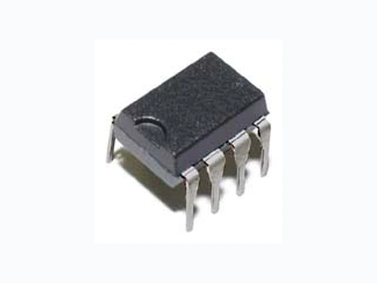
STR-A6252M ALLEGRO
Document overview
- Manufacturer or author: Provided By www.digicamel.com(free datasheet download site)
- PDF pages: 13
Technical content
All performance characteristics given are typical values for circuit or system baseline design only and are at the nominal operating voltage and .detats esiw re hto sselnu ,C°52+ fo erutarepmet tneibma na Universal-Input 20 W 67 kHz Flyback Switching Regulators STR-A6252M 67 kHz PWM with ±5% frequency jittering for EMI noise filtering and cost reduction Rugged 650 V avalanche-rated MOSFET:
- Simplified surge absorption
- No VDSS derating required Low RDS(on) : 2.8 Ω maximum Auto-burst mode for stand-by operation or light loads; less transformer audible noise Built-in leading edge blanking Soft start and low start-up current; start-up circuit disabled in operation Auto-burst stand-by (intermittent operation) input power <0.1 W at no load Built-in constant-voltage/constant current (CV/CC) Multiple protections:
- Pulse-by-pulse overcurrent protection (OCP)
- Overload protection (OLP) with auto restart
- Latching overvoltage protection (OVP)
- Undervoltage lockout (UVLO) with hysteresis
- Latching thermal shutdown (TSD) FEATURES AND BENEFITS STR-A6252M The STR-A6252M is a 67 kHz PWM topology (with ±5% frequency jittering for minimum EMI) regulator specifically designed to satisfy the requirements for increased integration and reliability in flyback converters. It incorporates a primary control and drive circuit with an avalanche-rated power MOSFET. This is a higher-frequency version of the STR-A6252. Covering the power range from below 24 watts for a
230 VAC input, or to 20 watts for a universal (85 to 264 VAC)
input, this device can be used in a wide range of applications, from DVD players and VCR player/recorders to ac adapters for cellular phones and digital cameras. An auto-burst standby function reduces power consumption at light load, while multiple protections, including the avalanche-energy guaranteed MOSFET, provide high reliability of system design. Cycle-by-cycle current limiting, undervoltage lockout with hysteresis, overvoltage protection, and thermal shutdown protect the power supply during the normal overload and fault conditions. Overvoltage protection and thermal shutdown are latched after a short delay. The latch may be reset by cycling the input supply. Low start-up current and a low-power standby mode selected from the secondary circuit completes a comprehensive suite of features. It is provided in an 8-pin mini-DIP plastic package with pin 6 removed. The leadframe plating is pure Sb, and the package complies with RoHS. Always order by complete part number, e.g.: Approximate Scale 1:1 Package DIP-8 SwitchingRegulators Datasheet 28103.44-5a www.datasheet4u.com
Universal-Input 20 W 67 kHz Flyback Switching Regulators Switching Regulators
115 Northeast Cutoff, Box 15036
Worcester, Massachusetts 01615-0036 FUNCTIONAL BLOCK DIAGRAM AND TERMINAL ASSIGNMENTS Drive
5 DVcc
2 LEB
3 GND
/OLP4 R SQ OCP CV/CC Istartup =1.1mA Frequency Modulation Soft Start UVLO RESET OLP 125°C OVP Feedback Control R S Q Delay 7.2V 10µs 13.4V/10V 7 D Number Name Description Functions
1 S/OCP Source/OCP terminal MOSFET Source/Overcurrent
2 FM/SS FM/Soft start terminal Capacitor connection terminal for
frequency jitter and soft start.
3 GND Ground terminal Ground
4 FB /CC/OLP FB/CC/OLP terminal
Input of constant voltage control signal / constant current operation control signal / over load protection signal
5 VCC Power supply terminal Input of power supply for control
D Drain terminals MOSFET drain / Input of startup current8 www.datasheet4u.com
Universal-Input 20 W 67 kHz Flyback Switching Regulators Switching Regulators Worcester, Massachusetts 01615-0036 ABSOLUTE MAXIMUM RATINGS at TA = 25°C Characteristic Symbol Terminal Note Max. Unit Drain Current1 IDpeak 8-1 Single Pulse 3.0 A Maximum Switching Current I DMAX 8-1 VS/OCP = 0.81 V with reference to GND, TA = –20 to 125°C 3.0 A Single Pulse Avalanche Energy2 EAS 8-1 Single Pulse 123 mJ VDD = 99 V, L = 20 mH, IL = 3.0 A 123 mJ S/OCP Terminal Voltage V OCP 1-3 –0.3 to 6 V Controller (MIC) Input Voltage Vcc 5-3 36 V FB/CC/OLP Terminal Voltage V FB 4-3 –0.3 to 12 V FM Terminal Voltage V FM 2-3 –0.3 to 6 V MOSFET Power Dissipation3,4 PD1 8-1 1.35 W Controller (MIC) Power Dissipation5 PD2 5-3 For Vcc×Icc 0.15 W Operating Internal Frame Temperature6 TF Refer to TOP –20 to 125 °C Operating Ambient Temperature T op –20 to 125 °C Storage Temperature T stg –40 to 125 °C Channel Junction Temperature T J 150 °C 1Refer to figure 1 2Refer to figure 3 3Refer to figure 5 4Mounted on 15 x 15 mm printed circuit board 5Refer to figure 6 6Measured at the root of terminal 3 Temperature, TF (°C) Safe Operating Area Temperature Derating Coefficient (%) 100 0 25 50 75 100 125 150 Drain-to-Source Voltage, VDS (V) Drain Current, ID (A)1.00 0.10 0.01 10.00 10 100 10001 1 ms 0.1 ms Current limit due to R DS(on) Refer to figure 1 for MOSFET SOA temperature derating coefficient Figure 1 – MOSFET Safe Operating Area Derating Curve Figure 2 – MOSFET Safe Operating Area Drain Current versus Voltage www.datasheet4u.com
Universal-Input 20 W 67 kHz Flyback Switching Regulators Switching Regulators Worcester, Massachusetts 01615-0036 Channel Junction Temperature, TJ (°C) EAS Derating Coefficient (%) 100 25 50 75 100 125 150 t( s ) Transient Thermal Resistance, RθJC (°C/W) 1.00 0.10 0.01 10.00 100µ10µ 10m 1m 100m1µ Ambient Temperature, TA (°C) Power Dissipation, PD1 (W) 0.2 0.4 0.6 0.8 1.0 1.2 1.4 1.6 0 20 40 60 80 100 120 140 160 PD1 = 1.35 W at TA & Internal Frame Temperature, TF (°C) Power Dissipation, PD2 (W) 0.2 0.4 0.6 0.8 1.0 1.2 1.4 1.6 0 20 40 60 80 100 120 140 160 PD2 = 0.15 W at TA & Figure 6 – MIC Power Dissipation versus Temperature Figure 3 – MOSFET Avalanche Energy Derating Curve Figure 4 – Transient Thermal Resistance Figure 5 – MOSFET Power Dissipation versus Temperature www.datasheet4u.com
Universal-Input 20 W 67 kHz Flyback Switching Regulators Switching Regulators Worcester, Massachusetts 01615-0036 ELECTRICAL CHARACTERISTICS for Controller (MIC), valid at TA = 25°C, VCC = 18 V, unless otherwise specified Characteristic Symbol Terminal Test Conditions Min. Typ. Max. Unit Operation Start Voltage V CC(ON) 5-3 (Power supply voltage at which device starts operating) Operation Stop Voltage V CC(OFF) 5-3 (Power supply voltage at which device stops operating) Measurement circuit 1, VCC = 15.7 through 9 to 11 V 91 0 1 1 V Circuit Current In Operation I CC(ON) 5-3 (Inflow current into power supply terminal, in operation) Measurement circuit 1 ––4 m A Initialization Circuit Current I CC(OFF) 5-3 (Inflow current into power supply terminal,, while subject to UVLO prior to operation) Measurement circuit 1, V CC = 12 V –– 2 5 μA Center Switching Frequency f osc(av) 8-3 (Center oscillation frequency of D terminal) Measurement circuit 2 60 67 74 KHz Frequency Jitter Deviation Δf 8-3 Maximum frequency – minimum frequency Measurement circuit 2 4.0 6.7 9.4 kHz Maximum Duty Cycle D MAX 8-3 (Maximum width of the low portion of the D terminal waveform) Measurement circuit 2 70 76 82 % FM High Voltage V HFM 2-3 (VFM at which the FM current is changed from 10 μA to –10 μA) Measurement circuit 2 4.0 4.5 5.0 V FM Low Voltage V LFM 2-3 (VFM at which the FM current is changed from –10 μA to 10 μA) Measurement circuit 2 3.2 3.6 4.0 V FM Outflow Current I sorcFM 2-3 Outflow current from FM terminal at VFM = VLFM (3.7 V typ.) Measurement circuit 2 7.7 11 15.4 μA FM Inflow Current I sinkFM 2-3 Inflow current into FM terminal at VFM = VHFM (4.4 V typ.) Measurement circuit 2 –15.4 –11 –7.7 μA OCP Threshold Voltage V OCP(th) 1-3 (The drain current at which the low portion of the D terminal waveform becomes shorter than the high portion, with V OCP increasing) Measurement circuit 3 0.67 0.74 0.81 V Leading Edge Blanking Time t wb 8-3 (The low portion of the D terminal waveform with VOCP = 1 V) Measurement circuit 3 240 350 460 ns Burst Threshold Voltage V burst(th) 4-3 (FB/CC/OLP terminal voltage at which D terminal waveform oscillation stops due to VFB decreasing from 5 V) Measurement circuit 4 1.0 1.12 1.24 V OLP Threshold Voltage V OLP(th) 4-3 (FB/CC/OLP terminal voltage at which D terminal waveform oscillation stops due to VFB increasing from 5 V) Measurement circuit 4 7.3 8.6 9.9 V Output Current at OLP Operation IOLP 4-3 (Outflow current from FB/CC/OLP terminal at VFB = 8 V) Measurement circuit 4 12 18 25 μA OLP Delay Time T OLP 4-3 (Time between surpassing VOLP(th) and stop of oscillation) Measurement circuit 4 0.84 1.2 1.56 s Maximum Feedback Current I FB(MAX) 4-3 (Outflow current from FB/CC/OLP terminal at VFB = 0 V) Measurement circuit 4 220 310 430 μA Continued on next page… www.datasheet4u.com
Universal-Input 20 W 67 kHz Flyback Switching Regulators Switching Regulators Worcester, Massachusetts 01615-0036 ELECTRICAL CHARACTERISTICS for Controller (MIC) continued, valid at TA = 25°C, VCC = 18 V, unless otherwise specified Constant Current Set Voltage V SET(CC) 4-3 (FB/CC/OLP terminal voltage at which IFB changes from 310 μA to 16 μA due to VFB increasing from 5 V) Measurement circuit 4 4.9 5.8 6.7 V Constant Current Reset Voltage VRES(CC) 4-3 (FB/CC/OLP terminal voltage at which IFB changes from 16 μA to 310 μA due to VFB decreasing from 8 V) VRES(CC) × VCC = 25 V, Measurement circuit 4, VCC = 25 V 3.5 3.9 4.3 V Start-Up Current I startup 6-3 (Outflow current from VCC terminal at VDD = 600 V) Measurement circuit 5, VCC = 13 V 0.77 1.1 1.43 mA OVP Threshold Voltage V CC(OVPth) 5-3 (VCC at which the oscillation of the D terminal waveform stops due to VCC increasing from 18 V) Measurement circuit 1, VCC = 18 through 31 to 35.2 V 28.8 32 35.2 V Latch Circuit Sustaining Current1 ICC(H) 5-3 (Inflow current into VCC at VCC = 8.4 V, after OVP operation) Measurement circuit 1, V CC = 35.2 to 8.6 V – – 270 μA Latch Circuit Release Voltage1 VCC(LaOFF) 5-3 (VCC at which ICC drops below 20 μA due to decreasing VCC after OVP operation) Measurement circuit 1, VCC = 35.2 through 5.9 to 8.6 V 5.9 7.2 8.6 V Thermal Shutdown Operating Temperature TJ(TSD) 125 140 – °C ELECTRICAL CHARACTERISTICS for MOSFET, valid at TA = 25°C, VCC = 18 V, unless otherwise specified Drain-to-Source Breakdown Voltage VDSS 8-1 Measurement circuit 6, I D = 300 μA 650 – – V Drain Leakage Current I DSS 8-1 (Inflow current into D terminal at VDD = 650 V) Measurement circuit 5 – – 300 μA On-Resistance R DS(ON) 8-1 Measurement circuit 3, I D = 0.4 A – – 2.8 Ω Switching Time t f 8-1 Measurement circuit 2 – – 250 ns Thermal Resistance R θch-F Between channel and internal frame; measured at the root of terminal 3 – – 52 °C/W 1Latch circuit enabled when OVP and TSD in operation www.datasheet4u.com
Universal-Input 20 W 67 kHz Flyback Switching Regulators Switching Regulators Worcester, Massachusetts 01615-0036 13V Vcc(ON ) Vcc(OF F) 18V Ic c (OFF) Vcc VD Ic c 18V Vcc(La.OFF)8.4V Ic c (H) Vcc VD Ic c Vcc(OVP ) Ic c 36V 150µA typ. 4µA typ. 1 2 3 4 8 7 5 S/OCP FM/SS FB/CC /OLP VCCDD STR-A6252M A 10V 1µF47nF Vcc +Ic cVDD VD 5.1V GND VD VFM VL FM VHFM VL FM+(VHFM-VL FM)/2 VCC 18V IFM fosc(av) IsinkFM fosc(H i) fosc(Lo)
- Dmax=T2/T1 100
- Δf =fosc(Hi)-fosc(Lo) IsorcFM0µA 1 2 3 4 8 7 5 S/OCP FM/SS FB/CC /OLP VCCDD STR-A6252M 10V 1µFVcc 100 Ω 100 Ω +VDD VD 5.1V GND A VFM IFM 18V 10V 90% 10% tf VD Vcc 18V VD VOCP Vocp VD(Lo) Tbw
- RDS(ON)=VD(Lo) /0 . 4 1 2 3 4 8 7 5 S/OCPFM/SS FB/CC /OLP VCCDD STR-A6252M 1µFVcc VD 5.1V GND 47nF VOCP 18V ID 0.4A Measurement Circuit 1 Measurement Circuit 2 Measurement Circuit 3 www.datasheet4u.com
Universal-Input 20 W 67 kHz Flyback Switching Regulators Switching Regulators Worcester, Massachusetts 01615-0036 Vcc Vburst VFB VD V(HYS) IFB(MAX) IFB VOLP IOLP VSET(CC) 18V VRST(CC) 18µA typ. 310µA typ.310µA typ. TOLP 25V 1 2 3 4 8 7 5 S/OCP FM/SS FB/CC /OLP VCCDD STR-A6252M 10V 1µF IFB +VDD GND VccA 47nF VFB 1 2 3 4 8 7 5 S/OCP FM/SS FB/CC /OLP VCCDD STR-A6252M 1µF VDD GND Vcc A ID A Ic c 1 2 3 4 8 7 5 S/OCP FM/SS FB/CC /OLP VCCDD STR-A6252M 1µF GND Vcc Ic c ID VD V 18V 300 µA L 1 2 3 4 8 7 5 S/OCP FM/SS FB/CC /OLP VCCDD STR-A6252M 1µF GND Vcc Ic c 18V VDS VGS VDD Vcc 18V VGS 8V VDS IL VDSpeak VDD T 100 Ω Measurement Circuit 4 Measurement Circuit 5 Measurement Circuit 6 Measurement Circuit 7 DDDS DS AS VpeakV peakVILpeakLE −= Adjust T such that ILpeak = 3.0 A www.datasheet4u.com
Universal-Input 20 W 67 kHz Flyback Switching Regulators Switching Regulators Worcester, Massachusetts 01615-0036 TYPICAL APPLICATION CIRCUIT For improved thermal dissipation, connect terminals 7 and 8 to as large an area of exposed copper as possible 8 7 5 1 2 3 4 VCCDD FB/CC /OLPFM/SS STR-A6252 S/OCP 85~ 265VAC GND OUT GND PC PC Function of External Parts Mode R4 R5 CV/CC 1 to 1.8 M Ω 82 to 150 kΩ OLP None None www.datasheet4u.com
Universal-Input 20 W 67 kHz Flyback Switching Regulators Switching Regulators Worcester, Massachusetts 01615-0036 Dimens ions in Inches (for reference only) Dimens ions in Millimeters (controlling dime ns ions ) PACKAGE DIMENSIONS, DIP-8 www.datasheet4u.com
Universal-Input 20 W 67 kHz Flyback Switching Regulators Switching Regulators Worcester, Massachusetts 01615-0036 PACKING SPECIFICATIONS 510 130 140 524 145 265 520 290 135 535 Type A Type B 50 pieces Stopper, with attached tabOrientation of Devices in Shipping Tubes Stopper, with no tab Minimum packing option: Tubes Shipping Tube Dimensions Inner Carton Dimensions Capacity: 50 tubes per inner carton Outer Carton Dimensions Capacity: 4 inner cartons per outer carton; 10,000 devices maximum per outer carton All dimensions: mm www.datasheet4u.com
Universal-Input 20 W 67 kHz Flyback Switching Regulators Switching Regulators Worcester, Massachusetts 01615-0036 Because reliability can be affected adversely by improper storage environments and handling methods, please observe the following cautions. Cautions for Storage
- Ensure that storage conditions comply with the standard temperature (5°C to 35°C) and the standard relative humidity (around 40 to 75%); avoid storage locations that experience extreme changes in temperature or humidity.
- Avoid locations where dust or harmful gases are present and avoid direct sunlight.
- Reinspect for rust in leads and solderability of products that have been stored for a long time. Cautions for Testing and Handling When tests are carried out during inspection testing and other standard test periods, protect the products from power surges f rom the testing device, shorts between adjacent products, and shorts to the heatsink. Remarks About Using Silicone Grease with a Heatsink
- When silicone grease is used in mounting this product on a heatsink, it shall be applied evenly and thinly. If more silicone grease than required is applied, it may produce stress.
- Volatile-type silicone greases may produce cracks after long periods of time, resulting in reduced heat radiation effect. Silicone grease with low consistency (hard grease) may cause cracks in the mold resin when screwing the product to a heatsink.
- Our recommended silicone greases for heat radiation purposes, which will not cause any adverse effect on the product life, are indicated below: Type Suppliers G746 Shin-Etsu Chemical Co., Ltd. YG6260 Toshiba Silicone Co., Ltd. SC102 Dow Corning Toray Silicone Co., Ltd. Soldering
- When soldering the products, please be sure to minimize the working time, within the following limits: 260±5°C 10 s 350±5°C 3 s
- Soldering iron should be at a distance of at least 1.5 mm from the body of the products Electrostatic Discharge
- When handling the products, operator must be grounded. Grounded wrist straps worn should have at least 1 M Ω of resistance to ground to prevent shock hazard.
- Workbenches where the products are handled should be grounded and be provided with conductive table and floor mats.
- When using measuring equipment such as a curve tracer, the equipment should be grounded.
- When soldering the products, the head of soldering irons or the solder bath must be grounded in other to prevent leak voltage s generated by them from being applied to the products.
- The products should always be stored and transported in our shipping containers or conductive containers, or be wrapped in al uminum foil. WARNING — These devices are designed to be operated at lethal voltages and energy levels. Circuit designs that embody these components must conform with applicable safety requirements. Pre cau tions must be taken to prevent accidental contact with power-line potentials. Do not connect ground ed test equipment. The use of an isolation transformer is recommended during circuit development and breadboarding. www.datasheet4u.com
Universal-Input 20 W 67 kHz Flyback Switching Regulators Switching Regulators Worcester, Massachusetts 01615-0036 The products described herein are manufactured in Ja pan by Sanken Electric Co., Ltd. for sale by Allegro MicroSystems, Inc. Sanken and Allegro reserve the right to make, from time to time, such de par tures from the detail spec i fi ca tions as may be re quired to per mit im- prove ments in the per for mance, reliability, or manufacturability of its prod ucts. Therefore, the user is cau tioned to verify that the in for ma tion in this publication is current before placing any order. When using the products described herein, the ap pli ca bil i ty and suit abil i ty of such products for the intended purpose shall be reviewed at the users responsibility. Although Sanken undertakes to enhance the quality and reliability of its prod ucts, the occurrence of failure and defect of semi con duc tor products at a certain rate is in ev i ta ble. Users of Sanken products are requested to take, at their own risk, preventative measures including safety design of the equipment or systems against any possible injury, death, fires or damages to society due to device failure or malfunction. Sanken products listed in this publication are designed and intended for use as components in general-purpose electronic equip ment or apparatus (home ap pli anc es, office equipment, tele com mu ni ca tion equipment, measuring equipment, etc.). Their use in any application requiring radiation hardness assurance (e.g., aero space equipment) is not supported. When considering the use of Sanken products in ap pli ca tions where higher reliability is re quired (transportation equipment and its control systems or equip ment, fire- or burglar-alarm systems, various safety devices, etc.), contact a company sales representative to discuss and obtain written confirmation of your spec i fi ca tions. The use of Sanken products without the written consent of Sanken in applications where ex treme ly high reliability is required (aerospace equip- ment, nuclear power-control stations, life-support systems, etc.) is strictly prohibited. The information in clud ed herein is believed to be accurate and reliable. Ap pli ca tion and operation examples described in this pub li ca tion are given for reference only and Sanken and Allegro assume no re spon si bil i ty for any in fringe ment of in dus tri al property rights, intellectual property rights, or any other rights of Sanken or Allegro or any third party that may result from its use. Copyright © 2006 Allegro MicroSystems, Inc. This datasheet is based on Sanken datasheet SSE-23421 www.datasheet4u.com